 | –≠–ª–µ–∫—Ç—Ä–æ–Ω–Ω—ã–π –∫–æ–º–ø–æ–Ω–µ–Ω—Ç: MIC2550 | –°–∫–∞—á–∞—Ç—å:  PDF PDF  ZIP ZIP |

October 4, 1999
1
MIC2550
MIC2550
Micrel
MIC2550
Universal Serial Bus Transceiver
Advance Information
General Description
The MIC2550 is a single-chip transceiver that complies with
the physical layer specifications for Universal Serial Bus
(USB).
The MIC2550 supports full-speed (12Mb/s) dual supply volt-
age operation (patent pending) and low-speed (1.5Mb/s)
operation.
A unique dual supply voltage operation allows the MIC2550
to reference the system I/F I/O signals to a supply voltage
down to 2.5V while independently powered by the USB V
BUS
.
This allows the system interface to operate at its core voltage
without addition of buffering logic and also reduce system
operating current.
System Diagram
Features
∑ Compliant to
USB Specification Revision 1.1
∑ Operation down to 2.5V
∑ Dual supply voltage operation
∑ Supports full-speed (12Mb/s) and
low-speed (1.5Mb/s) operation
∑ Speed-select termination supply
∑ Very low power consumption meets
USB suspend-current requirements
∑ Small 14-pin TSSOP
Applications
∑ Personal digital assistants (PDA)
∑ Palmtop computers
∑ Cellular telephones
Ordering Information
Part Number
Junction Temp. Range
Package
MIC2550BTS
≠40
∞
C to +85
∞
C
14-Pin TSSOP
System
Supply
Voltage
System
Interface
VIF
SPD
OE#
RCV
VP
VM
D≠
D+
VBUS
VTRM
GND
D≠
D+
V
BUS
USB
Interface
Connector
GND
24
24
1.5k
GND
HIGH
SPEED
LOW
SPEED
MIC2550
SUS
1µF
0.47µF
Micrel, Inc. ∑ 1849 Fortune Drive ∑ San Jose, CA 95131 ∑ USA ∑ tel + 1 (408) 944-0800 ∑ fax + 1 (408) 944-0970 ∑ http://www.micrel.com
MIC2550
Micrel
MIC2550
2
October 4, 1999
Pin Description
Pin Number
Pin Name
Pin Function
1
VIF
System Interface Supply Voltage (Input): Determines logic voltage levels for
system interface signaling to logic controller.
2
SPD
Speed (Input): Edge rate control. Logic high selects full-speed edge rates.
Logic low selects low-speed edge rates.
3
RCV
Receive Data (Output): System interface receive data interface to logic
controller.
4
VP
Plus (Input/Output): System interface signal to logic controller. If OE# is
logic 1, VP is a receiver output (+); If OE# is logic 0, VP is a driver input (+).
5
VM
Minus (Input/Output): System interface signal to logic controller. If OE# is
logic 1, VM is a receiver output (≠); If OE# is logic 0, VM is a driver input (≠).
6, 13
NC
not internally connected
7
GND
Ground: Power supply return and signal reference.
8
SUS
Suspend (Input): Logic high turns off internal circuits to reduce supply
current.
9
OE#
Output Enable (Input): Active-low system interface input signal from from
logic controller. Logic low causes transceiver to transmit data onto the bus.
Logic high causes the transceiver to receive data from the bus.
10
D≠
USB Differential Data Line ≠ (Input/Output)
11
D+
USB Differential Data Line + (Input/Output)
12
VTRM
Termination Supply (Output): 3.3V speed termination resistor supply output.
14
VBUS
USB Supply Voltage (Input): Transceiver supply.
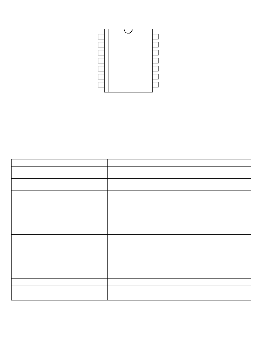
Pin Configuration
2
SPD
3
RCV
4
VP
5
VM
6
NC
7
GND
1
VIF
VBUS
14
NC
13
VTRM
12
D+
11
D≠
10
OE#
9
8
SUS
14-Pin TSSOP (TM)

October 4, 1999
3
MIC2550
MIC2550
Micrel
Absolute Maximum Ratings
(Note 1)
Supply Voltage (V
IF
) ................................................... +6.5V
Input Voltage (V
BUS
) ........................ ≠0.5V(min)/5.5V(max)
Output Current (I
D+
, I
D≠
) ...........................................
±
50mA
Output Current (all others) .......................................
±
15mA
Input Current ............................................................
±
50mA
Power Dissipation (P
D
) ................................................ TBD
Storage Temperature (T
S
) .......................... ≠65
∞
to +150
∞
C
ESD, Note 3
Operating Ratings
(Note 2)
Supply Voltage (V
BUS
) ................................. 4.0V to 5.25V
Temperature Range (T
A
) ........................... ≠40
∞
C to +85
∞
C
Junction Temperature (T
J
) ........................................ 160
∞
C
Package Thermal Resistance
TSSOP
(
JA
) ..................................................... 100
∞
C/W
Electrical Characteristics
T
A
= 25
∞
C, bold values indicate ≠40
∞
C
T
A
+85
∞
C; typical values at V
BUS
= 5.0V, V
IF
= 3.0V; minimum and maximum values at
V
BUS
= 4.0V to 5.25V, V
IF
= 2.5V to 3.6V; unless noted.
Symbol
Parameter
Condition
Min
Typ
Max
Units
System and USB Interface DC Characteristics
V
BUS
USB Supply Voltage
4.0
5.25
V
V
IF
System I/F Supply voltage
2.5
5.25
V
V
IL
Low-Level Input Voltage, Note 4
0.15V
IF
V
V
IH
High-Level Input Voltage, Note 4
0.85V
IF
V
V
OH
High-Level Output Voltage, Note 4
I
OH
= 20
µ
A
0.9V
IF
V
V
OL
Low-Level Output Voltage, Note 4
I
OL
= 20
µ
A
0.1
V
I
IL
Input Leakage Current, Note 4
±
5
µ
A
I
IF
System I/F Supply Current
D≠ and D+ are idle, V
IF
= 3.6V, V
BUS
= 5.25V
1
µ
A
SUS = 1, OE# = 1
D≠ and D+ are idle, V
IF
= 3.6V, V
BUS
= 5.25V
1
µ
A
SUS = 0, OE# = 1
D≠ and D+ active, C
LOAD
= 50pF, SPD = 1,
2
µ
A
SUS = 0, V
IF
= 3.6V, OE# = 0
D≠ and D+ active, C
LOAD
= 600pF, SPD = 0,
2
µ
A
SUS = 0, V
IF
= 3.6V, OE# = 0
I
BUS
USB Supply Current
D≠ and D+ are idle, V
BUS
= 5.25V, SPD = 0
140
200
µ
A
SUS = 1, OE# = 1
D≠ and D+ are idle, V
BUS
= 5.25V, SPD = 1
140
200
µ
A
SUS = 1, OE# = 1
D≠ and D+ are idle, V
BUS
= 5.25V, SPD = 0
140
200
µ
A
SUS = 0, OE# = 0
D≠ and D+ are idle, V
BUS
= 5.25V, SPD = 1
200
350
µ
A
SUS = 0, OE# = 1
D≠ and D+ active, C
LOAD
= 50pF, SPD = 1,
mA
SUS = 0, V
BUS
= 5.25V
D≠ and D+ active, C
LOAD
= 600pF, SPD = 0
mA
SUS = 0, V
BUS
= 5.25V
V
TRM
Termination Voltage
I
TRM
= 2.5mA
3.0
3.6
V
MIC2550
Micrel
MIC2550
4
October 4, 1999
Symbol
Parameter
Condition
Min
Typ
Max
Units
Transceiver DC Characteristics
I
LO
Hi-Z State Data Line Leakage
0V < V
BUS
< 3.3V, D+, D≠, OE# = 1 pins only
≠10
+10
µ
A
V
DI
Differential Input Sensitivity
(D+) ≠ (D≠)
, V
IN
= 0.8V ≠ 2.5V
0.2
V
V
CM
Differential Common-Mode Range
includes V
DI
range
0.8
2.5
V
V
SE
Single-Ended Receiver Threshold
0.8
2.0
V
Receiver Hysteresis, Note 6
200
mV
V
OL
Static Output Low, Note 5
OE# = 0, R
L
= 1.5k
to 3.6V
0.3
V
V
OH
Static Output High, Note 5
OE# = 0, R
L
= 15k
to GND
2.8
3.6
V
V
CRS
Output Signal Crossover Voltage
1.3
2.0
V
Note 6
C
IN
Transceiver Capacitance, Note 6
pin to GND
20
pF
Z
DRV
Driver Output Resistance
steady state drive, Note 6
6
18
Low-Speed Driver Characteristics
t
R
Transition Rise Time
C
L
= 50pF
75
ns
C
L
= 600pF
300
ns
t
F
Transition Fall Time
C
L
= 50pF
75
ns
C
L
= 600pF
300
ns
t
R
/t
F
Rise and Fall Time Matching
T
R
˜
T
F
80
125
%
V
CRS
Output Signal Crossover Voltage
1.3
2.0
V
Full-Speed Driver Characteristics
t
R
Transition Rise Time
C
L
= 50pF
4
20
ns
t
F
Transition Fall Time
C
L
= 50pF
4
20
ns
t
R
/t
F
Rise and Fall Time Matching
T
R
˜
T
F
90
111.11
%
V
CRS
Output Signal Crossover Voltage
1.3
2.0
V
Note 1.
Exceeding the absolute maximum rating may damage the device.
Note 2.
The device is not guaranteed to function outside its operating rating.
Note 3.
Devices are ESD sensitive. Handling precautions recommended.
Note 4.
Applies to the VP, VM, RCV, OE#, SPD, and SUS pins.
Note 5.
Applies to D+, D≠
Note 6.
Not production tested. Guaranteed by design.
October 4, 1999
5
MIC2550
MIC2550
Micrel
Symbol
Parameter
Condition
Min
Typ
Max
Units
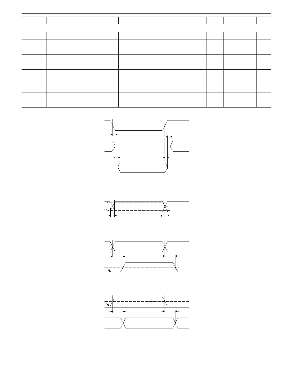
Transceiver Timing
t
PVZ
OE# to RCVR Tristate Delay
Figure 1
15
ns
t
PZD
Receiver Tristate to Transmit Delay
Figure 1
15
ns
t
PDZ
OE# to DRVR Tristate Delay
Figure 1
15
ns
t
PZV
Driver Tri-state to Receiver Delay
Figure 1
15
ns
t
PLH
V+/V≠ to D+/D≠ Propagation Delay
Figure 4
15
ns
t
PHL
V+/V≠ to D+/D≠ Propagation Delay
Figure 4
15
ns
t
PLH
D+/D≠ to RCV Propagation Delay
Figure 3
15
ns
t
PHL
D+/D≠ to RCV Propagation Delay
Figure 3
15
ns
t
PLH
D+/D≠ to V+/D≠ Propagation Delay
Figure 3
8
ns
t
PHL
D+/D≠ to V+/D≠ Propagation Delay
Figure 3
8
ns
V
M
V
P
V
P
/V
M
t
PVZ
t
PZV
V
OE#
H
L
t
PZD
V
D+
/V
D≠
V
D≠
V
D+
Figure 1. Enable and Disable Times
10%
V
D≠
V
D+
Differential
Data
Lines
90%
t
R
t
F
V
CRS
Figure 2. Rise and Fall Times
V
D≠
V
D+
Differential
Data
Lines
t
PLH
t
PHL
Output
V
OH
V
OL
V
SS
Figure 3. Receiver Propagaion Delay D+/D≠ to RCV, V
P
, and V
M
V
D≠
V
D+
Differential
Data
Lines
t
PLH
t
PHL
Input
V
OI
V
OL
V
SS
Figure 4. Driver Propagation Delay V
P
and V
M
to D+/D≠
MIC2550
Micrel
MIC2550
6
October 4, 1999
:
)
t
i
m
s
n
a
r
T
(
0
=
#
E
O
t
u
p
n
I
t
u
p
t
u
O
t
l
u
s
e
R
P
V
M
V
+
D
≠
D
V
C
R
0
0
0
0
X
0
E
S
0
1
0
1
0
0
c
i
g
o
L
1
0
1
0
1
1
c
i
g
o
L
1
1
1
1
X
d
e
n
i
f
e
d
n
U
:
)
e
v
i
e
c
e
R
(
1
=
#
E
O
t
u
p
n
I
t
u
p
t
u
O
t
l
u
s
e
R
+
D
≠
D
P
V
M
V
V
C
R
0
0
0
0
X
0
E
S
0
1
0
1
0
0
c
i
g
o
L
1
0
1
0
1
1
c
i
g
o
L
1
1
1
1
X
d
e
n
i
f
e
d
n
U
Table 1. Truth Table
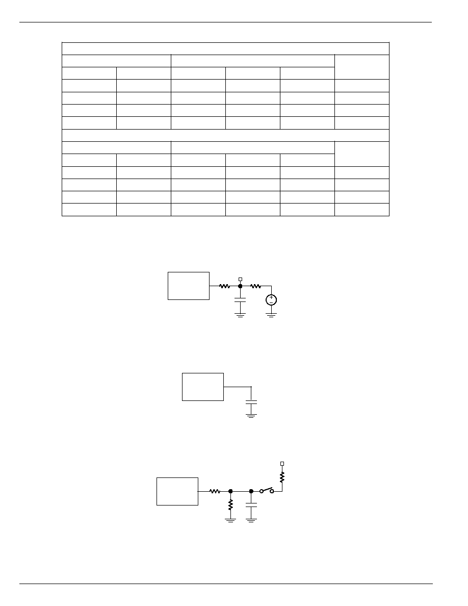
Test Circuits
Device
Under
Test
50pF
24
For D+/D≠:
V = 0V for t
PZH
and t
PHZ
V = V
BUS
for t
PZL
and t
PLZ
V
Test
Point
500
Load for Enable and Disable Time (D+/D≠)
Device
Under
Test
25pF
V
P
, V
M
, and RCV Load
Device
Under
Test
15k
C
L
V
TRM
1.5k
*
24
C
L
= 50pF, full speed
C
L
= 50pF, low speed (minimum timing)
C
L
= 600pF, low speed (maximum timing)
*1.5k on D≠ for low speed or D+ for high speed
D+ and D≠ Load

October 4, 1999
7
MIC2550
MIC2550
Micrel
Block Diagram
Regulator
VM
GND
VP
RCV
OE#
SPD
VIF
D≠
D+
VBUS
VTRM
USB VOLTAGE DOMAIN
SYSTEM I/F
VOLTAGE DOMAIN
TO
INTERNAL
CIRCUITS
SUS
Applications Information
The MIC2550 is designed to provide USB connectivity in
mobile systems where system supply voltages are not avail-
able to satisfy USB requirements. The MIC2550 can operate
down to supply voltages of 2.5V and still meet USB physical
layer specifications. As shown in the system diagram, the
MIC2550 takes advantage of USB's supply voltage, V
BUS
, to
operate the transceiver. The system voltage, V
IF
, is used to
set the reference voltage used by the digital I/O lines (VP, VM,
RCV, OE#, SPD, and SUS pins) interfacing to the system.
Internal circuitry provides translation between the USB and
system voltage domains. V
IF
will typically be the main supply
voltage rail for the system.
In addition, a 3.3V, 10% termination supply voltage, V
TRM
, is
provided to support speed selection. A 0.47
µ
F (minimum)
capacitor from V
TRM
to ground is required to ensure stability.
A 1.5K resistor is required between this pin and the D+ or D≠
lines to respectively specify full-speed or low-speed opera-
tion.
Suspend
When the suspend pin (SUS) is high, power consumption is
reduced to a minimum. V
TRM
is not disabled. RCV, VP and
VM are still functional to enable the device to detect USB
activity. For minimal current consumption in suspend mode,
it is recommended that OE# = 1.
External ESD Protection
The use of ESD transient protection devices is not required
for operation, but is recommended.
Nonmultiplexed Bus
To save pin count for the USB logic controller interface, the
MIC2550 was designed with V
P
and V
M
as bidirectional pins.
To interface the MIC2550 with a nonmultiplexed data bus,
resistors can be used for low cost isolation as shown in
Figure 6.
V
PO
V
P
V
M
V
MO
USB Logic
Controller
(SIE)
MIC2550
V
P
V
M
10k
10k
Figure 6. MIC2550 Interface to
Nonmultiplexed Data Bus.

MIC2550
Micrel
MIC2550
8
October 4, 1999
Package Information
1.10 MAX (0.043)
0.15 (0.006)
0.05 (0.002)
1.00 (0.039) REF
0.65 BSC
(0.026)
8
∞
0
∞
6.4 BSC (0.252)
5.10 (0.200)
4.90 (0.193)
0.20 (0.008)
0.09 (0.003)
0.70 (0.028)
0.50 (0.020)
DIMENSIONS:
MM (INCH)
4.50 (0.177)
4.30 (0.169)
0.30 (0.012)
0.19 (0.007)
14-Pin TSSOP (TS)
MICREL INC.
1849 FORTUNE DRIVE
SAN JOSE, CA 95131
USA
TEL
+ 1 (408) 944-0800
FAX
+ 1 (408) 944-0970
WEB
http://www.micrel.com
This information is believed to be accurate and reliable, however no responsibility is assumed by Micrel for its use nor for any infringement of patents or
other rights of third parties resulting from its use. No license is granted by implication or otherwise under any patent or patent right of Micrel Inc.
© 1999 Micrel Incorporated