February 2005
1
MIC2580A
MIC2580A
Micrel, Inc.
MIC2580A
Hot-Swap PCI Power Controller
General Description
The MIC2580A is a hot-swap controller that provides for safe
and orderly insertion and removal of PCI based adapter cards
from a PCI hot-plug compliant system backplane or
CompactPCITM system.
The MIC2580A incorporates a circuit breaker function that
protects all four supplies (+12V, +5V, +3.3V, and ≠12V) upon
an overcurrent fault condition. Current foldback limiting pre-
vents large transient currents caused by plugging adapter
cards into live backplanes, such as in a CompactPCI system.
A programmable slew-rate control limits high inrush currents
to all loads that occur when power is applied to large capaci-
tive loads.
Voltage supervisory functions for all four power supplies are
provided by "power good" (/PWRGD) and "overcurrent fault"
(/FAULT) diagnostic outputs. Power good and overcurrent
fault include deglitch filters to prevent nuisance tripping.
Power good is active when all four supplies are within
tolerance. Fault (/FAULT) goes active upon overcurrent or
overtemperature conditions. The on-off control input (/ON) is
used to cycle power to the adapter card.
Typical Application
12VOUT
5VGATE
3VGATE
VPCHG
12VIN
/FAULT
GND
CSTART
/LPCIRST
5VIN
3VIN
/PCIRST
/EPWRGD
/ON
CSLEW
MIC2580A
5VSENSE
3VSENSE
5VOUT
3VOUT
/POR
CRST
IRF7413
IRF7413
+3.3V
+5V
+12V
/PWRGD
M12VIN
M12VOUT
+12V
+5V
+3.3V
GND
≠12V
≠12V
10m
10m
V
PCH
= +1V ±20%
(PRECHARGE SUPPLY)
Data Bus
/HEALTHY
/BD_SEL
/PCI_RST
VIO
≠12V/1A
GND
+3.3V/8A
+5V/8A
+12V/1A
/ENUM
Data Bus
/ON
/PCIRST
/PGD
Adapter
Platf
or
m
Overcurrent
Fault
V
IO
D0
D0
D1
D1
D2
D2
Dn
Dn
V
IO
PCI
Controller
/LPCIRST
1.2k
1µF
1µF
1µF
1µF
CompactPCITM Adapter with Early Power
Features
∑ PCI hot-plug and CompactPCITM hot-swap support
∑ +12V, +5V, +3.3V, and ≠12V power supply control
∑ Circuit breaker function to protect system
∑ Programmable slew rate control for all supplies
∑ Foldback current-limiting
∑ +5V and +3.3V programmable current-limit thresholds
∑ Undervoltage and overcurrent diagnostic outputs
∑ Deglitch filters on diagnostic fault outputs
∑ Integrated +12V and ≠12V MOSFET switches
∑ Integrated high-side drivers for 3.3V and 5V external
switches
∑ Precharge supply for CompatPCITM I/O termination
Applications
∑ PCI hot-plug systems
∑ CompactPCITM hot-swap systems
Micrel, Inc. ∑ 2180 Fortune Drive ∑ San Jose, CA 95131 ∑ USA ∑ tel + 1 (408) 944-0800 ∑ fax + 1 (408) 474-1000 ∑ http://www.micrel.com
CompactPCI is a trademark of the PCI Industrial Computer Manufacturer's Group.
MIC2580A
Micrel, Inc.
MIC2580A
2
February 2005
Pin Configuration
1
12VOUT
3VGATE
3VOUT
3VSENSE
3VIN
/PCIRST
/LPCIRST
/EPWRGD
/PWRGD
VPCHG
24 12VIN
5VGATE
5VOUT
5VSENSE
5VIN
/FAULT
CSTART
CSLEW
/POR
CRST
23
22
21
20
19
18
17
16
15
2
3
4
5
6
7
8
9
10
GND
/ON
11
M12VIN
M12VOUT
12
14
13
24-lead TSSOP (TS)
Pin Description
Pin Number
Pin Name
Pin Function
1
12VOUT
+12V Switched Supply (Output): Load carrying output.
2
3VGATE
3.3V Gate Drive (Output): Drives gate of external N-channel MOSFET +3V
switch. Adding capacitance will slow the slew rate of the external MOSFET
switch turn-on. (The external MOSFET's gate is charged by an internal
current source.)
3
3VOUT
+3.3V Output Voltage Sense (Input): Connect to source of external
N-channel MOSFET (+3V switched output) to monitor for output undervolt-
age conditions.
4
3VSENSE
+3.3V Current Sense (Input): Measures voltage drop across an external
sense resistor with respect to 3VIN for overcurrent detection through the
+3.3V switch.
5
3VIN
3V Supply (Input): +3.3V-supply input for current monitoring (reference input
for 3VSENSE). Not a load-current carrying input.
6
/PCIRST
PCI-Bus Reset (Input): Input from PCI bus that resets the internal logic.
Ordering Information
Part Number
Precharge
Temperature
Standard
Pb-Free
Voltage
Range
Package
MIC2580A-1.0BTS
MIC2580A-1.0YTS
1V
≠40∞C to +85∞C
24-lead TSSOP
MIC2580A-1.6BTS
MIC2580A-1.6YTS
1.6V
≠40∞C to +85∞C
24-lead TSSOP

February 2005
3
MIC2580A
MIC2580A
Micrel, Inc.
Pin Number
Pin Name
Pin Function
7
/LPCIRST
Local PCI Reset (Open-Drain Output): Local PCI reset output to PCI
controller. Compliant to CompactPCI specification for LOCAL_PCI_RESET.
8
/EPWRGD
Early Power Good (Open-Drain Output): This signal goes active should
/FAULT or /PWRGD go active. No deglitch filtering is provided. This signal
satisfies PCI /RST timing for T
FAIL
per PCI Local Bus Specification, ver-
sion 2.1.
9
/PWRGD
Power Good (Open-Drain Output): Active-low output goes active when all
supplies are within tolerance. (A 20µs delay is inserted prior to activation to
reduce nuisance tripping.)
10
VPCHG
Precharge Supply (Output): (MIC2580A-1.0) +1V ±20% supply used for
precharge bias for I/O terminations (CompactPCI only).
11
GND
Ground
12
M12VIN
≠12V Supply (Input): Input for internal ≠12V switch.
13
M12VOUT
≠12V Switched Supply (Output): Switched ≠12V supply to PCI Hot Plug
compliant socket. Load carrying output.
14
/ON
On-Off Control (Input): Logic low turns on all switches; logic high turns off all
switches. Also used to reset the device from a circuit breaker condition. The
/ON pin is edge-triggered and requires a high-to-low transition once all four
supplies are above their respective thresholds.
15
CRST
Reset Delay (External Component): Connect to external capactior (C
RST
) to
increase power-on reset delay.
16
/POR
Reset (Open-Drain Output): Active-low signal remains active for a time
determined by C
RST
after all supplies are within tolerance; i.e., /PWRGD is
active. This signal may be used as a reset for logic controllers.
17
CSLEW
Slew (External Component): Connect to external capacitor (C
SLEW
) to
program the output slew rate of 3VGATE, 5VGATE, 12VGATE (internal) and
M12VGATE (internal).
18
CSTART
Start-Up Timer (External Component): Connect to external capacitor
(C
START
) to increase the filter delay used to gate the /FAULT output upon
start-up. Used to prevent nuisance tripping during turn-on of supplies.
19
/FAULT
Fault (Open-Drain Output/Input): This active-low output signal activated
upon overcurrent or thermal shutdown. Includes 20µs deglitch filter. Fault is
reset using /ON.
Forcing pin low turns off all switches but does not activate the circuit breaker
function.
20
5VIN
5V Supply (Input): +5V-supply input for current monitoring (reference
voltage for 5VSENSE). Not a load-current carrying input.
21
5VSENSE
+5V Current Sense (Input): Measures voltage drop across an external
sense resistor with respect to 5VIN for overcurrent detection through the +5V
switch.
22
5VOUT
+5V Output Voltage Sense (Input): Connect to source of external N-channel
MOSFET (+5V switched output) to monitor for output undervoltage condi-
tions.
23
5VGATE
5V Gate Drive (Output): Drives gate of external N-channel MOSFET +5V
switch. Adding capacitance will slow the slew rate of the external MOSFET
switch turn-on. (The external MOSFET's gate is charged by an internal
current source.)
24
12VIN
12V Supply (Input): MIC2580A power supply and input for internal +12
switch. Supplies power for internal circuitry.

MIC2580A
Micrel, Inc.
MIC2580A
4
February 2005
Absolute Maximum Ratings
(Note 1)
Supply Voltages
+12V Input (V
12VIN
) ................................................. +14V
+5V Input (V
5VIN
) ....................................................... +7V
+3.3V Input (V
3VIN
) .................................................... +7V
≠12V Input (V
M12VIN
) ............................................... ≠14V
/PWRGD, /FAULT, /POR, /EPWRGD, and /PCIRST
Output Current ........................................................... 10mA
Lead Temperature (Soldering)
Standard Package (-x.xBTS)
IR Reflow ......................................... 240∞C + 0∫C/-5∫C
Lead-free Package (-x.xYTS)
IR Reflow ......................................... 260∫C + 0∫C/-5∫C
ESD Rating, Note 3
Human body model ................................................... 2kV
Operating Ratings
(Note 2)
Supply Voltages
+12V Input (V
12VIN
) ............................. +11.4V to +12.6V
≠12V Input (V
M12VIN
) ........................... ≠11.4V to ≠12.6V
+5V Input (V
5VIN
) ................................... +4.75V to +5.25
+3.3V Input (V
3VIN
) .............................. +3.125V to +3.5V
Temperature Range (T
A
) ........................... ≠40∞C to +85∞C
Junction Temperature (T
J
) ........................................ 150∞C
Package Thermal Resistance (
JA
)
24-Lead TSSOP .................................................. 83∞C/W
Electrical Characteristics
V
12VIN
= 12V, V
5VIN
= 5V, V
3VIN
= 3.3V, V
M12VIN
= ≠12V; T
A
= 25∞C, bold values indicate ≠40∞C T
A
+85∞C; unless noted
Symbol
Parameter
Condition
Min
Typ
Max
Units
I
12IN
Supply Current
/ON > V
IH
2.2
3
mA
I
5IN
4
6
mA
I
3IN
0.23
0.4
mA
I
12MIN
3
5
mA
V
UVLO
Undervoltage Lockout
V
12VIN
increasing
8.9
9.8
V
V
12VIN
UVLO hysteresis
300
mV
V
M12VIN
decreasing
-10.5
-8.3
V
V
M12VIN
UVLO hysteresis
100
mV
V
5VIN
increasing
2.1
3.1
V
V
5VIN
UVLO hysteresis
20
mV
V
3VIN
increasing
2.4
2.6
V
V
3VIN
UVLO hysteresis
60
mV
V
5VGATE
5VGATE Voltage
10.5
11
V
V
3VGATE
3VGATE Voltage
10.5
11
V
I
5VGATE
5VGATE Output Current
during start-up, V
5VGATE
= 5V
≠40
µA
during turnoff; /FAULT = 0
6
mA
I
3VGATE
3VGATE Output Current
during start-up, V
5VGATE
= 5V
≠40
µA
during turnoff; /FAULT = 0
6
mA
V
PGTH
Power Good Threshold Voltage
V
12VOUT
increasing
11
11.4
V
V
12VOUT
Power-Good hysteresis
200
mV
V
M12VOUT
decreasing
≠11.2
≠10
V
V
M12VOUT
Power-Good hysteresis
50
mV
V
5VOUT
increasing
4.45
4.7
V
V
5VOUT
Power-Good hysteresis
100
mV
V
3VOUT
increasing
2.90
3.10
V
V
3VOUT
Power-Good hysteresis
60
mV
V
IL
Input Voltage Level (/ON)
logic low
0.8
V
V
IH
logic high
2.0
V
I
IL
Input Leakage Currnet (/ON)
≠1
1
µA

February 2005
5
MIC2580A
MIC2580A
Micrel, Inc.
Symbol
Parameter
Condition
Min
Typ
Max
Units
V
OL
Output-Low Voltage
I
OL
= 2mA
0.4
V
(/PWRGD, /FAULT, /POR,
EPWRGD, /LPCIRST)
T
OV
Overtemperature Shutdown
T
J
increasing
170
∞C
Threshold
T
J
decreasing
160
∞C
I
CRST
CRST Charge Current
during turn-on
≠9
≠11.5
µA
I
CSTART
CSTART Charge Current
during turn-on
≠9
≠11.5
µA
I
CSLEW
CSLEW Charge Current
during turn-on
≠30
≠39
≠45
µA
R
DS(on)12
Output MOSFET Resistance
+12V internal MOSFET, I
DS
= 500mA
450
600
m
R
DS(on)M12
≠12V internal MOSFET, I
DS
= 200mA
430
600
m
Output MOSFET Leakage
+12V internal MOSFET
≠100
100
µA
≠12V internal MOSFET
0
300
µA
V
CLTH
Current Limit Threshold Voltage
V
5VIN
≠ V
5VSENSE
45
56
67
mV
V
3VIN
≠ V
3VSENSE
45
55
67
mV
I
LIM12
Current-Limit
+12V internal MOSFET, ramped load
1.0
1.3
1.5
A
I
LIM12M
Threshold
≠12V internal MOSFET, ramped load
≠0.4
≠0.5
≠0.7
A
Short-Circuit Current
+12V internal MOSFET, V
OUT
= 0V
140
mA
≠12V internal MOSFET, V
OUT
= 0V
≠170
mA
V
POR(thr)
Power-On Reset Threshold Voltage
2.4
V
V
PCH
Precharge Bias Supply
MIC2580A-1.0, I
PCH
= 10mA
0.8
1.0
1.2
V
MIC2580A-1.6, I
PCH
= 10mA
1.28
1.6
1.92
V
V
START
Start-up Threshold Voltage
2.4
V
AC Parameters
t
GOOD
Early Power-Good
See Figure 4
200
ns
Response Low
t
/GOOD
Early Power-Good
See Figure 4
100
ns
Response High
Undervoltage to Power-Good Delay
20
µs
Current-limit to Fault Delay
20
µs
+5V Current-Limit-to-Off Delay
V
SENSE
= 10m
7
µs
Note 4
+3.3V Current-Limit-to-Off Delay
V
SENSE
= 10m
7
µs
Note 4
+12V Current-Limit-to-Off Delay
+12V
25
µs
Note 4
≠12V Current-Limit-to-Off Delay
≠12V
25
µs
Note 4
Note 1.
Exceeding the absolute maximum rating may damage the device.
Note 2.
The device is not guaranteed to function outside its operating rating.
Note 3.
Devices are ESD sensitive. Handling precautions recommended. Human body model, 1.5k in series with 100pF.
Note 4.
Off refers to the condition in which the circuit breaker turns all outputs off.
MIC2580A
Micrel, Inc.
MIC2580A
6
February 2005
/ON
+5V
0V
0V
5VOUT
Short Circuit
+3.3V
3VOUT
0V
+12V
12VOUT
≠12V
0V
M12VOUT
/PWRGD
t
START
/FAULT
/POR
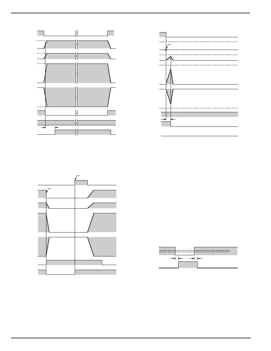
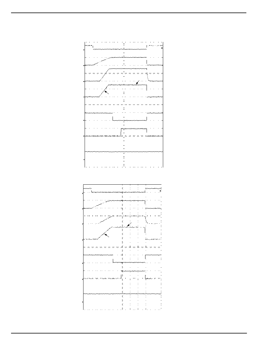
Timing Diagrams
Figure 1. Controller Timing: Normal Cycle
Figure 2. Controller Timing: Enable Into Short
Figure 3. Controller Timing: Short on 5V
/ON
+5V
0V
0V
5VOUT
+3.3V
3VOUT
0V
+12V
12VOUT
≠12V
0V
M12VOUT
/PWRGD
/FAULT
/POR
t
RESET
/ON
+5V
0V
0V
5VOUT
+3.3V
3VOUT
0V
+12V
12VOUT
≠12V
0V
M12VOUT
/PWRGD
/FAULT
Fault
Circuit Breaker
Reset
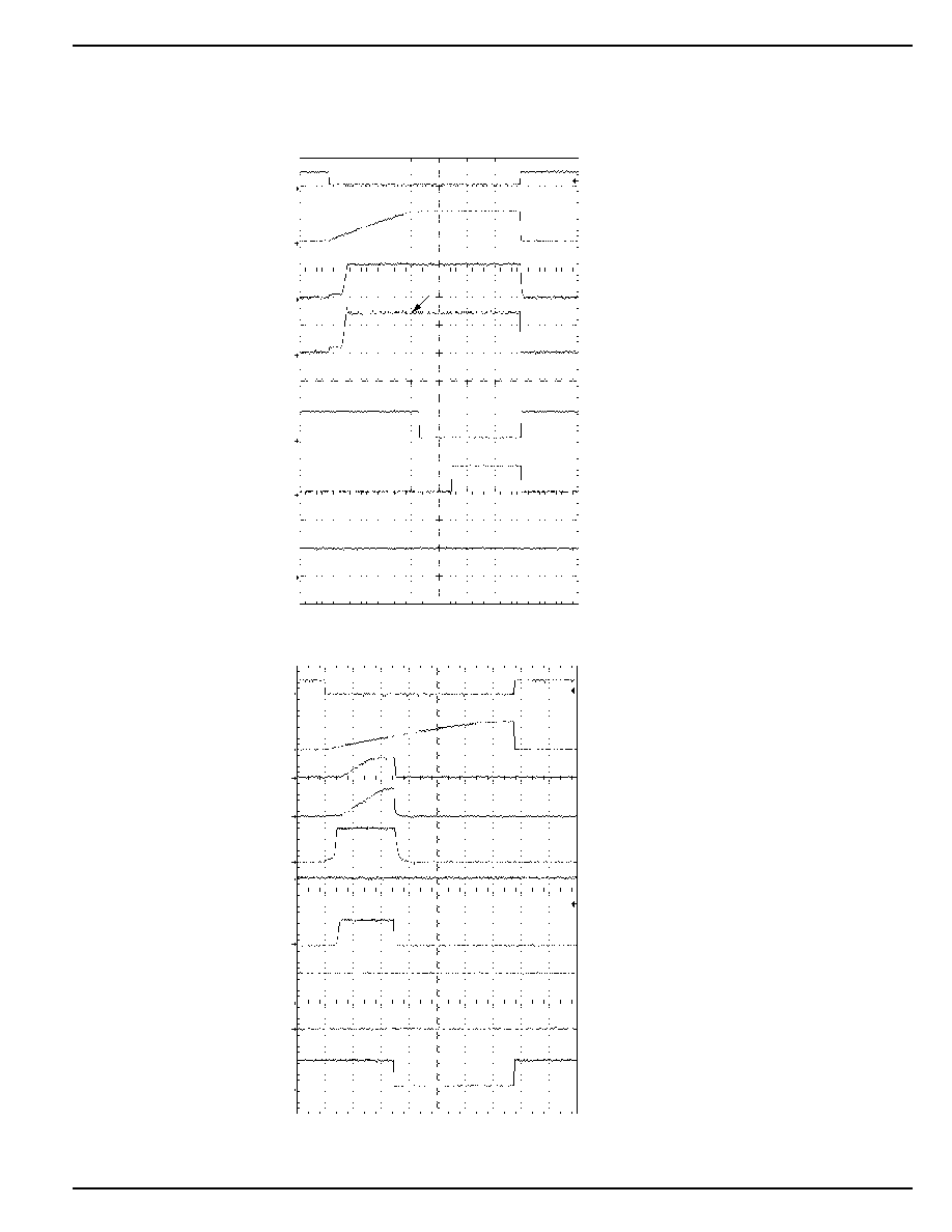
Figure 4. Early Power Good Response Time
+5V
0V
/EPWRGD
t
/good
t
good
V
IN
V
PGTH
}
1V
February 2005
7
MIC2580A
MIC2580A
Micrel, Inc.
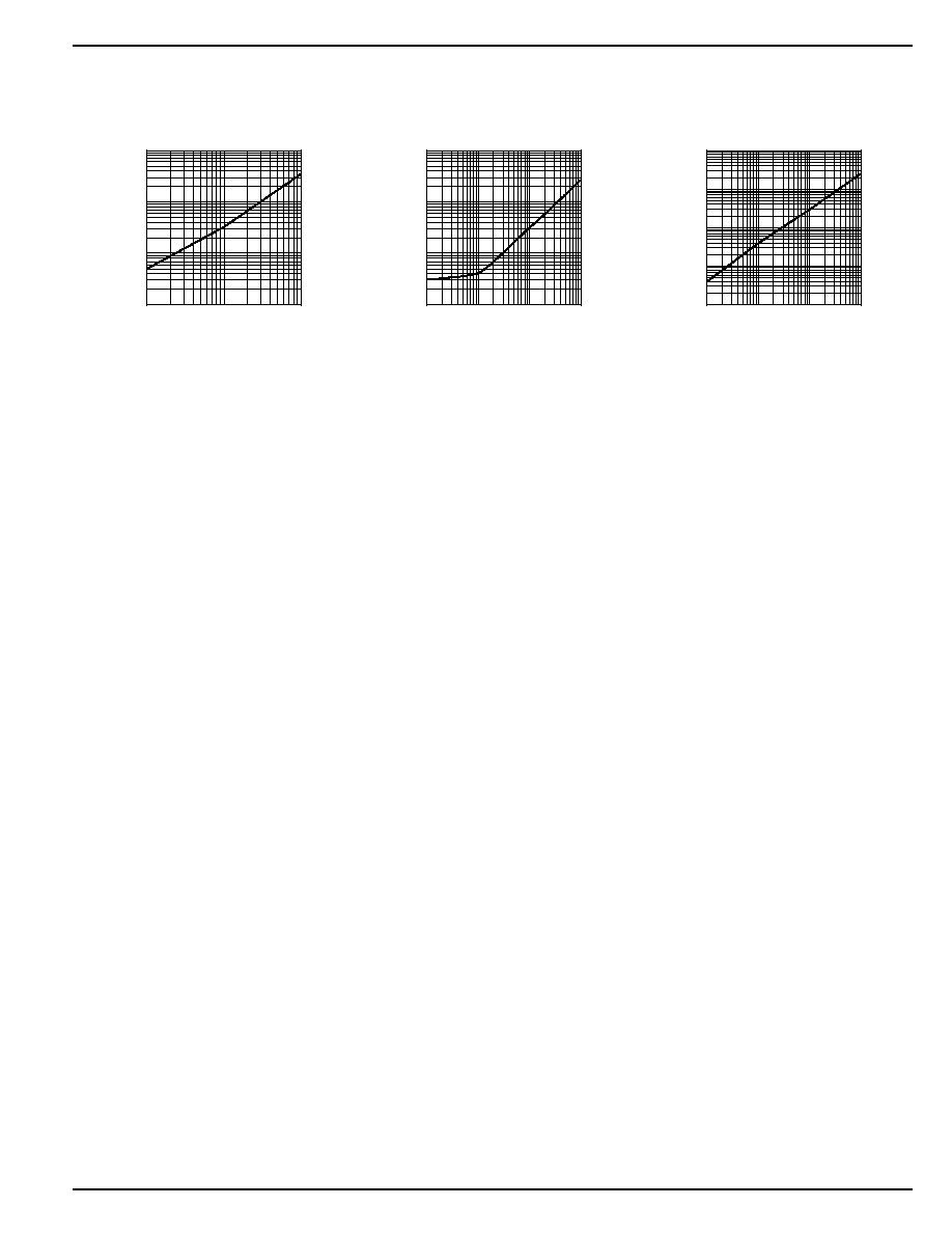
Typical Characteristics
100x10
-6
1x10
-3
10x10
-3
100x10
-3
0.001
0.01
0.1
TIME (s)
C
POR
(µF)
Power-On
Reset Time
100x10
-6
1x10
-3
10x10
-3
100x10
-3
0.0001
0.001
0.01
0.1
TIME (s)
C
SLEW
(µF)
Output Rise Time vs.
Slew-Rate Capacitance
10x10
-6
100x10
-6
1x10
-3
10x10
-3
100x10
-3
0.0001
0.001
0.01
0.1
TIME (s)
C
START
(µF)
Start-Up
Time
MIC2580A
Micrel, Inc.
MIC2580A
8
February 2005
Functional Characteristics
12VOUT
5VGATE
3VGATE
VPCHG
12VIN
/FAULT
GND
CSTART
/LPCIRST
5VIN
3VIN
/PCIRST
/EPWRGD
/ON
CSLEW
MIC2580A
5VSENSE
3VSENSE
5VOUT
3VOUT
/POR
CRST
IRF7413
IRF7413
/PWRGD
M12VIN
M12VOUT
+12V
+5V
+3.3V
2.2k
2.2k
10m
10m
C
12L
C
5L
C
3L
R
12L
R
5L
R
3L
C
RST
C
START
C
M12L
R
M12L
C
SLEW
2.2k
+5V
≠12V
2.2k
Functional Test Circuit
February 2005
9
MIC2580A
MIC2580A
Micrel, Inc.
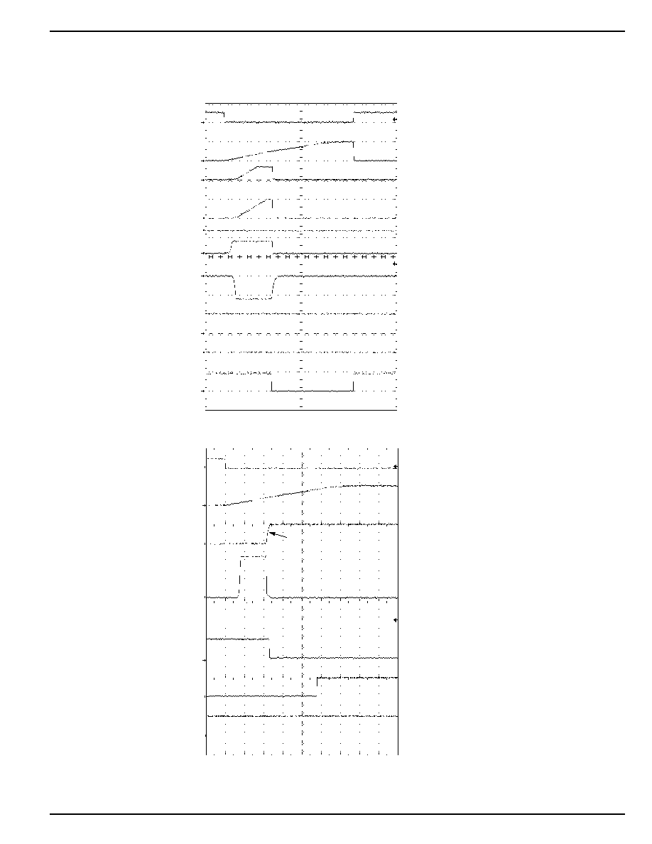
3V and 5V
Gate-Voltage Response
Time (2.5ms/div)
V
/ON
(5V/div)
V
CSLEW
(5V/div)
V
3VGATE
(5V/div)
V
5VGATE
(5V/div)
Power-On
Reset Response
t
RESET
= 2.6ms
Time (1ms/div)
V
/ON
(10V/div)
V
/PWRGD
(5V/div)
V
CRST
(2V/div)
V
/POR
(5V/div)
Power-Good
Response
Time (10µs/div)
V
/EPWRGD
(5V/div)
V
/PWRGD
(5V/div)
C
RST
= 0.01µF
C
SLEW
= 0.03µF
C
START
= 0.01µF
C
RST
= 0.01µF
MIC2580A
Micrel, Inc.
MIC2580A
10
February 2005
C
RST
= 0.01µF
Fault Response
V
/ON
(10V/div)
V
/FAULT
(10V/div)
Time (10ms/div)
V
3VOUT
(5V/div)
V
5VOUT
(5V/div)
V
12VOUT
(10V/div)
V
M12VOUT
(10V/div)
Pull /FAULT Low
February 2005
11
MIC2580A
MIC2580A
Micrel, Inc.
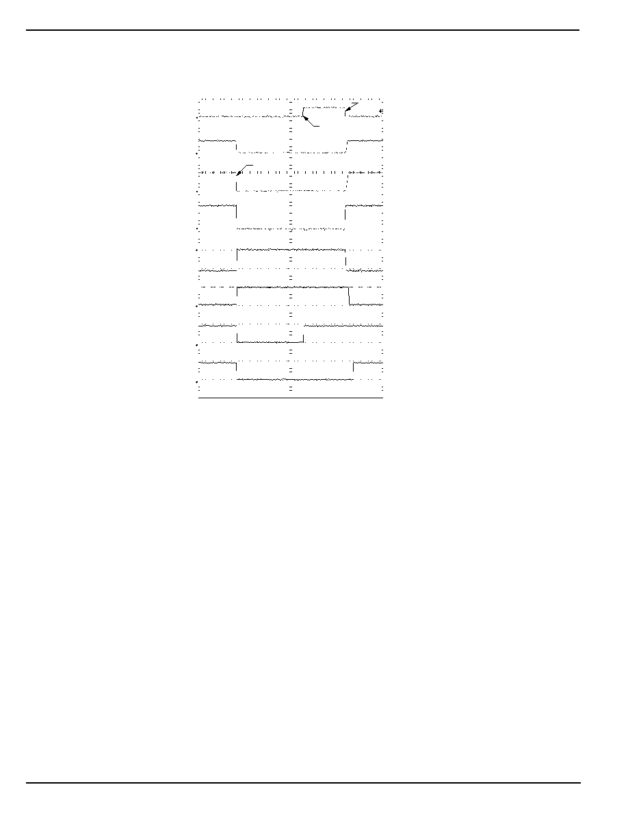
V
/PWRGD
(5V/div)
Turn-On and Turn-off
V
/ON
(10V/div)
V
3VOUT
(5V/div)
V
5VOUT
(5V/div)
V
12VOUT
(10V/div)
V
M12VOUT
(10V/div)
V
/POR
(5V/div)
V
/FAULT
(5V/div)
Time (2.5ms/div)
-12V Turn-On
V
/ON
(10V/div)
V
CSTART
(5V/div)
V
M12VOUT
(10V/div)
I
M12VIN
(100mA/div)
V
/PWRGD
(5V/div)
V
/POR
(5V/div)
V
/FAULT
(5V/div)
Time (2.5ms/div)
150mA
C
START
= 0.01µF
C
SLEW
= 0.03µF
C
RST
= 0.01µF
C
START
= 0.01µF
C
SLEW
= 0.07µF
C
RST
= 0.01µF
C
M12L
= 1µF
R
M12L
= 80
MIC2580A
Micrel, Inc.
MIC2580A
12
February 2005
3V Turn-On
V
/ON
(10V/div)
V
CSTART
(5V/div)
V
3VOUT
(2V/div)
I
3VIN
(1A/div)
V
/PWRGD
(5V/div)
V
/POR
(5V/div)
V
/FAULT
(5V/div)
Time (2.5ms/div)
1.5A
0.6A/ms
5V Turn-On
V
/ON
(10V/div)
V
CSTART
(5V/div)
V
5VOUT
(5V/div)
I
5VIN
(1A/div)
V
/PWRGD
(5V/div)
V
/POR
(5V/div)
V
/FAULT
(5V/diV)
Time (2.5ms/div)
1.5A
0.375A/ms
C
START
= 0.01µF
C
SLEW
= 0.03µF
C
RST
= 0.01µF
C
3L
= 100µF
R
3L
= 2.2
C
START
= 0.01µF
C
SLEW
= 0.03µF
C
RST
= 0.01µF
C
5L
= 100µF
R
5L
= 3.3
February 2005
13
MIC2580A
MIC2580A
Micrel, Inc.
12V Turn-On
V
/ON
(10V/div)
V
CSTART
(5V/div)
V
12VOUT
(10V/div)
I
12VIN
(100mA/div)
V
/PWRGD
(5V/div)
V
/POR
(5V/div)
V
/FAULT
(5V/div)
Time (1ms/div)
150mA
Enable Into
-12V Output Short Circuit
V
/ON
(10V/div)
V
CSTART
(5V/div)
V
3VOUT
(5V/div)
I
M12VIN
(200mA/div)
V
M12VOUT
(10V/div)
V
12VOUT
(10/div)
V
5VOUT
(5V/div)
V
/POR
(5V/div)
V
/FAULT
(5V/div)
V
/PWRGD
(5V/div)
Time (1ms/div)
C
START
= 0.01µF
C
SLEW
= 0.04µF
C
RST
= 0.01µF
C
12L
= 1µF
R
12L
= 80
C
START
= 0.01µF
C
SLEW
= 0.01µF
C
RST
= 0.01µF
R
12L
= 100
C
12L
= 1µF
M12VOUT = GND

MIC2580A
Micrel, Inc.
MIC2580A
14
February 2005
Enable Into
3V Output Short Circuit
V
/ON
(10V/div)
V
CSTART
(5V/div)
V
3VOUT
(5V/div)
V
M12VOUT
(10V/div)
V
12VOUT
(10V/div)
I
3VIN
(1A/div)
V
5VOUT
(5V/div)
V
/PWRGD
(5V/div)
V
/POR
(5V/div)
V
/FAULT
(5V/div)
Time (1ms/div)
Enable Into
5V Output Short Circuit
V
/ON
(10V/div)
V
CSTART
(5V/div)
V
3VOUT
(5V/div)
V
12VOUT
(10V/div)
V
M12VOUT
(10V/div)
V
5VOUT
(5V/div)
I
5VIN
(200mA/div)
V
/PWRGD
(5V/div)
V
/POR
(5V/div)
V
/FAULT
(5V/div)
Time (1ms/div)
C
START
= 0.01µF
C
SLEW
= 0.01µF
C
RST
= 0.01µF
3VOUT = GND
R
12L
= 100
C
12L
= 1µF
R
M12L
= 100
C
M12L
= 1µF
C
START
= 0.01µF
C
SLEW
= 0.01µF
C
RST
= 0.01µF
R
12L
= 100
C
12L
= 1µF
R
M12L
= 100
C
M12L
= 1µF
5VOUT = GND
February 2005
15
MIC2580A
MIC2580A
Micrel, Inc.
Enable Into
12V Output Short Circuit
V
/ON
(10V/div)
V
CSTART
(5V/div)
V
3VOUT
(5V/div)
V
M12VOUT
(10V/div)
V
12VOUT
(10V/div)
V
5VOUT
(5V/div)
I
12VIN
(500MA/div)
V
/PWRGD
(5V/div)
V
/FAULT
(5V/div)
Time (1ms/div)
V
/POR
(5V/div)
Start-up Blanking Response
V
/ON
(10V/div)
V
CSTART
(5V/div)
I
5VIN
(200mA/div)
V
5VOUT
(5V/div)
V
/PWRGD
(5V/div)
V
/POR
(5V/div)
V
/FAULT
(5V/div)
Time (1ms/div)
Short Removed
C
START
= 0.01µF
C
SLEW
= 0.01µF
C
RST
= 0.01µF
C
12L
= 1µF
R
M12L
= 100
C
M12L
= 1µF
12VOUT = GND
C
START
= 0.01µF
C
SLEW
= 0.01µF
C
RST
= 0.01µF
MIC2580A
Micrel, Inc.
MIC2580A
16
February 2005
Circuit Breaker
Reset Response
ON#
(10V/div)
3VOUT
(5V/div)
M12VOUT
(10V/div)
12VOUT
(10V/div)
5VOUT
(5V/div)
PWRGD#
(5V/div)
POR#
(5V/div)
FAULT#
(5V/div)
Time (10ms/div)
Circuit Breaker
New Start Cycle
Short Circuit
C
START
= 0.01µF
C
SLEW
= 0.01µF
C
RST
= 0.01µF
February 2005
17
MIC2580A
MIC2580A
Micrel, Inc.
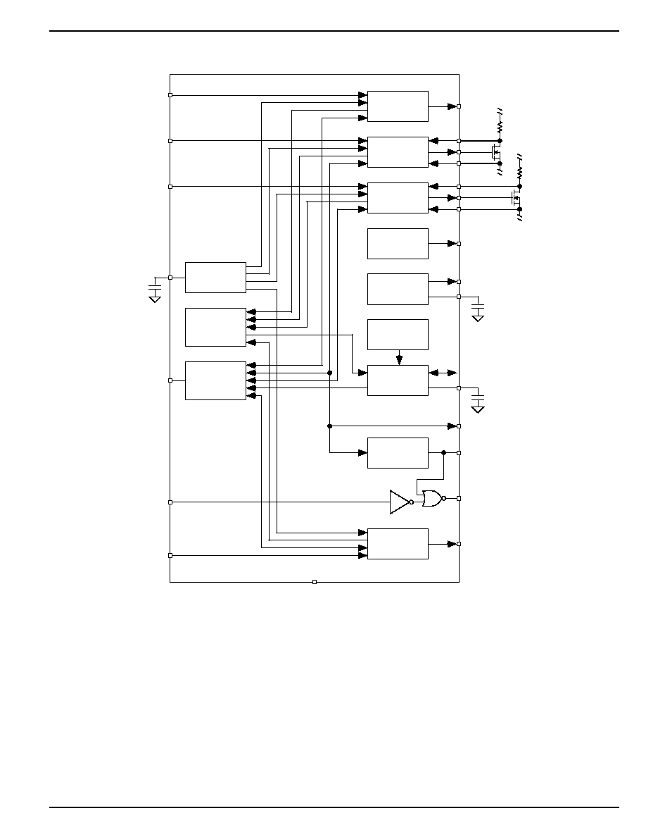
Functional Diagram
12V
Switch
5V
Switch
Control
Thermal
Shutdown
t
D
= 20µs
(delay)
≠12V
Switch
t
D
= 20µs
(delay)
Slew
Control
Current
Limit
Control Logic
and
Power Good
Precharge
Supply
3.3V
Switch
Control
12VOUT
5VGATE
3VGATE
VPCHG
12VIN
M12VOUT
/PWRGD
/LPCIRST
5VIN
3VIN
CSLEW
/ON
M12VIN
/PCIRST
MIC2580A
/EPWRGD
/FAULT
CSTART
5VSENSE
3VSENSE
5VOUT
3VOUT
/POR
GND
CRST
C
RST
C
SLEW
R
5SNS
R
3SNS
Q
5OUT
Q
3OUT
Reset
C
START
MIC2580A
Micrel, Inc.
MIC2580A
18
February 2005
Functional Description
Start-Up Sequence
The start-up sequence iniates after all four supplies are
connected to the inputs and then /ON is asserted by
transistioning from high to low. During the start-up sequence,
all four gates ramp up at a rate determined by C
SLEW
. During
this time /PWRGD is deasserted until all four supplies are
within specified levels. When /PWRGD is asserted the power-
on-reset signal /POR timer begins. The time period is defined
by C
RST
. Refer to Figure 1 for a timing diagram of the signals
during the start-up sequence.
During the start-up sequence, a current source charges
C
START
at a constant rate until a threshold voltage of 2.4V is
reached. This period of time defines an interval during which
overcurrent events are ignored. This prevents high inrush
currents that normally occur when charging capacitance
erroneously asserting /FAULT. The magnitude of the start-
up time, t
START
is defined by C
START
.
The MIC2580A employs foldback current limiting that en-
sures the device starts up in current limit. This minimizes high
inrush currents due to ramping a voltage into capacitance
regardless of the size of the load capacitance.
Overcurrent Detection
The MIC2580A senses overcurrent via the use of external
sense resistors for the 5V and 3.3V supply rails. When the
sense voltage across these resistors is greater than or equal
to 50mV an overcurrent condition is detected. Therefore the
overcurrent set point is determined by I
LIMIT
= 50mV/R
SENSE
.
For the +12V and ≠12V supply rails overcurrent detection is
set internally at 1.3A and ≠0.5A respectively.
When an overcurrent condition is detected /FAULT is as-
serted only if the overcurrent condition lasts for a minimum
time period of 10µs. This delay prevents spurious noise from
the system erroneously tripping the circuit breaker and as-
serting /FAULT. Upon /FAULT being asserted an internal
latch is set that immediately turns off all four supplies to
prevent further damage to the system. Toggling /ON will reset
the latch and initiate another start-up sequence. Figures 2
and 3 depict the timing for two fault conditions.
Thermal Shutdown
The +12V and ≠12V internal MOSFET switches are protected
by current limit and overtemperature shutdown circuitry.
When the die temperature exceeds 160∞C, /FAULT is as-
serted and all supplies are shut off. The power dissipated in
the MIC2580A is primarily due to the sum of current flowing
through the internal MOSFET switches and, to a lesser
extent, power dissipated due to the supply current. To com-
pute the total power dissipation of the MIC2580A the follow-
ing equation is used:
P
D(total)
= P
D(+12V switch)
+ P
D(≠12V switch)
+ P
D(supplies)
where:
P
D(switches)
= R
DS(on)
◊ I
OUT
2
P
D(supplies)
= V
SUPPLY
◊ I
SUPPLY
To relate this to operating junction temperature:
T
J
= P
D
◊
JA
+ T
A
where:
T
A
= ambient temperature
JA
= package thermal resistance
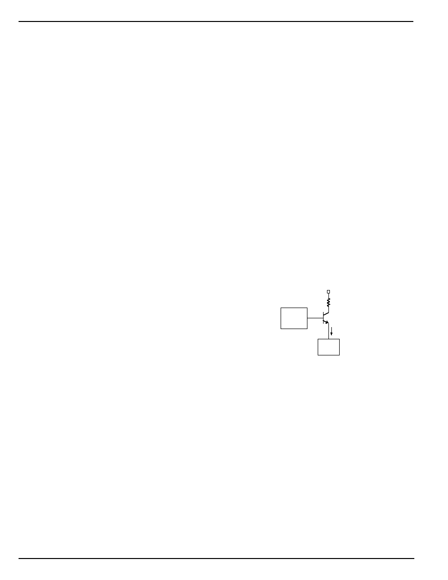
Precharge Voltage
For CompactPCI applications, the MIC2580A-1.0BSM/BTS
integrates a 1V ±20% voltage source that satisfies
CompactPCI precharge requirements. The voltage source
can provide up to 10mA. For higher current, the MIC2580A-
1.6BSM/BTS integrates a 1.6V ±20% voltage source to bias
a NPN transistor.
MIC2580A-1.6
VPCHG
DATA
BUS
R
I > 10mA
+5V
Figure 5. Voltage Source
Turnoff
Deasserting /ON will turn off all four supplies. Alternatively
driving /FAULT low will turn off all supplies but will not latch
the supplies off. Releasing /FAULT will initiate a new start
sequence.
February 2005
19
MIC2580A
MIC2580A
Micrel, Inc.
Application Information
Whenever voltage is applied to a highly capacitive load, high
inrush currents may result in voltage droop that may bring the
supply voltage out of regulation for the duration of the
transient. The MIC2580A solves this problem by specifically
controlling the current and voltage supply ramps so that the
system supply voltages are not disturbed. Very large capaci-
tive loads are easily supported with this device.
Figure 1 shows the timing during turn-on. When /ON is forced
low, all supplies are turned on at a slew rate determined by the
external capacitor, C
SLEW
.
Figure 2 shows the foldback characteristics for the supply
voltages. This foldback affect bounds the magnitude of the
current step when the supplies are turned on or shorted. This
specifies the compact PCI specification of 1.5A/ms, thereby
ensuring reliable operation. In discrete FET implementa-
tions, this magnitude can exceed several amps and may
cause the main supply to go out of regulation during this
transient event. This, in turn, could cause the system to
behave unpredictably. In addition, should a fault occur, the
MIC2580A will prevent system malfunctions by limiting the
current to within specifications.
MOSFET Selection
The external MOSFET should be selected to provide low
enough dc loss to satisfy the application's voltage regulation
requirements. Note that the voltage across the sense resistor
must also be added to the dc voltage drop across the
MOSFET to compute total loss. In addition to meeting the
voltage regulation specifications, thermal specifications must
also be considered. During normal operation very little power
should be dissipated in the MOSFET. DC power dissipation
of the MOSFET is easily computed as I
2
R
DS
where I is the
drain current and R
DS
is the specified on-resistance of the
MOSFET at the expected operating drain current. However,
during excessive drain current or short-circuit faults, the
power dissipation in the external MOSFET will increase
dramatically. To help compute the effective power dissipated
during such transients, MOSFET manufacturers provide
transient thermal impedance curves for each MOSFET.
These curves provide the effective thermal impedance of the
MOSFET under pulsed or repetitive conditions; for example,
as will be the case when enabling into a short circuit fault.
From these curves the effective rise in junction temperature
of the MOSFET for a given condition can be computed. The
equation is given as:
peak T
J
= PDM ◊ Z
JA
+ T
A
where PDM is the power dissipated in the MOSFET usually
computed as V
IN
x I
DRAIN
and Z
JA
is the thermal response
factor provided from the curves. Since the MIC2580A re-
duces the current to 30% of full scale even under severe faults
such as short-circuits the MOSFET power dissipation is held
to safe levels. This feature allows MOSFETs with smaller
packages to be used for a given application thereby reducing
cost and PCB real-estate requirements.
12VOUT
5VGATE
3VGATE
VPCHG
12VIN
/FAULT
GND
CSTART
/LPCIRST
5VIN
3VIN
/PCIRST
/EPWDGD
/ON
CSLEW
MIC2580A
5VSENSE
3VSENSE
5VOUT
3VOUT
CRST
IRF7413
IRF7413
3.3V
5V
12V
/PWDGD
M12VIN
M12VOUT
+12V
+5V
+3.3V
GND
≠12V
Power
Supply
/CIRST
BUS EN
≠12V
/CIRST
Data Bus
/CIRST
≠12V /100mA
12V/500mA
5V/5A
3.3V/7.6A
10m
10m
PCI Hot-Plug
Controller
Bus
Switch
Data Bus
GND
Adapter
Platf
o
r
m
/POR
D0
D0
+5V
D1
D1
D2
D2
Dn
Dn
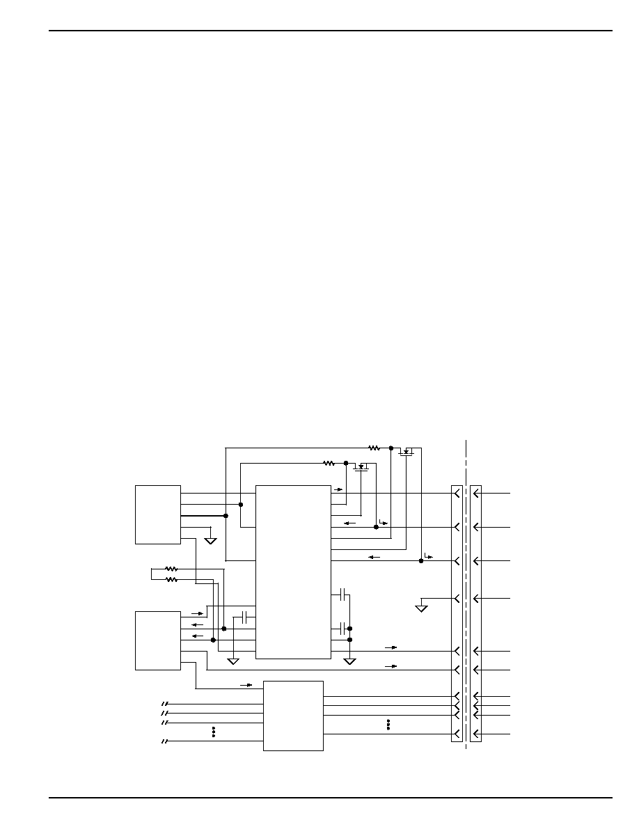
Figure 6. Hot-Plug PCI Application
MIC2580A
Micrel, Inc.
MIC2580A
20
February 2005
CompactPCITM BD_SEL# Pin Tied to Ground
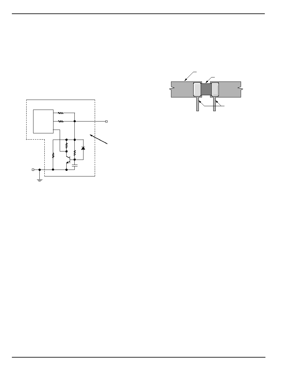
For applications that use system backplanes with the
BD_SEL# pin tied to ground, the MIC2580A /ON pin is edge
sensitive. Therefore, the /ON pin requires a delay circuit for
proper start-up when the board has already been inserted
into the backplane and the supplies are switched off, then
back on. The circuit, shown in the figure below, allows the
MIC2580A /ON pin to transition from high to low which is
necessary for start-up. The delay time may be increased or
decreased by changing the RC time constant in the circuit,
but the delay time must exceed the ramp time of all system
backplane supplies. The same circuit is functional for hot
swap insertion.
V
IO
(3.3V or 5V)
3.3µF
/FAULT
/RESET
MIC2580A
/ON
1.2k
10k
50k
2N3904
1N914
2k
2k
BD_SEL#
On PCB
Figure 7. /ON Pin Assertion Delay Circuit
PCB Layout Considerations
To achieve accurate current sensing Kelvin connections are
recommended between the supply pin and the respective
sense resistor as shown in Figure 8. PCB trace length should
be kept at a minimum. 0.02 inches per ampere is a minimum
width for 1 oz. copper to prevent damage to traces carrying
high current. Keep these high-current traces as short as
possible.
to
VIN
pin
from
supply
to
SENSE
pin
to
load
sense resistor
Kelvin
connections
short-length, high-current
(wide) copper traces
Figure 8. Layout Recommendation
February 2005
21
MIC2580A
MIC2580A
Micrel, Inc.
Package Information
1.10 MAX (0.043)
0.15 (0.006)
0.05 (0.002)
1.00 (0.039) REF
8∞
0∞
6.4 BSC (0.252)
7.90 (0.311)
7.70 (0.303)
0.30 (0.012)
0.19 (0.007)
0.20 (0.008)
0.09 (0.003)
0.70 (0.028)
0.50 (0.020)
DIMENSIONS:
MM (INCH)
4.50 (0.177)
4.30 (0.169)
0.65 BSC
(0.026)
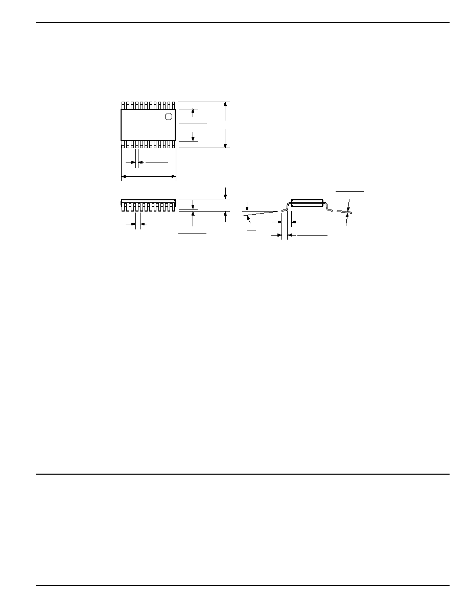
24-Lead TSSOP (TS)
MICREL INC.
2180 FORTUNE DRIVE
SAN JOSE, CA 95131
USA
TEL
+ 1 (408) 944-0800
FAX
+ 1 (408) 474-1000
WEB
http://www.micrel.com
This information furnished by Micrel in this data sheet is believed to be accurate and reliable. However no responsibility is assumed by Micrel for its use.
Micrel reserves the right to change circuitry and specifications at any time without notification to the customer.
Micrel Products are not designed or authorized for use as components in life support appliances, devices or systems where malfunction of a product can
reasonably be expected to result in personal injury. Life support devices or systems are devices or systems that (a) are intended for surgical implant into
the body or (b) support or sustain life, and whose failure to perform can be reasonably expected to result in a significant injury to the user. A Purchaser's
use or sale of Micrel Products for use in life support appliances, devices or systems is a Purchaser's own risk and Purchaser agrees to fully indemnify
Micrel for any damages resulting from such use or sale.
© 2001 Micrel Incorporated