
March 2005
1
MIC2584/2585
MIC2584/2585
Micrel
Ordering Information
Part Number
Output Sequencing
Fast Circuit Breaker
Package
Standard
Pb-Free
Threshold
MIC2584-xBTS
MIC2584-xYTS
N/A
x = J, 100mV
16-pin TSSOP
x = K, 150mV *
MIC2585-1xBTS
MIC2585-1xYTS
OUT2 follows OUT1
x = L, 200mV *24-pin TSSOP
MIC2585-2xBTS
MIC2585-2xYTS
OUT1 follows OUT2
x = M, Off *
* Contact Micrel for availability.
MIC2584/MIC2585
Dual-Channel Hot Swap Controller/Sequencer
General Description
The MIC2584 and MIC2585 are dual-channel positive volt-
age hot swap controllers designed to facilitate the safe
insertion of boards into live system backplanes. The MIC2584
and MIC2585 are available in 16-pin and 24-pin TSSOP
packages, respectively. Using a few external discrete com-
ponents and by controlling the gate drives of external N-
Channel MOSFET devices, the MIC2584/85 provides inrush
current limiting and output voltage slew rate control in harsh,
critical power supply environments. Additionally, the MIC2585
provides output turn-on sequencing and output tracking
during turn-on and turn-off. In combination, the devices'
many features provide a simplified, robust solution for many
network applications to meet the power sequencing and
protection requirements of multiple-voltage logic systems.
Features
∑ 1.0V to 13.2V supply voltage operation
∑ Surge voltage protection up to 20V
∑ Current regulation limits inrush current regardless of
load capacitance
∑ Programmable inrush current limiting
∑ Electronic circuit breaker
∑ Dual-level overcurrent fault sensing eliminates false
tripping
∑ Fast response to short circuit conditions (< 1
µ
s)
∑ Two sequenced output mode selections
(MIC2585 only)
∑
250mV supply tracking mode during turn-on/turn-off
(MIC2585 only)
∑ Overvoltage and undervoltage output monitoring
(Overvoltage for MIC2585 only)
∑ Undervoltage lockout protection
∑ /FAULT status output
∑ Power-On Reset and Power-Good status output
(Power-Good for MIC2585 only)
Applications
∑ RAID systems
∑ Network servers
∑ Base stations
∑ Network switches
∑ Hot-board insertion
Micrel, Inc. ∑ 2180 Fortune Drive ∑ San Jose, CA 95131 ∑ USA ∑ tel + 1 (408) 944-0800 ∑ fax + 1 (408) 474-1000 ∑ http://www.micrel.com
MIC2584/2585
Micrel
MIC2584/2585
2
March 2005
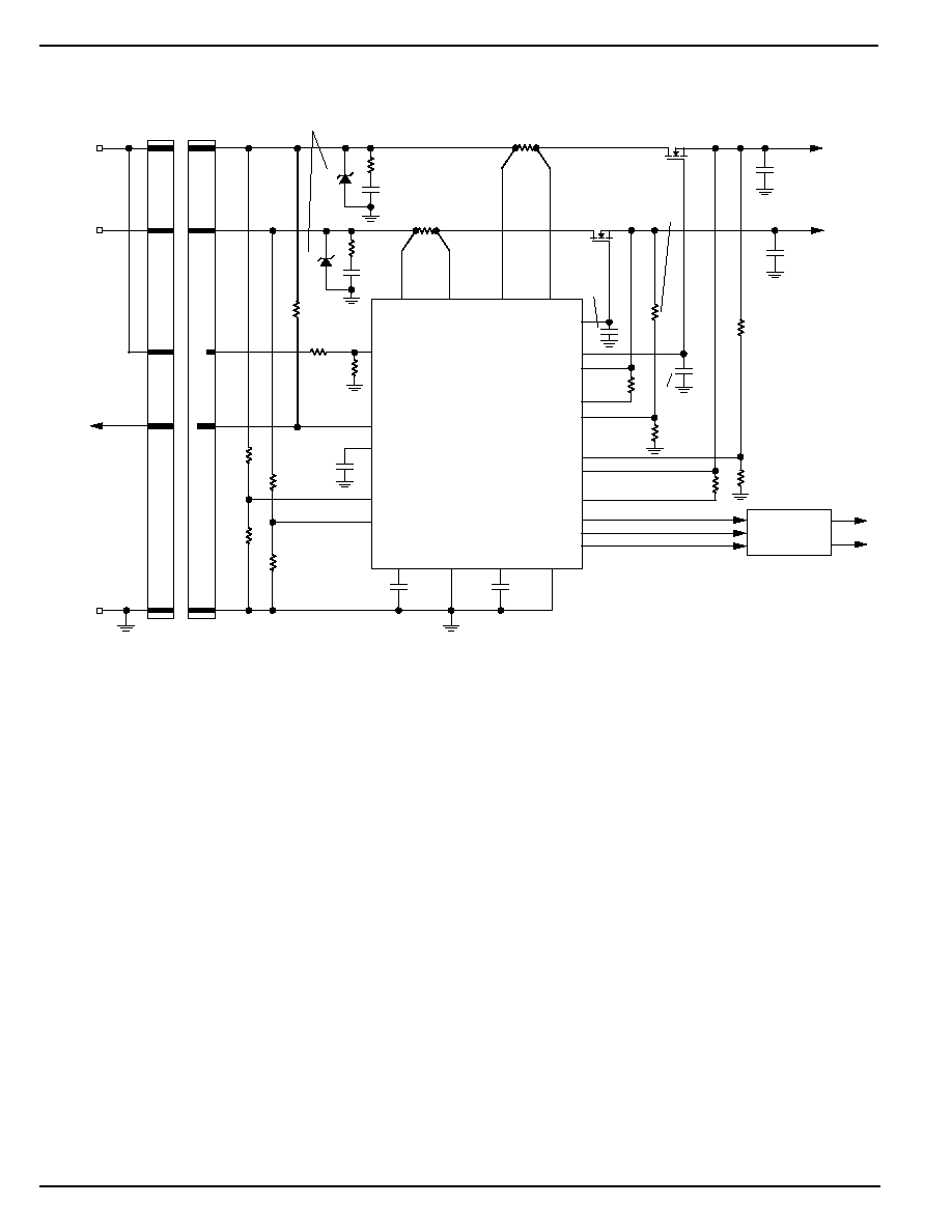
Typical Application
*C5
0.047
µ
F
D2
R6
130k
1%
R8
30.9k
1%
R9
8.06k
1%
R7
13k
1%
R3
47k
R4
22k
R2
10
R5
22k
V
CC1
12V
V
CC2
3.3V
GND
PCB EDGE
CONNECTOR
**BZX84Cxx
BACKPLANE
CONNECTOR
DOWNSTREAM
CONTROLLER(S)
Downstream Control Signals
SENSE2
VCC2
R
SENSE2
0.020
1
2
3
4
1
2
SENSE1
VCC1
R
SENSE1
0.006
1
2
3
4
24
23
C3
0.01
µ
F
Q2
Si7892DP
(PowerPAKTM SO-8)
C
LOAD1
330
µ
F
V
OUT1
12V
6A
V
OUT2
3.3V
1.5A
C
LOAD2
330
µ
F
C4
0.01
µ
F
Q1
Si7892DP
(PowerPAKTM SO-8)
C7
0.033
µ
F
C6
0.02
µ
F
CPOR
CFILTER
GND
3
22
5
6
7
20
18
19
17
16
15
11
TRK
9
13
10
GATE2
GATE1
OUT2
DIS2
DIS1
FB2
FB1
/POR
PG2
PG1
OUT1
CDLY
12
/FAULT
14
OV1
21
OV2
4
ON
8
Undervoltage (Output1) = 10.5V
Undervoltage (Output2) = 2.95V
Overvoltage (Input1) = 13.2V
Overvoltage (Input2) = 3.65V
START-UP Delay = 2.5ms
POR Delay = 10ms
Circuit Breaker Response Time = 16ms
*C5 (optional) is used to set the delay for V
OUT2
with respect to V
OUT1
V
OUT2
Delay = 9.5ms
**D1 is BZX84C18 and D2 is BZX84C8V2
Resistor tolerances are 5% unless specified otherwise.
C2
0.47
µ
F
R11
120
R15
4.42k
1%
R13
14.7k
1%
R10
560
R12
105k
1%
R14
10.7k
1%
D1
R1
10
C1
0.47
µ
F
/FAULT
Signal
MIC2585-1
Figure 1. Typical Application Circuit
March 2005
3
MIC2584/2585
MIC2584/2585
Micrel
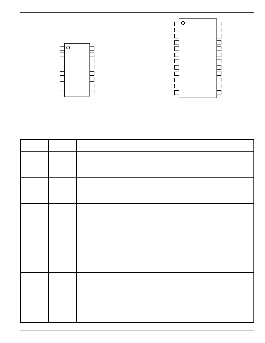
Pin Configuration
1
VCC2
SENSE2
GATE2
OUT2
FB2
ON
CPOR
CFILTER
16 VCC1
SENSE1
GATE1
OUT1
FB1
/POR
/FAULT
GND
15
14
13
12
11
10
9
2
3
4
5
6
7
8
MIC2584
16-Pin TSSOP (TS)
CDLY
GND
13
12
CFILTER
/FAULT
14
11
1
VCC2
SENSE2
GATE2
OV2
OUT2
DIS2
FB2
ON
TRK
CPOR
24 VCC1
SENSE1
GATE1
OV1
OUT1
DIS1
FB1
PG1
PG2
/POR
23
22
21
20
19
18
17
16
15
2
3
4
5
6
7
8
9
10
MIC2585
24-Pin TSSOP (TS)
Pin Description
Pin Number
Pin Number
Pin Name
Pin Function
MIC2584
MIC2585
16
24
VCC1
Positive Supply (Input), Channel 1: This input is the main supply to the
internal circuitry and must be in the range of 2.3V to 13.2V. The GATE1 pin
is held low by an internal undervoltage lockout circuit until V
CC1
and V
CC2
exceed their respective undervoltage lockout threshold of 2.165V and 0.8V.
This input is protected up to 20V.
1
1
VCC2
Positive Supply (Input), Channel 2: The GATE2 pin is held low by an
internal undervoltage lockout circuit until V
CC1
and V
CC2
exceed their
respective undervoltage lockout threshold of 2.165V and 0.8V. This input
must be in the range of 1.0V to 13.2V and less than or equal to V
CC1
. This
input is protected up to 20V.
2, 15
2, 23
SENSE2, SENSE1
Circuit Breaker Sense (Inputs): A resistor between this pin and VCC1 and
VCC2 sets the current limit threshold for each channel. Whenever the
voltage across either sense resistor exceeds the slow trip current limit
threshold (V
TRIPSLOW
), the GATE voltage is adjusted to ensure a constant
load current. If V
TRIPSLOW
(50mV) is exceeded for longer than time period
t
OCSLOW
, then the circuit breaker is tripped and both GATE outputs are
immediately pulled low. If the voltage across either sense resistor exceeds
the fast trip circuit breaker threshold, V
TRIPFAST
, at any point due to fast,
high amplitude power supply faults, then both GATE outputs are immediately
brought low without delay. To disable the circuit breaker for either channel,
the SENSE and VCC pins can be tied together.
The default V
TRIPFAST
for either device is 100mV. Other fast trip thresholds
are available: 150mV, 200mV, or OFF (V
TRIPFAST
disabled). Please contact
factory for availability of other options.
6
8
ON
Enable (Input): Active High. The ON pin, an input to a Schmitt-triggered
comparator used to enable/disable the controller, is compared to a 1.235V
reference with 25mV of hysteresis. When a logic high is applied to the ON
pin (V
ON
> 1.235V), a start-up sequence begins when the GATE1 and
GATE2 pins begin ramping up towards their final operating voltage. When
the ON pin receives a logic low signal (V
ON
< 1.21V), the GATE pins are
grounded and /FAULT remains high if both inputs are above their respective
UVLO thresholds. The ON pin must be low for at least 20
µ
s in order to
initiate a start-up sequence. Additionally, toggling the ON pin LOW to HIGH
resets the circuit breaker.

MIC2584/2585
Micrel
MIC2584/2585
4
March 2005
Pin Number
Pin Number
Pin Name
Pin Function
MIC2584
MIC2585
3, 14
3, 22
GATE2, GATE1
Gate Drive (Outputs): Connect each output to the gates of external
N-Channel MOSFETs. When ON is asserted, a 14
µ
A current source is
activated and begins to charge the gate of the N-Channel MOSFET connected
to this pin. An internal clamp ensures that no more than 10V is applied
between the GATE and Source when VCC1 or VCC2 is above 5V. When the
circuit breaker trips or when an input undervoltage lockout condition is
detected, the GATE1 and GATE2 pins are immediately brought low.
9
13
GND
Ground: Tie to analog ground.
7
10
CPOR
Power-On Reset Timer (Input): A capacitor connected between this pin and
ground sets the start-up delay (t
START
) and the power-on reset interval
(t
POR
). Once the lagging supply rises above its UVLO threshold and ON
asserts, the capacitor connected to CPOR begins to charge. When the
voltage at CPOR crosses 0.3V, the start-up threshold (V
START
), a start cycle
is initiated as the GATE outputs begin to ramp while capacitor C
POR
is
immediately discharged to ground. When the voltage at the lagging FB pin
rises above its threshold (V
FB
), capacitor CPOR begins to charge again.
When the voltage at CPOR rises above the power-on reset delay threshold
(V
POR
) of 1.235V, the timer resets by pulling CPOR to ground and /POR is
deasserted. If C
POR
= 0, then t
START
defaults to 20
µ
s.
8
11
CFILTER
Current Limit Response Timer (Input): A capacitor connected to this pin
defines the period of time, t
OCSLOW
, in which an overcurrent event must last
to signal a fault condition and trip the circuit breaker. When an overcurrent
condition occurs, a 2.5
µ
A current source begins to charge this capacitor. If
the voltage at this pin reaches 1.235V, the circuit breaker is tripped, both
GATE pins immediately shut off, and /FAULT is asserted. If C
FILTER
= 0,
then t
OCSLOW
defaults to 20
µ
s.
5, 12
7, 18
FB2, FB1
Power-Good Threshold Input (Undervoltage Detect): FB1 and FB2 are
internally compared to 1.235V and 0.80V references with 25mV of hyster-
esis, respectively. External resistive divider networks may be used to set the
voltage at these pins. If either FB input momentarily goes below its thresh-
old, then /POR is activated for one timing cycle, t
POR
, indicating an output
undervoltage condition. The /POR signal deasserts one timing cycle after the
FB pin exceeds its power-good threshold by 25mV. A 5
µ
s filter on these pins
prevents glitches from inadvertently activating the /POR signal.
10
14
/FAULT
Circuit Breaker Fault Status (Output): Active-Low, weak pull-up to VCC1 or
open-drain. Asserted when the circuit breaker is tripped due to an
overcurrent, undervoltage lockout, or overvoltage event. When deasserted,
the MIC2585 will initiate a new start cycle by toggling the ON pin.
11
15
/POR
Power-On Reset (Output): Active Low, weak pull-up to VCC1 or open drain.
This pin remains asserted during start-up until a time period (t
POR
) after the
lagging FB pin threshold (V
FB1
or V
FB2
) is exceeded. The timing capacitor
C
POR
determines t
POR
. When the output voltage monitored at either FB pin
falls below V
FB
, /POR is asserted for a minimum of one timing cycle (t
POR
).
4, 13
5, 20
OUT2, OUT1
Output Voltage Monitor (Inputs): For output tracking, connect these pins to
their respective output to sense the output voltage.
N/A
12
CDLY
Output Sequence Delay Timer (Input): This pin is internally clamped to 6V.
A capacitor connected to this pin sets a timer delay, t
DLY
, between V
OUT1
and V
OUT2
as shown in Figure 5. With this pin pulled up to VCC1 through a
resistor, and if C
GATE1
= C
GATE2
, both V
OUT1
and V
OUT2
ramp up and down
with the same dv/dt as depicted in the Tracking Mode diagram while
maintaining a maximum voltage differential between V
OUT1
and V
OUT2
.
N/A
9
TRK
Discharge Tracking Mode Pin (Input): Tie this pin to OUT1 or OUT2 to
enable tracking during turn-off cycle. Ground this pin to disable tracking
during turn-off. The TRK pin is not to be used as a digital input.

March 2005
5
MIC2584/2585
MIC2584/2585
Micrel
Pin Number
Pin Number
Pin Name
Pin Function
MIC2584
MIC2585
N/A
4, 21
OV2, OV1
Overvoltage Detect Inputs: Whenever the threshold voltage (V
OV1
, V
OV2
) on
either input is exceeded, the circuit-breaker is tripped while /FAULT is
asserted and the GATE1 and GATE2 outputs are immediately brought low.
N/A
6, 19
DIS2, DIS1
Discharge Outputs: When the ON pin receives a logic low signal
(deasserts), these pins provide a low impedance path to ground in order to
allow the discharging of any load capacitance. The DIS pins assert low if
TRK is less than 0.3V once ON has been deasserted. The typical DIS pin
resistance varies between 50
to 170
dependent upon input supply
voltage (see Electrical Table). An external resistor is required. See "
Fast
Output Discharge for Capacitive Load
" section in the Applications Informa-
tion for more detail.
N/A
16, 17
PG2, PG1
Power-Good Outputs: Active-HIGH, weak pull-up to VCC1 or open-drain.
These outputs are asserted whenever the FB1 and FB2 thresholds are
exceeded and will not be asserted when FB1 and FB2 are below their
thresholds.
MIC2584/2585
Micrel
MIC2584/2585
6
March 2005
Absolute Maximum Ratings
(Note1)
All voltages are referred to GND)
Supply Voltage (V
CC1
/V
CC2
) .......................... ≠0.3V to 20V
SENSE1/SENSE2 pins .............................. ≠0.3V to V
CC1/2
TRK, ON, DIS1, DIS2, OUT1, OUT2,
/POR, /FAULT, PG1, PG2 pins .................. ≠0.3V to 15V
GATE1/GATE2 pin ......................................... ≠0.3V to 25V
All other input pins ........................................... -0.3V to 15V
DIS1/DIS2 current ....................................................
±
25mA
Junction Temperature ............................................... 125
∞
C
ESD Rating
Human body model ............................................... 1500V
Machine model ........................................................ 100V
Operating Ratings
(Note 2)
Supply Voltage
V
CC1 .........................................................................
2.3V to 13.2V
V
CC2 .........................................................................
1.0V to 13.2V
Operating Temperature Range .................. ≠40
∞
C to +85
∞
C
Package Thermal Resistance
R
(
JA)
, 16-pin TSSOP ....................................... 99.1
∞
C/W
R
(
JA)
, 24-pin TSSOP ....................................... 83.8
∞
C/W
Electrical Characteristics
(Note 4)
2.3V
V
CC1
13.2V, 1.0V
V
CC2
13.2V, T
A
= 25
∞
C unless otherwise noted. Bold values indicate ≠40
∞
C
T
A
85
∞
C.
Symbol
Parameter
Condition
Min
Typ
Max
Units
V
CC1
Supply Voltage
2.3
13.2
V
I
CC1
Supply Current
1.7
3
mA
V
CC2
Supply Voltage
V
CC2
V
CC1
1.0
13.2
V
I
CC2
Supply Current
0.05
0.15
mA
V
UV1
V
CC1
Undervoltage Lockout
2.050
2.165
2.275
V
Threshold
V
UV1HYS
V
CC1
Undervoltage Lockout
200
mV
Hysteresis
V
UV2
V
CC2
Undervoltage Lockout
0.7
0.8
0.9
V
Threshold
V
UV2HYS
V
CC2
Undervoltage Lockout
30
mV
Hysteresis
V
TRIPSLOW
Slow Trip Overcurrent Threshold
V
CCx
≠ V
SENSEx
, V
CC1
= V
CC2
= 5V
42.5
50
57.5
mV
V
TRIPHYS
Slow Trip Overcurrent Hysteresis
2.5
mV
V
TRIPFAST
Fast Trip Overcurrent Threshold
x = J
90
100
110
mV
V
CC1
= V
CC2
= 5V
x = K
150
mV
x = L
200
mV
V
GATE
External Gate Drive
V
GATEx
≠ V
CCx
V
CC1
or V
CC2
> 5V
6
8
10
V
(GATE1 and GATE2)
V
CC1
or V
CC2
< 5V
3.5
4.5
8
V
I
GATE
GATE Pin Pull-up Current
Start cycle
≠25
≠14
≠8
µ
A
I
GATEOFF
GATE Pin Sink Current
/FAULT asserted
50
mA
Turn off (ON deasserted)
30
45
70
µ
A
R
DIS
Discharge Pin Resistance
ON deasserted
V
CCx
= 2.3V
170
TRK < 0.3V
V
CCx
= 5.0V
70
V
CCx
= 13.2V
50
I
TMR
Overcurrent Timer Pin Charge
V
CCx
≠ V
SENSEx
= 50mV
≠3.5
≠2.5
≠1.5
µ
A
Current
Overcurrent Timer Pin Discharge
V
CCx
≠ V
SENSEx
= 25mV
1.5
2.5
3.5
µ
A
Current
V
TMR
Overcurrent Timer Pin Threshold
1.190
1.235
1.290
V

March 2005
7
MIC2584/2585
MIC2584/2585
Micrel
Symbol
Parameter
Condition
Min
Typ
Max
Units
I
CPOR
Power-on Reset Current
V
CC1
= 5V, C
POR
= 0.5V
Charge current
≠3.5
≠2.5
≠1.5
µ
A
Sink current
2.5
V
POR
Power-on Reset Delay Threshold
Start-up cycle
1.190
1.235
1.290
V
V
PORHYS
Power-on Reset Delay Threshold
25
mV
Hysteresis
V
START
Start-up Threshold
Start-up cycle
0.25
0.30
0.35
V
V
TRK
TRK Pin Threshold
ON deasserted, I
GATE
> 10
µ
A
0.25
0.30
0.35
V
(MIC2585 only)
V
CC1
= V
CC2
= 5V
V
TRKOFF
TRK Pin Turn-off Voltage
ON asserted, V
SENSE2
≠ V
OUT2
150
250
400
mV
(MIC2585 only)
V
CC1
= V
CC2
= 5V
V
FB1
FB1 Threshold
1.190
1.235
1.290
V
V
FB1HYS
FB1 Threshold Hysteresis
25
mV
V
FB2
FB2 Threshold
0.75
0.80
0.85
V
V
FB2HYS
FB2 Threshold Hysteresis
25
mV
V
OV1
OV1 Threshold
1.190
1.235
1.290
V
(MIC2585 only)
V
OV1HYS
OV1 Threshold Hysteresis
25
mV
(MIC2585 only)
V
OV2
OV2 Threshold
0.75
0.80
0.85
V
(MIC2585 only)
V
OV2HYS
OV2 Threshold Hysteresis
25
mV
(MIC2585 only)
I
DELAY
Delay Timer Pin Current
V
CC1
= V
CC2
= 5V
Timer charge current
≠9
≠6
≠3
µ
A
(MIC2585 only)
Timer discharge current
200
V
DELAY
Delay Timer Pin Threshold
1.190
1.235
1.290
V
(MIC2585 only)
V
DLYHYS
Delay Timer Pin Threshold
25
mV
Hysteresis (MIC2585 only)
V
ON
ON Pin Input Threshold
1.190
1.235
1.290
V
V
ONHYS
ON Pin Hysteresis
25
mV
I
ON
ON Pin Input Current
V
ON
= V
CCX
0.1
0.5
µ
A
V
OL
/FAULT , /POR , PG1, PG2 Output
I
OUT
= 1.6mA, V
CC1
= 5V
0.4
V
Low Voltage (PG1 and PG2 for
MIC2585 only)
I
PULLUP
/FAULT , /POR , PG1, PG2 Active
ON asserted, V
FB1
> 1.25V, V
FB2
> 0.8V
7
12
22
µ
A
Output Pull-up Current
/POR = V
CC1
≠ 1V
(PG1 and PG2 for MIC2585 only)
V
GATEWIN
GATE1 and GATE2 ON/OFF
See Timing Diagram (Figure 2)
100
250
mV
Voltage Window (Tracking enabled)
Note 3
AC Parameters
t
OCFAST
Fast Overcurrent Sense to GATE
V
CCx
≠ V
SENSEx
= 100mV, C
GATE
= 10nF
1
µ
s
Low Trip Time
See Timing Diagram (Figure 3)
t
OCSLOW
Slow Overcurrent Sense to GATE
V
CCx
≠ V
SENSEx
= 50mV, C
FILTER
= 0
20
µ
s
Low Trip Time
Note 1.
Exceeding the absolute maximum rating may damage the device.
Note 2.
The device is not guaranteed to function outside its operating rating.
Note 3.
For the MIC2584, V
GATEWIN
is specified only when ON is asserted.
Note 4.
Specification for packaged product only.

MIC2584/2585
Micrel
MIC2584/2585
8
March 2005
Timing Diagrams
ON
100mV
OFF
VOUT1 - VOUT2
ON Pin Asserted
GATE2
GATE1
ON Pin Deasserted
VOUT1 - VOUT2
ON
OFF
GATE1 ON
GATE2 ON
GATE1 OFF
GATE2 ON
GATE1 ON
GATE2 OFF
GATE1 OFF
GATE2 OFF
GATE1 OFF
GATE2 ON
GATE1 ON
GATE2 OFF
100mV
Figure 2. Gate Voltage Window -- Tracking Mode
0.5V
50mV
V
GATEx
t
OCSLOW
V
TRIPFAST
(V
CCx
≠ V
SENSEx
)
t
OCFAST
0.5V
Figure 3. Current Limit Response
ON
CPOR
t
POR
t
START
V
OUT[1,2]
V
PG[1/2]
PG
[1/2]
/POR
V
POR
V
START
Figure 4. Start-Up Cycle Timing
V
OUT1
V
OUT2
V<0.25V
V<0.25V
Tracking Mode, TRK = V
OUT1
or V
OUT2
Sequencing/Tracking Mode, TRK = V
OUT1
or V
OUT2
(-1) - V
OUT2
follows V
OUT1
(-2) - V
OUT1
follows V
OUT2
V
OUT1
,
(-1)
V
OUT2
(-2)
V
OUT2
,
(-1)
V
OUT1
(-2)
V<0.25V
V
FB
t
DLY
Figure 5. Sequencing Modes (MIC2585 only)

March 2005
9
MIC2584/2585
MIC2584/2585
Micrel
Typical Characteristics
42
44
46
48
50
52
54
56
58
-40 -20
0
20
40
60
80 100
V
TRIPSLOW1+
(mV)
TEMPERATURE (
∞
C)
V
TRIPSLOW1+
vs. Temperature
V
CC1
= 5.0V
V
CC1
= 13.2V
V
CC1
= 2.3V
42
44
46
48
50
52
54
56
58
-40 -20
0
20
40
60
80 100
V
TRIPSLOW1
≠
(mV)
TEMPERATURE (
∞
C)
V
TRIPSLOW1≠
vs. Temperature
V
CC1
= 5.0V
V
CC1
= 13.2V
V
CC1
= 2.3V
42
44
46
48
50
52
54
56
58
-40 -20
0
20
40
60
80 100
V
TRIPSLOW2+
(mV)
TEMPERATURE (
∞
C)
V
TRIPSLOW2+
vs. Temperature
V
CC2
= 5.0V
V
CC2
= 13.2V
V
CC2
= 2.3V
V
CC2
= 1.0V
42
44
46
48
50
52
54
56
58
-40 -20
0
20
40
60
80 100
V
TRIPSLOW2
≠
(mV)
TEMPERATURE (
∞
C)
V
TRIPSLOW2≠
vs. Temperature
V
CC2
= 5.0V
V
CC2
= 13.2V
V
CC2
= 2.3V
V
CC2
= 1.0V
90
92
94
96
98
100
102
104
106
108
110
-40 -20
0
20
40
60
80 100
V
TRIPFAST1
(mV)
TEMPERATURE (
∞
C)
V
TRIPFAST1
vs. Temperature
V
CC1
= 5.0V
V
CC1
= 13.2V
V
CC1
= 2.3V
90
92
94
96
98
100
102
104
106
108
110
-40 -20
0
20
40
60
80 100
V
TRIPFAST2
(mV)
TEMPERATURE (
∞
C)
V
TRIPFAST2
vs. Temperature
V
CC2
= 5.0V
V
CC2
= 13.2V
V
CC2
= 2.3V
5
7.5
10
12.5
15
17.5
20
22.5
-40 -20
0
20
40
60
80 100
GATE VOLTAGE_1 (V)
TEMPERATURE (
∞
C)
V
GATE1
vs. Temperature
V
CC1
= 5.0V
V
CC1
= 13.2V
V
CC1
= 2.3V
5
7.5
10
12.5
15
17.5
20
22.5
-40 -20
0
20
40
60
80 100
GATE VOLTAGE_2 (V)
TEMPERATURE (
∞
C)
V
GATE2
vs. Temperature
V
CC2
= 5.0V
V
CC2
= 13.2V
V
CC2
= 2.3V
0.5
0.75
1
1.25
1.5
1.75
2
2.25
2.5
-40 -20
0
20
40
60
80 100
UVLO THRESHOLD (V)
TEMPERATURE (
∞
C)
UVLO1 and UVLO2
vs. Temperature
UVLO1+
UVLO1≠
UVLO2+
UVLO2≠
1.2
1.21
1.22
1.23
1.24
1.25
1.26
-40 -20
0
20
40
60
80 100
OVERCURRENT TIMER (V)
TEMPERATURE (
∞
C)
Overcurrent Timer Threshold
vs. Temperature
V
CC
= 13.2V
V
CC
= 5.0V
V
CC
= 2.3V
0.27
0.28
0.29
0.3
0.31
0.32
-40 -20
0
20
40
60
80 100
CPOR THRESHOLD1 (V)
TEMPERATURE (
∞
C)
CPOR Threshold1 (Start-Up)
vs. Temperature
V
CC1
= 13.2V
V
CC1
= 5.0V
V
CC1
= 2.3V
1.2
1.22
1.24
1.26
1.28
1.3
-40 -20
0
20
40
60
80 100
CPOR THRESHOLD2 (V)
TEMPERATURE (
∞
C)
CPOR Threshold2
vs. Temperature
V
CC2
= 13.2V
V
CC2
= 5.0V
V
CC2
= 2.3V

MIC2584/2585
Micrel
MIC2584/2585
10
March 2005
1.21
1.22
1.23
1.24
1.25
-40 -20
0
20
40
60
80 100
OVERVOLTAGE1 (V)
TEMPERATURE (
∞
C)
Overvoltage1
vs. Temperature
V
CC1
= 13.2V
V
CC1
= 5.0V
V
CC1
= 2.3V
0.71
0.73
0.75
0.77
0.79
0.81
0.83
0.85
-40 -20
0
20
40
60
80 100
OVERVOLTAGE2 (V)
TEMPERATURE (
∞
C)
Overvoltage2
vs. Temperature
V
CC2
= 13.2V
V
CC2
= 5.0V
V
CC2
= 2.3V
1.2
1.21
1.22
1.23
1.24
1.25
-40 -20
0
20
40
60
80 100
FB1 THRESHOLD (V)
TEMPERATURE (
∞
C)
FB1 Threshold
vs. Temperature
V
CC1
=13.2V
V
CC1
=5.0V
V
CC1
=2.3V
FB1+
FB1≠
V
CC1
=13.2V
V
CC1
=5.0V
V
CC1
=2.3V
0.71
0.73
0.75
0.77
0.79
0.81
-40 -20
0
20
40
60
80 100
FB2 THRESHOLD (V)
TEMPERATURE (
∞
C)
FB2 Threshold
vs. Temperature
FB2+
FB2≠
V
CC2
=13.2V
V
CC2
=2.3V
V
CC2
=5.0V
V
CC2
=13.2V
V
CC2
=2.3V
V
CC2
=5.0V
0
0.1
0.2
0.3
0.4
-40 -20
0
20
40
60
80 100
OUTPUT LOW VOLTAGE (V)
TEMPERATURE (
∞
C)
Output Low Voltage
vs. Temperature
V
CC
= 2.3V
V
CC
= 13.2V
V
CC
= 5.0V
8
10
12
14
16
18
20
22
24
-40 -20
0
20
40
60
80 100
GATE1 ON CURRENT (
µ
A)
TEMPERATURE (
∞
C)
Gate1 On Current
vs. Temperature
V
CC
= 2.3V
V
CC
= 13.2V
V
CC
= 5.0V
2.2
2.3
2.4
2.5
2.6
2.7
2.8
-40 -20
0
20
40
60
80 100
OVERCURRENT TIMER CURRENT (
µ
A)
TEMPERATURE (
∞
C)
Overcurrent Timer
Discharge Current
vs. Temperature
V
CC
= 2.3V
V
CC
= 13.2V
V
CC
= 5.0V
-2.1
-2.2
-2.3
-2.4
-2.5
-2.6
-2.7
-2.8
-2.9
-40 -20
0
20
40
60
80 100
OVERCURRENT TIMER CURRENT (
µ
A)
TEMPERATURE (
∞
C)
Overcurrent Timer
Charge Current
vs. Temperature
V
CC
= 2.3V
V
CC
= 13.2V
V
CC
= 5.0V
2.4
2.5
2.6
2.7
2.8
-40 -20
0
20
40
60
80 100
POWER ON RESET CURRENT (
µ
A)
TEMPERATURE (
∞
C)
Power On Reset Current
vs. Temperature
V
CC
= 2.3V
V
CC
= 13.2V
V
CC
= 5.0V
2.4
2.5
2.6
2.7
2.8
-40 -20
0
20
40
60
80 100
ACTIVE OUTPUT PULL-UP CURRENT (
µ
A)
TEMPERATURE (
∞
C)
Active Output Pull-Up Current
vs. Temperature
V
CC
= 2.3V
V
CC
= 13.2V
V
CC
= 5.0V
0
0.5
1
1.5
2
2.5
3
-40 -20
0
20
40
60
80 100
SUPPLY CURRENT_1 (mA)
TEMPERATURE (
∞
C)
Supply Current_1
vs. Temperature
V
CC1
= 2.3V
V
CC1
= 13.2V
V
CC1
= 5.0V
20
30
40
50
60
70
80
90
100
110
120
-40 -20
0
20
40
60
80 100
SUPPLY CURRENT_2 (
µ
A)
TEMPERATURE (
∞
C)
Supply Current_2
vs. Temperature
V
CC2
= 2.3V
V
CC2
= 13.2V
V
CC2
= 5.0V
March 2005
11
MIC2584/2585
MIC2584/2585
Micrel
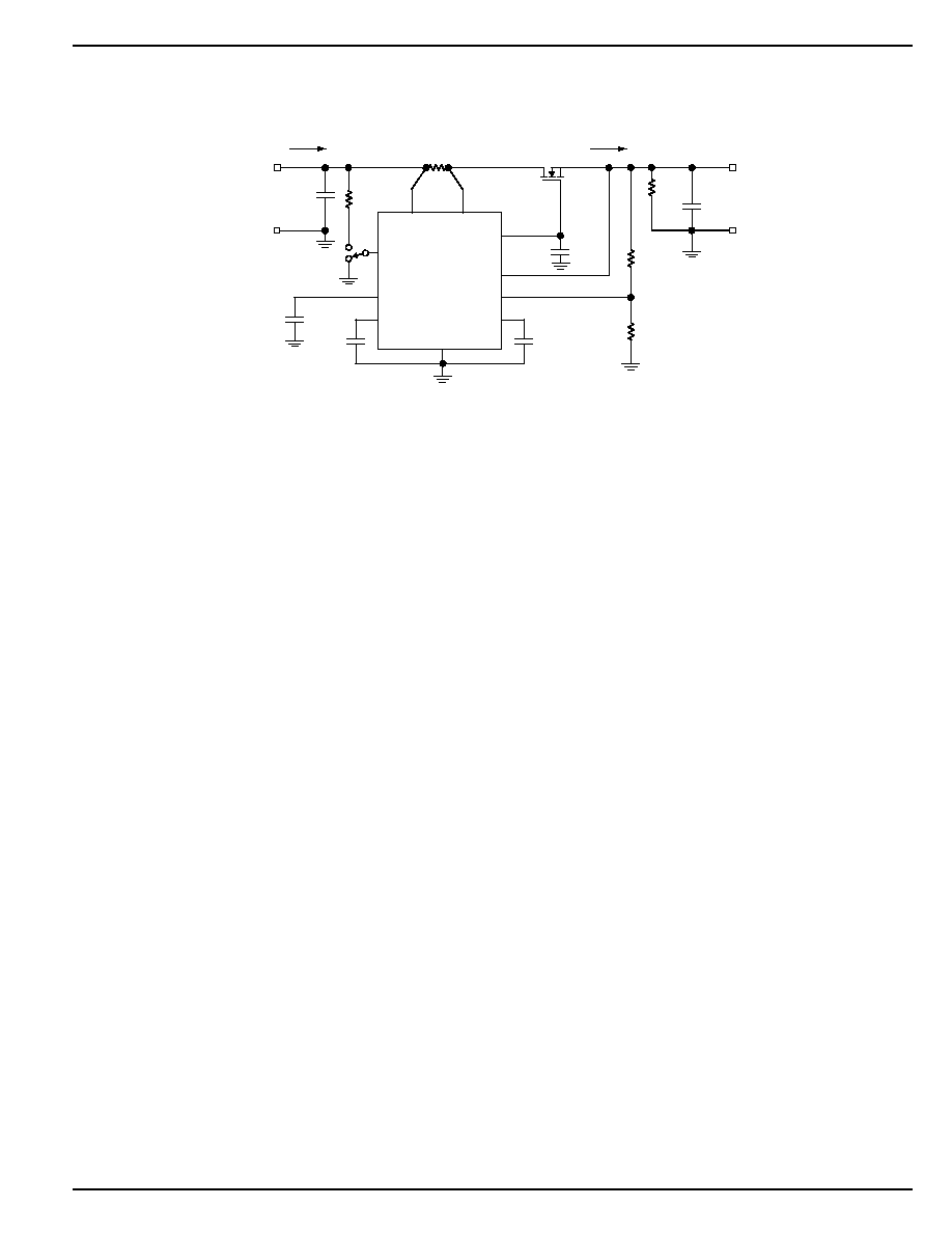
Test Circuit
V
OUTx
+
V
OUTx
≠
MIC2585
VCCx
GATEx
SENSEx
ON
CDLY
CFILTER
CPOR
GND
IRF7822
(SO-8)
I
IN
V
INx
+
V
INx
≠
C
DLY
(optional)
C
INx
4.7
µ
F
R1
R
LOAD
C
LOAD
R2
0.01
µ
F
8200pF
(Not all pins shown for simplicity)
0.1
µ
F
OUTx
FBx
33k
I
OUT
R
SENSEx
0.005
1
2
3
4
MIC2584/2585
Micrel
MIC2584/2585
12
March 2005
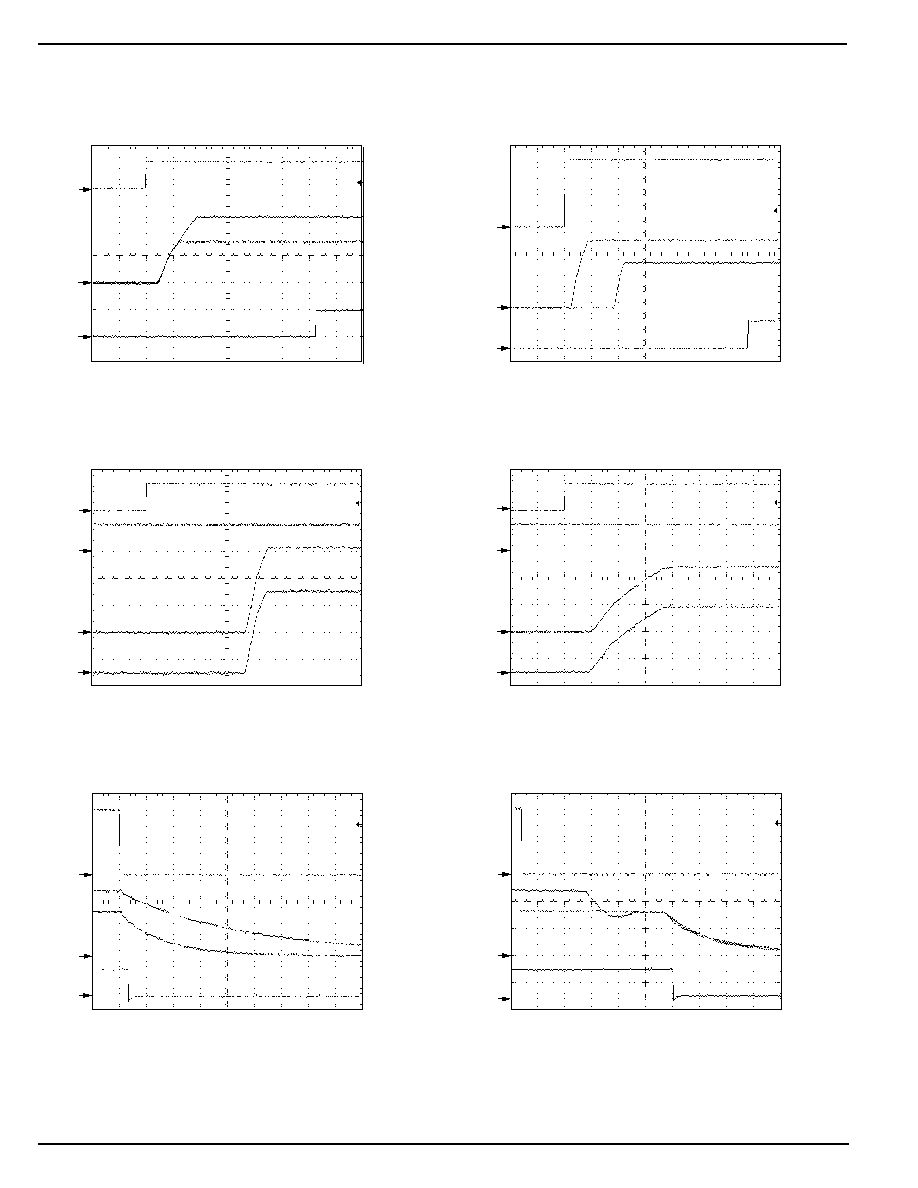
Functional Characteristics
Turn-On (No Delay)
TIME (5ms/div.)
ON
5V/div
V
OUT1
V
OUT2
2V/div
/POR
5V/div
V
CC1
= 5V
V
CC2
= 3.3V
R
L1
= 3.5
R
L2
= 1
C
L1
= C
L2
= 220
µ
F
Turn-On, Staggered Mode
(MIC2585-1BTS)
TIME (10ms/div.)
ON
2V/div
V
OUT1
V
OUT2
2V/div
/POR
5V/div
V
CC1
= 5V
V
CC2
= 3.3V
C
DLY
= 47nF
R
L1
= R
L2
= OPEN
ON
5V/div
/F
A
U
L
T
5V/div
V
OUT2
1V/div
I
IN2
1A/div
V
CC1 =
5V
V
CC2 =
3.3V
R
L2
=1
C
L2
= 220
µ
F
Turn-On (Channel 2)
TIME (5ms/div.)
ON
5V/div
/F
A
U
L
T
5V/div
V
OUT1
2V/div
I
IN1
2A/div
V
CC1 =
5V
V
CC2 =
3.3V
R
L1
=1
C
L1
= 220
µ
F
Turn-On (Channel 1)
TIME (2.5ms/div.)
ON
2V/div
V
OUT1
V
OUT2
2V/div
/POR
5V/div
Turn-Off (Tracking On)
TIME (1ms/div.)
V
CC1 =
5V
V
CC2 =
3.3V
R
L1
= 1
R
L2
= 3
C
L1
= 2200
µ
F
C
L2
= 220
µ
F
ON
2V/div
V
OUT1
V
OUT2
2V/div
/POR
5V/div
V
CC1 =
5V
V
CC2 =
3.3V
R
L1
= 1
R
L2
= 3
C
L1
= 2200
µ
F
C
L2
= 220
µ
F
Turn-Off (Tracking Off)
TIME (500
µ
s/div.)
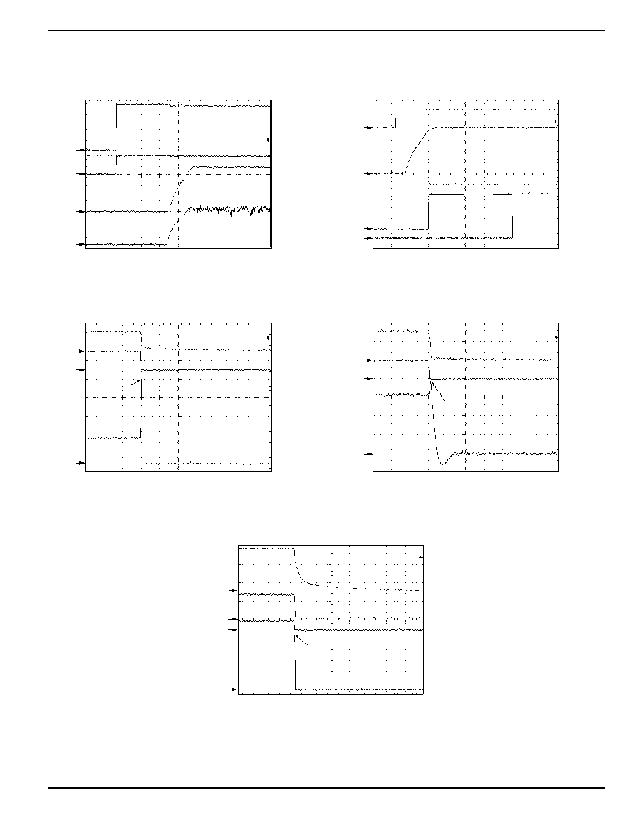
March 2005
13
MIC2584/2585
MIC2584/2585
Micrel
Turn-On Response (Hot Insert)
TIME (5ms/div.)
VCC1
2V/div
FA
U
L
T
5V/div
V
OUT1
2V/div
I
IN1
500mA/div
V
CC1
= 5V
V
CC2
= 3.3V
C
L
= 250
µ
F
R
L
= 5
ON
5V/div
V
OUT1
2V/div
PG1
2V/div
/POR
2V/div
22.5ms
Power-On Reset Response
TIME (5ms/div.)
V
CC1 =
5V
V
CC2 =
3.3V
R
L1
=3.5
C
L1
= 220
µ
F
C
POR
= 47nF
FA
U
L
T
5V/div
V
OUT1
5V/div
I
IN1
1A/div
Short-Circuit Crowbar Channel 1
(SCR enabled through a PNP from DIS pin-MIC2585-1BTS)
TIME (25
µ
s/div.)
V
CC1
=
5V
V
CC2
=
3.3V
R
L1
= 3.5
R
L2
= 1
C
L1
= C
L2
= 220
µ
F
4.5A peak
/F
A
U
L
T
5V/div
V
OUT2
2V/div
I
IN2
1A/div
Short-Circuit Crowbar Channel 2
(SCR enabled through a PNP from DIS pin-MIC2585-1BTS)
TIME (10
µ
s/div.)
V
CC1
=
5V
V
CC2
=
3.3V
R
L1
= 3.5
R
L2
= 1
C
L1
= C
L2
= 220
µ
F
3.88A peak
V
OUT1
2V/div
V
GA
TE1
10V/div
FA
U
L
T
10V/div
I
IN1
2A/div
6.04A peak
V
CC1 =
5V
V
CC2 =
3.3V
R
L1
= 1
R
L2
= open
C
L1
= 2200
µ
F
C
L2
= 220
µ
F
Short-Circuit Response
TIME (25
µ
s/div.)
MIC2584/2585
Micrel
MIC2584/2585
14
March 2005
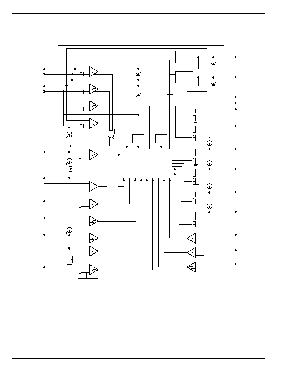
Functional Diagram
V
REF
V
REF
0.8V
V
REF
I
CPOR
V
CC1
V
CC1
I
TMR
0.3V
0.3V
0.8V
V
REF
V
REF
V
REF
Glitch
Filter
100mV
2.5
µ
A
2.5
µ
A
100mV
50mV
+
50mV
MIC2585-J
UVLO2
0.8V
UVLO1
2.165V
Up & Down
Tracking
Charge
Pump
2
Charge
Pump
1
GATE1
GATE2
21V
OUT1
OUT2
DIS1
DIS2
/FAULT
/POR
PG1
PG2
TRK
OV1
OV2
4
21
9
16
17
15 (11)
14 (10)
6
19
5 (4)
20 (13)
3 (3)
22 (14)
SENSE1
23 (15)
VCC1
24 (16)
SENSE2
2 (2)
VCC2
1 (1)
CFILTER
11 (8)
GND
13 (9)
FB1
18 (12)
FB2
7 (5)
CDLY
12
CPOR
10 (7)
ON
8 (6)
Glitch
Filter
1.235V
Reference
Logic
+
≠
+
≠
+
≠
+
≠
+
≠
+
≠
+
≠
+
≠
+
≠
+
≠
+
≠
+
≠
+
≠
+
≠
2.5
µ
A
Pin numbers for MIC2584 are in parenthesis ( ) where applicable
V
CC1
20
µ
A
V
CC1
20
µ
A
V
CC1
20
µ
A
V
CC1
20
µ
A
21V
10V
10V

March 2005
15
MIC2584/2585
MIC2584/2585
Micrel
Functional Description
Hot Swap Insertion
When circuit boards are inserted into live system backplanes
and supply voltages, high inrush currents can result due to
the charging of bulk capacitance that resides across the
supply pins of the circuit board. This inrush current, although
transient in nature, may be high enough to cause permanent
damage to on-board components or may cause the system's
supply voltages to go out of regulation during the transient
period which may result in system failures. The MIC2584 and
MIC2585 act as a controller for external N-Channel MOSFET
devices in which the gate drive is controlled to provide inrush
current limiting and output voltage slew rate control during hot
swap insertions.
Power Supply
VCC1 is the main supply input to the MIC2584/85 controller
with a voltage range of 2.3V to 13.2V. The VCC2 supply input
ranges from 1.0V to 13.2V and must be less than or equal to
VCC1 for operation. Both inputs can withstand transient
spikes up to 20V. In order to ensure stability of the supplies,
a minimum 1
µ
F capacitor from each VCC to ground is
recommended. Alternatively, a low pass filter, shown in the
typical application circuit, can be used to eliminate high
frequency oscillations as well as help suppress transient
spikes.
Also, due to the existence of undetermined parasitic induc-
tance in the absence of bulk capacitance, placing a Zener
diode at each VCC of the controller to ground in order to
provide external supply transient protection is strongly rec-
ommended. See the typical application circuit in Figure 1.
Start-Up Cycle
Supply Contact Delay
During a hot insert of a PC board into a backplane or when the
main supply (VCC1) is powered up from a cold start, as the
voltage at the ON pin rises above its threshold (1.235V
typical), the MIC2584/85 first checks that both supply volt-
ages are above their respective UVLO thresholds. If so, then
the device is enabled and an internal 2.5
µ
A current source
begins charging capacitor C
POR
to 0.3V to initiate a start-up
sequence. Once the start-up delay (t
START
) elapses, the
CPOR pin is pulled immediately to ground and a separate
14
µ
A current source begins charging each GATE output to
drive the external MOSFET that switches V
IN
to V
OUT
. The
programmed contact start-up delay is calculated using the
following equation:
t
C
V
I
0.12 C
( F)
START
POR
START
CPOR
POR
=
◊
◊
µ
(1)
where the start-up delay timer threshold (V
START
) is 0.3V,
and the Power-On Reset timer current (I
CPOR
) is 2.5
µ
A. See
Table 2 for some typical supply contact start-up delays using
several standard value capacitors. As each GATE voltage
continues ramping toward its final value (V
CC
+ V
GS
) at a
defined slew rate (See Load Capacitance/Gate Capacitance
Dominated Start-Up sections), a second CPOR timing cycle
begins if: 1)/FAULT is high and 2)CFILTER is low (i.e., not an
overvoltage, undervoltage lockout, or overcurrent state).
This second timing cycle (t
POR
) begins when the lagging
voltage exceeds its FB pin threshold (V
FB
). See Figure 4 in
the "
Timing Diagrams
". When the power supply is already
present (i.e., not a "hot swapping" condition) and the MIC2584/
85 device is enabled by applying a logic high signal at the ON
pin, the GATE outputs begin ramping immediately as the first
CPOR timing cycle is bypassed. Active current regulation is
employed to limit the inrush current transient response during
start-up by regulating the load current at the programmed
current limit value (See "
Current Limiting and Dual-Level
Circuit Breaker
" section). The following equation is used to
determine the nominal current limit value:
I
V
R
50mV
R
LIM
TRIPSLOW
SENSE
SENSE
=
=
(2)
where V
TRIPSLOW
is the current limit slow trip threshold found
in the electrical table and R
SENSE
is the selected value that
will set the desired current limit. There are two basic start-up
modes for the MIC2584/85: 1)Start-up dominated by load
capacitance and 2)start-up dominated by total gate capaci-
tance. The magnitude of the inrush current delivered to the
load will determine the dominant mode. If the inrush current
is greater than the programmed current limit (I
LIM
), then load
capacitance is dominant. Otherwise, gate capacitance is
dominant. The expected inrush current may be calculated
using the following equation:
INRUSH
I
C
C
14 A
C
C
GATE
LOAD
GATE
LOAD
GATE
◊
µ ◊
(3)
where I
GATE
is the GATE pin pull-up current, C
LOAD
is the
load capacitance, and C
GATE
is the total GATE capacitance
(C
ISS
of the external MOSFET and any external capacitor
connected from the MIC2584/85 GATE pin to ground).
Load Capacitance Dominated Start-Up
In this case, the load capacitance (C
LOAD
) is large enough to
cause the inrush current to exceed the programmed current
limit but is less than the fast-trip threshold (or the fast-trip
threshold is disabled, `M' option). During start-up under this
condition, the load current is regulated at the programmed
current limit value (I
LIM
) and held constant until the output
voltage rises to its final value. The output slew rate and
equivalent GATE voltage slew rate is computed by the
following equation:
Output Voltage Slew Rate dV
/dt
I
C
OUT
LIM
LOAD
,
=
(4)
where I
LIM
is the programmed current limit value. Conse-
quently, the value of C
FILTER
must be selected to ensure that
the overcurrent response time, t
OCSLOW
, exceeds the time
needed for the output to reach its final value. For example,
given a MOSFET with an input capacitance C
ISS
= C
GATE
=
2000pF, C
LOAD
is 1000
µ
F, and I
LIM
is set to 5A with a 12V
input, then the load capacitance dominates as determined by
the calculated INRUSH > I
LIM
. Therefore, the output voltage
slew rate determined from Equation 4 is:
Output Voltage Slew Rate, (dV
/dt)
5A
100 F
V
ms
OUT
=
µ
=
5

MIC2584/2585
Micrel
MIC2584/2585
16
March 2005
and the resulting t
OCSLOW
needed to achieve a 12V output is
approximately 2.5ms. (See "
Power-On Reset, Overcurrent
Timer, and Sequenced Output Delays
" section to calculate
t
OCSLOW
).
GATE Capacitance Dominated Start-Up
In this case, the value of the load capacitance relative to the
GATE capacitance is small enough such that during start-up
the output current never exceeds the current limit threshold
as determined by Equation 3. The minimum value of C
GATE
that will ensure that the current limit is never exceeded is
given by the equation below:
C
(Min)
I
I
C
GATE
GATE
LIMIT
LOAD
=
◊
Where C
GATE
is the summation of the MOSFET input capaci-
tance (C
ISS
) specification and the value of the capacitor
connected to the GATE pin of the MIC2584/85 (and MOSFET)
to ground. Once C
GATE
is determined, use the following
equation to determine the output slew rate
dV
OUT
/dt for gate capacitance dominated start-up:
dV
/dt
I
C
OUT
GATE
GATE
=
Table 1 depicts the output slew rate for various values of C
GATE
.
I
GATE
= 14
µ
A
C
GATE
dV
OUT
/dt
0.001
µ
F
14V/ms
0.01
µ
F
1.4V/ms
0.1
µ
F
0.14V/ms
1
µ
F
0.014V/ms
Table 1. Output Slew Rate Selection for GATE
Capacitance Dominated Start-Up
Current Limiting and Dual-Level Circuit Breaker
Many applications will require that the inrush and steady state
supply current be limited at a specific value in order to protect
critical components within the system. Connecting a sense
resistor between the VCC and SENSE pins of each channel
sets the nominal current limit value for each channel of the
MIC2584/85 and the current limit is calculated using
Equation 2.
The MIC2584/85 also features a dual-level circuit breaker
triggered via 50mV and 100mV current limit thresholds sensed
across the VCC and SENSE pins. The first level of the circuit
breaker functions as follows. For the MIC2584/85, once the
voltage sensed across these two pins exceeds 50mV on
either channel, the overcurrent timer, its duration set by
capacitor C
FILTER
, starts to ramp the voltage at CFILTER
using a 2.5
µ
A constant current source. If the voltage at
CFILTER reaches the overcurrent timer threshold (V
TMR
) of
1.235V, then CFILTER immediately returns to ground as the
circuit breaker trips and both GATE outputs are immediately
shut down. For the second level, if the voltage sensed across
VCC and SENSE of either channel exceeds 100mV
(≠J option) at any time, the circuit breaker trips and both
GATE outputs shut down immediately, bypassing the
overcurrent timer period. To disable current limit and circuit
breaker operation, tie each channel's SENSE and VCC pins
together and the CFILTER pin to ground.
Output Undervoltage Detection
The MIC2584/85 employ output undervoltage detection by
monitoring the output voltage through a resistive divider
connected at the FB pins. During turn on, while the voltage at
either FB pin is below its threshold (V
FB
), the /POR pin is
asserted low. Once both FB pin voltages cross their respec-
tive threshold (V
FB
), a 2.5
µ
A current source charges capaci-
tor C
POR
. Once the CPOR pin voltage reaches 1.235V, the
time period t
POR
elapses as pin CPOR is pulled to ground and
the /POR pin goes HIGH. If the voltage at either FB drops
below V
FB
for more than 10
µ
s, the /POR pin resets for at least
one timing cycle defined by t
POR
(See "
Applications Informa-
tion
" for an example).
Input/Output Overvoltage Protection
The MIC2585 monitors and detects overvoltage conditions in
the event of excessive supply transients at the MIC2585
input(s)/output(s). Whenever the voltage threshold is ex-
ceeded at either OV1 or OV2 of the MIC2585, the circuit
breaker is tripped and both GATE outputs are immediately
brought low.
Power-On Reset, Overcurrent Timer, and Sequenced
Output Delays
The Power-On Reset delay, t
POR
, is the time period for the
/POR pin to go HIGH once the lagging voltage exceeds the
power-good threshold (V
FB
) monitored at the FB pin. A
capacitor connected to CPOR sets the interval and is deter-
mined by using Equation 1 with V
POR
substituted for V
START
.
The resulting equation becomes:
t
C
V
I
0.5 C
F
POR
POR
POR
CPOR
POR
=
◊
◊
µ
( )
(7)
where the Power-On Reset threshold (V
POR
) and timer
current (I
CPOR
) are typically 1.235V and 2.5
µ
A, respectively.
For the MIC2584/85, a capacitor connected to CFILTER is
used to set the timer which activates the circuit breaker during
overcurrent conditions. When the voltage across either sense
resistor exceeds the slow trip current limit threshold of 50mV,
the overcurrent timer begins to charge for a period, t
OCSLOW
,
determined by C
FILTER
. If t
OCSLOW
elapses, then the circuit
breaker is activated and both GATE outputs are immediately
pulled to ground. The following equation is used to determine
the overcurrent timer period, t
OCSLOW
.
t
C
V
I
0.5 C
( F)
OCSLOW
FILTER
TMR
TMR
FILTER
=
◊
◊
µ
(8)
where V
TMR
, the overcurrent timer threshold, is 1.235V and
I
TMR
, the overcurrent timer current, is 2.5
µ
A. If no capacitor
for CFILTER is used, then t
OCSLOW
defaults to 20
µ
s.
March 2005
17
MIC2584/2585
MIC2584/2585
Micrel
The sequenced output feature is enabled for the MIC2585 by
placing a capacitor from CDLY to ground. The ≠1 option
allows for V
OUT2
to follow V
OUT1
and the ≠2 option allows for
V
OUT1
to follow V
OUT2
during start-up (See "
Timing Dia-
grams, Figure 5
"). The sequenced output delay time is
determined using the following equation:
t
C
V
I
0.2 C
( F)
DLY
DLY
DELAY
DELAY
DLY
◊
◊
µ
(9)
where V
DELAY
, the CDLY pin threshold, is typically 1.235V,
I
DELAY
, the CDLY pin charge current, is typically 6
µ
A, and
C
DLY
is the capacitor connected to CDLY. Tables 2, 3, and 4
provide a quick reference for several timer calculations using
select standard value capacitors.
Undervoltage Lockout
Internal circuitry keeps both GATE output charge pumps off
until VCC1 and VCC2 exceed 2.165V and 0.8V, respectively.
C
POR
t
START
t
POR
0.01
µ
F
1.2ms
5ms
0.033
µ
F
4ms
16.5ms
0.05
µ
F
6ms
25ms
0.1
µ
F
12ms
50ms
0.33
µ
F
40ms
165ms
0.47
µ
F
56ms
235ms
1
µ
F
120ms
500ms
Table 2. Selected Power-On Reset and
Start-Up Delays
C
FILTER
t
OCSLOW
220pF
110
µ
s
680pF
340
µ
s
1000pF
500
µ
s
3300pF
1.6ms
0.01
µ
F
5ms
0.047
µ
F
23.5ms
0.1
µ
F
50ms
0.33
µ
F
165ms
Table 3. Selected Overcurrent Timer Delays
C
DLY
t
DLY
4700pF
950
µ
s
0.01
µ
F
2ms
0.047
µ
F
9.5ms
0.1
µ
F
20ms
0.33
µ
F
66ms
0.82
µ
F
165ms
1
µ
F
200ms
2.2
µ
F
440ms
Table 4. Selected Sequenced Output Delays

MIC2584/2585
Micrel
MIC2584/2585
18
March 2005
C6
0.1
µ
F
R1
47k
SENSE1
VCC1
R
SENSE1
0.007
5%
1
3
4
24
23
SENSE2
VCC2
R
SENSE2
0.015
5%
1
2
3
4
1
2
C4
0.022
µ
F
**Q2
Si4922DY (1)
(SO-8)
C
LOAD1
1500
µ
F
V
OUT1
5V@5A
V
OUT2
1.8V@2A
C
LOAD2
100
µ
F
C3
0.022
µ
F
**Q1
Si4922DY (2)
(SO-8)
GND
3
5
9
7
22
20
18
13
GATE2
OUT2
TRK
OUT1
FB2
FB1
GATE1
CDLY
12
CFILTER
11
ON
8
Undervoltage (OUT1) = 4.4V
Undervoltage (OUT2) = 1.5V
Circuit Breaker Response Time = 5ms
Sequenced Output Delay = 20ms
*Diodes are BZX84C(x)V(x)
**Si4922DY is a dual Power MOSFET
Additional pins omitted for clarity
C5
0.01
µ
F
C2
1
µ
F
R5
10.5k
1%
R3
15.8k
1%
R2
39.2k
1%
R4
8.06k
1%
*D1
(8V)
*D2
(6V)
C1
1
µ
F
MIC2585-1
V
IN1
5V
V
IN2
1.8V
Figure 6. Output Sequencing/Tracking Combination
Applications Information
Output Tracking and Sequencing
The MIC2585 is equipped with optional supply
settings: Tracking or Sequencing. There are many applica-
tions that require two supplies to track one another within a
specified maximum potential difference (or time) during power-
up and power-down, such as in switching a processor on and
off. In many other systems and applications, supply sequenc-
ing during turn-on may be essential such as when a specific
circuit block (e.g., a system clock) requires available power
before another block of system circuitry. For either supply
configuration, the MIC2585 requires only one additional
component and can be used as an integrated solution to
traditional, and most often complex, discrete circuit solutions.
Additionally, the two optional supply settings may be com-
bined to provide supply sequencing during start-up and
supply tracking during turn-off (see Figure 6 below). The
MIC2585 guarantees supply tracking within 250mV for power-
up and power-down independent of the load capacitance of
each supply. See "
Figure 2
" of the "
Timing Diagrams
".
Wiring the TRK pin to either OUT1 or OUT2 of the MIC2585
enables the tracking feature. The OUT1 and OUT2 pins
provide output track sensing and are wired directly to the
output (source) of the external MOSFET for Channel 1 and
Channel 2, respectively.
The MIC2584/85 can also be used in systems that support
more than two supplies. Figure 7 illustrates the generic use
of two separate controllers configured to support four inde-
pendent supply rails with an associated output timing re-
sponse. The PG (or /POR) output of the first controller is used
to enable the second controller. As configured, a fault condi-
tion on either V
OUT1
or V
OUT2
will result in all channels being
shut down. For systems with multiple power sequencing
requirements, the controllers' output tracking and sequenc-
ing features can be implemented in order to meet the system's
timing demands.
March 2005
19
MIC2584/2585
MIC2584/2585
Micrel
Fast Output Discharge for Capacitive Loads
In many applications where a switch controller is turned off by
either removing the PCB from the backplane or the ON pin is
reset, capacitive loading will cause the output to retain
voltage unless a `bleed' (low impedance) path is in place in
order to discharge the capacitance. The MIC2585 is equipped
with an internal MOSFET that allows the discharging of any
load capacitance to ground through a 50
to 170
path. The
discharge feature is configured by wiring the DIS pin to the
output (source) of the external MOSFET and is enabled if the
TRK pin is below 0.3V after the controller has been disabled
by a logic low signal received at the ON pin of Figure 1. See
the "
Typical Application
" circuit of Figure 1. A series resistor
is required from DIS to V
OUT
so that the maximum current of
25mA for the DIS pin is not exceeded.
Output Turn-Off Sequencing - No Tracking
There are many applications where it is necessary or desir-
able for the supply rails to sequence during turn-on and turn-
off, as is the case with some microprocessor requirements.
The MIC2585 can be configured to allow one output to shut
off first, followed by the other output. Figure 8 illustrates an
example circuit that sequences OUT1 and OUT2 in a first on≠
last off application. During start-up, capacitor C
DLY
allows for
V
OUT1
to turn on followed by V
OUT2
20ms later. Once the ON
pin receives a low signal by removing the PCB from the
backplane, or by an external processor signal, DIS1 and DIS2
will assert low. The external crowbar circuit connected from
the DIS2 pin will immediately bring V
OUT2
to ground while
V
OUT1
will discharge to ground through the 750
(680
external, 70
internal) series path.
MIC2585
ON
/FAULT
PG
GATE1
OUT1
GATE2
OUT2
V
OUT1
V
IN1
V
IN2
V
IN3
V
IN4
EN
V
OUT2
MIC2585
ON
/FAULT
GATE1
OUT1
GATE2
OUT2
V
OUT3
V
OUT4
V
OUT1
/V
OUT2
Short Circuit
on V
OUT1
System Timing
V
OUT3
/V
OUT4
ON
PG
/FAULT
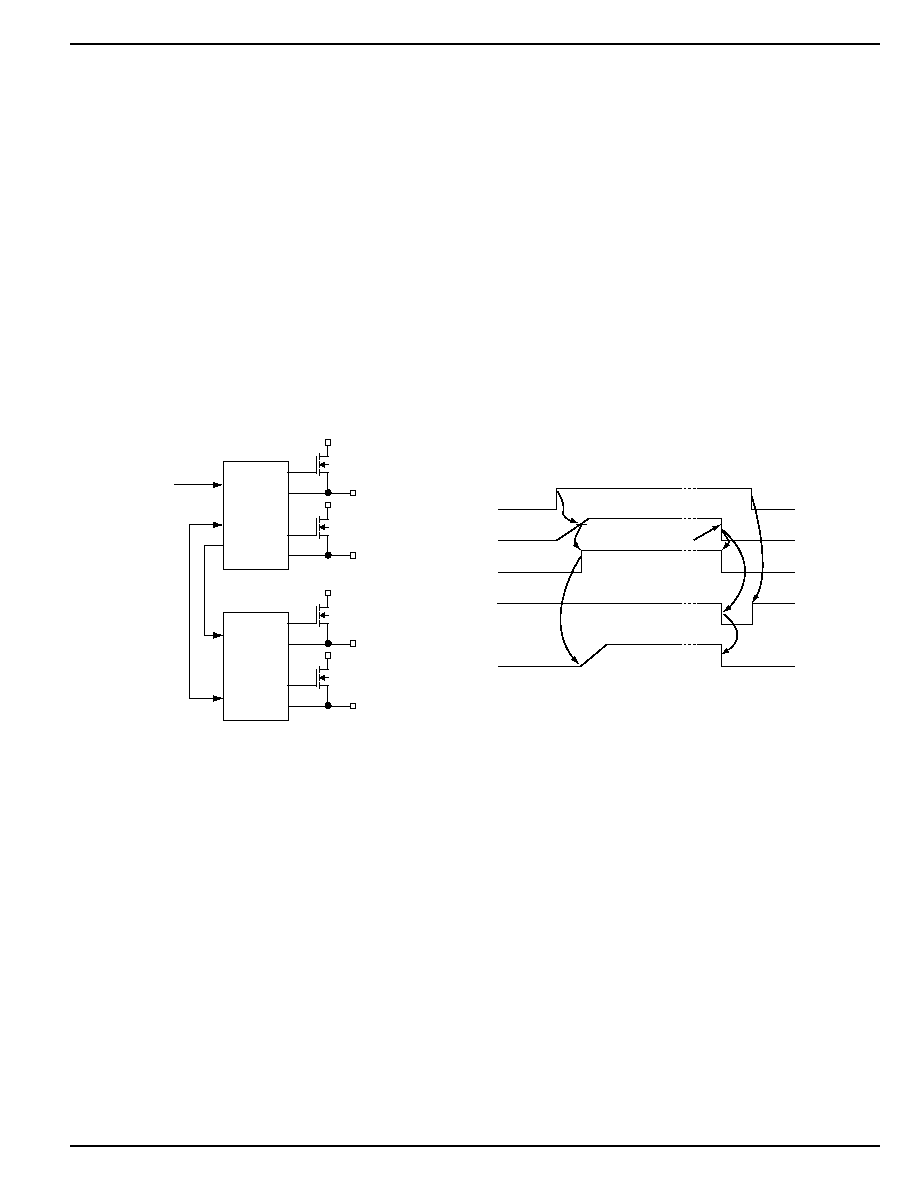
Figure 7. Supporting More Than Two Supplies
MIC2584/2585
Micrel
MIC2584/2585
20
March 2005
2) Next, determine R12 using the output "good"
voltage of 10.5V and the following equation:
V
V
R12 R13
R13
OUT1(Good)
FB1(MAX)
=
+
(
)
(10)
Using some basic algebra and simplifying Equation 10 to
isolate R12, yields:
R12
R13
V
V
≠ 1
OUT1(Good)
FB1(MAX)
=
(10.1)
where V
FB1(MAX)
= 1.29V, V
OUT1(Good)
= 10.5V, and R13 is
14.7k
. Substituting these values into Equation 10.1 now
yields R12 = 104.95k
. A standard 105k
±
1% is selected.
Now, consider the 11.4V minimum output voltage, the lower
tolerance for R13 and higher tolerance for R12, 14.55k
and
106.05k
, respectively. With only 11.4V available, the voltage
sensed at the FB1 pin exceeds V
FB1(MAX)
, thus the /POR and
PG1 (MIC2585) signals will transition from LOW to HIGH,
indicating "power is good" given the worse case tolerances of
this example. A similar approach should be used for Channel 2.
Output Undervoltage Detection
For output undervoltage detection, the first consideration is to
establish the output voltage level that indicates "power is
good." For this example, the output value for which a 12V
supply will signal "good" is 10.5V. Next, consider the toler-
ances of the input supply and FB threshold (V
FB
). For this
example, given a 12V
±
5% supply for Channel 1, the resulting
output voltage may be as low as 11.4V and as high as 12.6V.
Additionally, the FB1 threshold has
±
50mV tolerance and
may be as low as 1.19V and as high as 1.29V. Thus, to
determine the values of the resistive divider network (R12
and R13) at the FB1 pin, shown in the typical application
circuit on page 1, use the following iterative design proce-
dure.
1) Choose R13 so as to limit the current through
the divider to approximately 100
µ
A or less.
R13
V
100 A
1.29V
100 A
12.9k
FB1(MAX)
µ
µ
.
R13 is chosen as 14.7k
±
1%.
C6
0.1
µ
F
R1
33k
R2
47k
SENSE1
VCC1
R
SENSE1
0.012
5%
1
2
3
4
24
23
SENSE2
VCC2
R
SENSE2
0.012
5%
1
2
3
4
1
2
C4
0.022
µ
F
Q2
IRF7822
(SO-8)
C
LOAD1
220
µ
F
V
OUT1
5V@2.5A
V
OUT2
3.3V@2.5A
C
LOAD2
220
µ
F
C3
0.022
µ
F
C7
0.033
µ
F
Q4
TCR22-4
Q3
ZTX788A
Q1
IRF7822
(SO-8)
GND
TRK
3
5
6
7
22
20
18
13
9
GATE2
OUT2
DIS2
19
DIS1
OUT1
FB2
FB1
GATE1
CDLY
12
CFILTER
11
ON
8
Undervoltage (OUT1) = 4.4V
Undervoltage (OUT2) = 2.85V
Circuit Breaker Response Time = 5ms
Sequenced Output Delay (Turn-On) = 20ms
*Dual package Diode is AZ23C8V2
Resistors are 5% unless specified otherwise
Additional pins omitted for clarity
C5
0.01
µ
F
C2
1
µ
F
R6
8.66k
1%
R7
680
R8
1.5k
R10
360
R9
3.6k
R3
39.2k
1%
R4
15.8k
1%
R5
20.5k
1%
*D1
(8V)
*D2
(8V)
C1
1
µ
F
MIC2585-1
V
IN1
5V
V
IN2
3.3V
Figure 8. First On--Last Off Application Circuit

March 2005
21
MIC2584/2585
MIC2584/2585
Micrel
Input Overvoltage Protection
A similar design approach as the previous Undervoltage
Detection example is recommended for the overvoltage
protection circuitry, resistors R6 and R7 for OV1, in Figure 1.
For input overvoltage protection, the first consideration is to
establish the input voltage level that indicates an overvoltage
triggering a system (output voltage) shut down. For our
example, the input value for which the Channel 1 12V supply
will signal an "output shutdown" is 13.2V (+10%). Similarly,
from the previous example:
1) Choose R7 to satisfy 100
µ
A condition.
R7
V
100 A
1.19V
100 A
11.9k
OV1(MIN)
µ
µ
R7 is chosen as 13.0k
±
1%
2) Thus, following the previous example and
substituting R6 and R7 for R12 and R13,
respectively, V
OV1(MIN)
for V
FB1(MAX)
, and 13.2V
overvoltage for 10.5V output "good," the same
formula yields R6 of 131.2k
. The nearest
standard 1% value is 130k
.
Now, consider the 12.6V maximum input voltage
(V
CC1
+5%), the higher tolerance for R7 and lower tolerance
for R6, 13.13k
and 128.7k
, respectively. With 12.6V input,
the voltage sensed at the OV1 pin is below V
OV1(MIN)
, and the
MIC2584/85 will not indicate an overvoltage condition until
V
CC1
exceeds approximately 13.2V considering the given
tolerances. A similar approach should be used for Channel 2.
PCB Connection Sense
There are several configuration options for the MIC2584/85's
ON pin to detect if the PCB has been fully seated in the
backplane before initiating a start-up cycle. In Figure 1, the
MIC2584/85 is mounted on the PCB with a resistive divider
network connected to the ON pin. R4 is connected to a short
pin on the PCB edge connector. Until the connectors mate,
the ON pin is held low which keeps the GATE output charge
pump off. Once the connectors mate, the resistor network is
pulled up to the input supply, 12V in this example, and the ON
pin voltage exceeds its threshold (V
ON
) of 1.235V and the
MIC2584/85 initiates a start-up cycle. In Figure 9, the connec-
tion sense consisting of a discrete logic-level MOSFET
and a few resistors allows for interrupt control from the
processor or other signal controller to shut off the output of the
MIC2584/85. R4 pulls the GATE of Q2 to V
IN
and the ON pin
is held low until the connectors are fully mated. Once the
connectors fully mate, a logic LOW at the /ON_OFF signal
turns Q2 off and allows the ON pin to pull up above its
threshold and initiate a start-up cycle. Applying a logic HIGH
at the /ON_OFF signal will turn Q2 on and short the ON pin
of the MIC2584/85 to ground which turns off the GATE output
charge pump.
GND
/ON_OFF
C3
0.033
µ
F
C4
0.01
µ
F
SENSE1
VCC1
ON
CPOR
OUT1
FB1
GATE1
GND
/POR
CFILTER
/FAULT
Long
Pin
Backplane
Connector
PCB Edge
Connector
Long
Pin
Medium or
Short Pin
Undervoltage (Output) = 4.45V
/POR Delay = 16.5ms
START-UP Delay = 4ms
Circuit Breaker Response Time = 5ms
*Q2 is TN0201T (SOT-23)
Channel 2 and additional pins omitted for clarity.
Downstream
Signal
Short
Pin
PCB Connection Sense
Q1
Si7892DP
(PowerPAKTM SO-8)
R5
10
R7
10.5k
1%
R4
20k
R1
33k
R3
33
*Q2
MIC2584
C1
1
µ
F
C2
0.01
µ
F
C
LOAD1
1000
µ
F
R2
33k
R6
27.4k
1%
V
OUT1
5V@7A
V
IN1
5V
/FAULT
11
9
7
8
16
15
12
13
6
10
14
R
SENSE1
0.005
5%
1
2
3
4
Figure 9. PCB Connection Sense with ON/OFF Control

MIC2584/2585
Micrel
MIC2584/2585
22
March 2005
Higher UVLO Setting
Once a PCB is inserted into a backplane (power supply), the
internal UVLO circuit of the MIC2584/85 holds the GATE
output charge pump off until VCC1 exceeds 2.165V and
VCC2 exceeds 0.8V. If VCC1 falls below 1.935V or VCC2
falls below 0.77V, the UVLO circuit pulls the GATE output to
ground and clears the overvoltage and/or current limit faults.
For a higher UVLO threshold, the circuit in Figure 10 can be
used to delay the output MOSFET from switching on until the
desired input voltage is achieved. The circuit allows the
charge pumps to remain off until V
IN1
exceeds
1
R1
R2
1.235V
+
◊
provided that VCC2 has exceeded its
threshold. Both GATE drive outputs will be shut down when
V
IN1
falls below 1
R1
R2
1.21V
+
◊
. In the example circuit , the
rising UVLO threshold is set at approximately 9.0V and the
falling UVLO threshold is established as 8.9V. The circuit
consists of an external resistor divider at the ON pin that
keeps both GATE output charge pumps off until the voltage
at the ON pin exceeds its threshold (V
ON
) and after the start-
up timer elapses.
Hot Swap Power Control for DSPs
In designing power supplies for dual supply logic devices,
such as a DSP, consideration should be given to the system
timing requirements of the core and I/O voltages for power-
up and power-down operations. When power is provided to
the core and I/O circuit blocks in an unpredictable manner,
the effects can be detrimental to the life cycle of the DSP or
logic device by allowing unexpected current to flow in the core
and I/O isolation structures. Additionally, bus contention is
one of the critical system-level issues supporting the need for
power supply sequencing. Since the core supplies logic
control for the bus, powering up the I/O before the core may
result in both the DSP and an attached peripheral device
being simultaneously configured as outputs. In this case, the
output drivers of each device contend for control over sending
data along the bus which may cause excessive current to flow
in one of the paths (I
1
or I
2
) shown in the bidirectional port of
Figure 11. Upon powering down the system, the core voltage
supply should turn off after the I/O as the bus control signal(s)
may enter an indeterminate state if the core is powered down
first. Thus, for power sequencing of a dual supply voltage
DSP implementing the MIC2585 (if V
CORE
V
I/O
), a circuit
similar to Figure 8 is recommended with the core voltage
supplied through Channel 1 and the I/O voltage supplied
through Channel 2. For systems with V
CORE
< V
I/O
, the
MIC2585-2 option with the I/O voltage through Channel 1 and
core through Channel 2 is used to implement the first on-last
off application.
Sense Resistor Selection
The MIC2584 and MIC2585 use a low-value sense resistor to
measure the current flowing through the MOSFET switch
(and therefore the load). This sense resistor is nominally set
at 50mV/I
LOAD(CONT)
. To accommodate worst-case toler-
ances for both the sense resistor (allow
±
3% over time and
temperature for a resistor with
±
1% initial tolerance) and still
supply the maximum required steady-state load current, a
slightly more detailed calculation must be used.
The current limit threshold voltage (i.e., the "trip point") for the
MIC2584/85 may be as low as 42.5mV, which would equate
to a sense resistor value of 42.5mV/I
LOAD(CONT)
. Carrying the
numbers through for the case where the value of the sense
resistor is 3% high yields:
R
42.5mV
1.03 I
41.3mV
I
SENSE(MAX)
LOAD(CONT)
LOAD(CONT)
=
(
)
(
)
=
(11)
Once the value of R
SENSE
has been chosen in this manner,
it is good practice to check the maximum I
LOAD(CONT)
which
the circuit may let through in the case of tolerance build-up in
SENSE1
VCC1
ON
FB1
GATE1
GND
Undervoltage Lockout Threshold (rising) = 9.0V
Undervoltage Lockout Threshold (falling) = 8.9V
Undervoltage (Output) = 11.4V
Channel 2 and additional pins omitted for clarity.
Q1
IRF7822
(SO-8)
R3
10
R5
16.2k
1%
R1
154k
1%
R2
24.3k
1%
MIC2584
C1
1
µ
F
D1
(18V)
C2
0.01
µ
F
C
LOAD1
1000
µ
F
R4
133k
1%
V
OUT1
12V@4A
V
IN1
12V
9
16
15
12
6
14
R
SENSE1
0.010
5%
1
2
3
4
Figure 10. Higher UVLO Setting

March 2005
23
MIC2584/2585
MIC2584/2585
Micrel
the opposite direction. Here, the worst-case maximum cur-
rent is found using a 57.5mV trip voltage and a sense resistor
that is 3% low in value. The resulting equation is:
I
57.5mV
0.97 R
59.3mV
R
LOAD(CONT,MAX)
SENSE(NOM)
SENSE(NOM)
=
(
)
(
)
=
(12)
As an example, if an output must carry a continuous 6A
without nuisance trips occurring, Equation 11
yields: R
41.3mV
6A
m
SENSE(MAX)
=
=
6 88
.
. The next lowest
standard value is 6m
. At the other set of tolerance extremes
for the output in question,
I
59.3mV
6.0m
A
LOAD(CONT,MAX)
=
=
9 88
.
. Knowing this final da-
tum, we can determine the necessary wattage of the sense
resistor using P = I
2
R, where I will be I
LOAD(CONT, MAX)
, and
R will be (0.97)(R
SENSE(NOM)
). These numbers yield the
following: P
MAX
= (9.88A)
2
(5.82m
) = 0.568W. In this ex-
ample, a 1W sense resistor is sufficient.
MOSFET Selection
Selecting the proper external MOSFET for use with the
MIC2584/85 involves three straightforward tasks:
∑ Choice of a MOSFET which meets minimum
voltage requirements.
∑ Selection of a device to handle the maximum
continuous current (steady-state thermal is-
sues).
∑ Verify the selected part's ability to withstand any
peak currents (transient thermal issues).
MOSFET Voltage Requirements
The first voltage requirement for the MOSFET is easily stated:
the drain-source breakdown voltage of the MOSFET must be
greater than V
IN(MAX)
. For instance, a 12V input may reason-
ably be expected to see high-frequency transients as high as
18V. Therefore, the drain-source breakdown voltage of the
MOSFET must be at least 19V. For ample safety margin and
standard availability, the closest minimum value will be 20V.
The second breakdown voltage criterion that must be met is a
bit subtler than simple drain-source breakdown voltage, but is
not hard to meet. In MIC2584/85 applications, the gate of the
external MOSFET is driven up to approximately 20V by the
internal output MOSFET (again, assuming 12V operation). At
the same time, if the output of the external MOSFET (its source)
is suddenly subjected to a short, the gate-source voltage will go
to (20V ≠ 0V) = 20V. This means that the external MOSFET
must be chosen to have a gate-source breakdown voltage of
20V or more, which is an available standard maximum value.
However, if operation is above 12V, the 20V gate-source
maximum will likely be exceeded. As a result, an external Zener
diode clamp should be used to prevent breakdown of the
external MOSFET when operating at voltages above 10V. A
Zener diode with 10V rating is recommended as shown in
Figure 12. At the present time, most power MOSFETs with a
20V gate-source voltage rating have a 30V drain-source break-
down rating or higher. As a general tip, choose surface-mount
devices with a drain-source rating of 30V as a starting point.
Finally, the external gate drive of the MIC2584/85 requires a
low-voltage logic level MOSFET when operating at voltages
lower than 3V. There are 2.5V logic level MOSFETs available.
See Table 5, "
MOSFET and Sense Resistor Vendors
" for
suggested manufacturers.
I
2
TX_/RX
I
1
V
DD
V
DD
CORE SUPPLY
(V
CC
)
OUTPUT
DRIVER
CIRCUIT
BLOCK
OUTPUT
DRIVER
CIRCUIT
BLOCK
Data In
OE
Data Out
External
Bus Control
I/O
Dual Supply DSP
Peripheral
CORE
I/O SUPPLY
(V
DD
)
Data In
OE
Data Out
Figure 11. Bidirectional Port Bus Contention
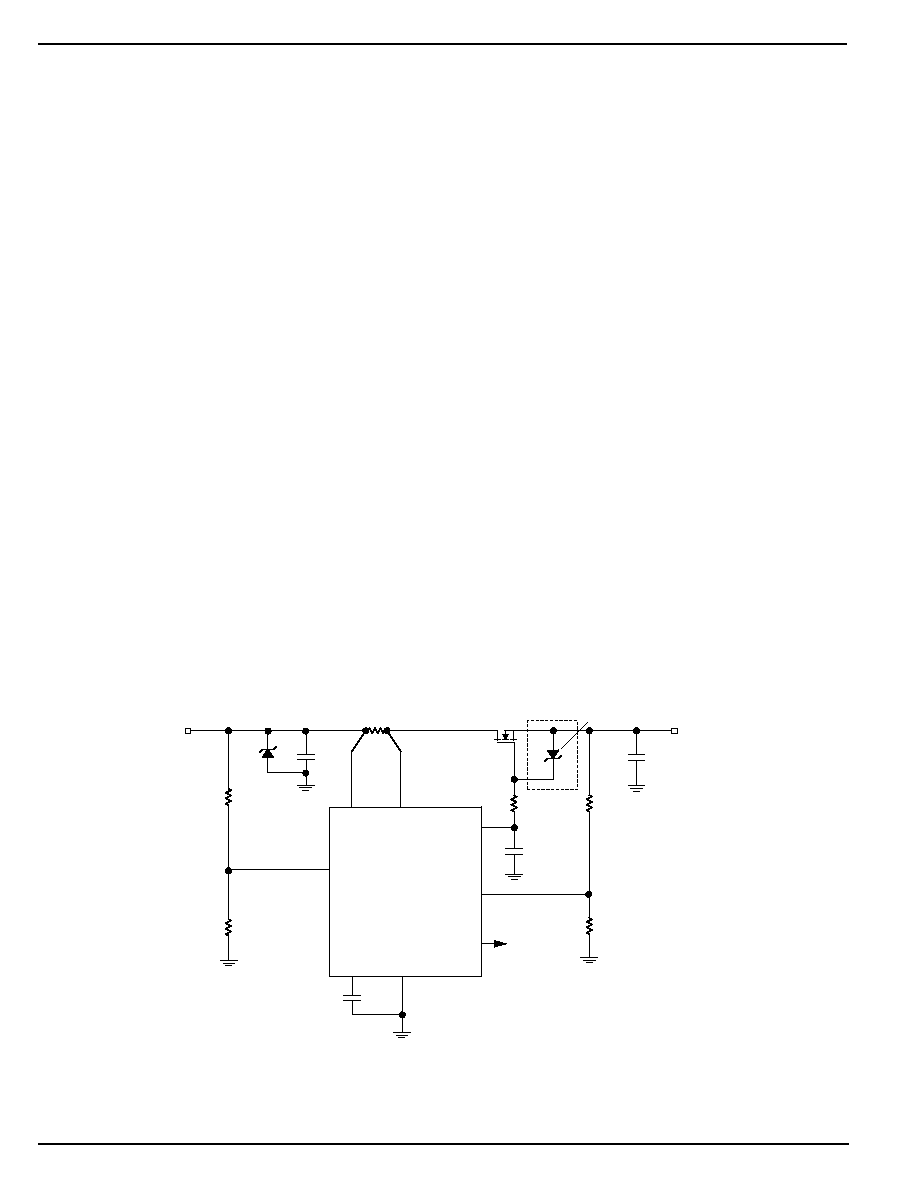
MIC2584/2585
Micrel
MIC2584/2585
24
March 2005
MOSFET Steady-State Thermal Issues
The selection of a MOSFET to meet the maximum continuous
current is a fairly straightforward exercise. First, arm yourself
with the following data:
∑ The value of I
LOAD(CONT, MAX.)
for the output in
question (see "
Sense Resistor Selection
").
∑ The manufacturer's data sheet for the candidate
MOSFET.
∑ The maximum ambient temperature in which the
device will be required to operate.
∑ Any knowledge you can get about the heat
sinking available to the device (e.g., can heat be
dissipated into the ground plane or power plane,
if using a surface-mount part? Is any airflow
available?).
The data sheet will almost always give a value of on resis-
tance given for the MOSFET at a gate-source voltage of 4.5V,
and another value at a gate-source voltage of 10V. As a first
approximation, add the two values together and divide by two
to get the on-resistance of the part with 8V of enhancement.
Call this value R
ON
. Since a heavily enhanced MOSFET acts
as an ohmic (resistive) device, almost all that's required to
determine steady-state power dissipation is to calculate I
2
R.
The one addendum to this is that MOSFETs have a slight
increase in R
ON
with increasing die temperature. A good
approximation for this value is 0.5% increase in R
ON
per
∞
C
rise in junction temperature above the point at which R
ON
was
initially specified by the manufacturer. For instance, if the
selected MOSFET has a calculated R
ON
of 10m
at a
T
J
= 25
∞
C, and the actual junction temperature ends up
at 110
∞
C, a good first cut at the operating value for R
ON
would be:
R
ON
10m
[1 + (110 - 25)(0.005)]
14.3m
The final step is to make sure that the heat sinking available
to the MOSFET is capable of dissipating at least as much
power (rated in
∞
C/W) as that with which the MOSFET's
performance was specified by the manufacturer. Here are a
few practical tips:
1. The heat from a surface-mount device such as
an SO-8 MOSFET flows almost entirely out of
the drain leads. If the drain leads can be sol-
dered down to one square inch or more, the
copper will act as the heat sink for the part. This
copper must be on the same layer of the board
as the MOSFET drain.
2. Airflow works. Even a few LFM (linear feet per
minute) of air will cool a MOSFET down sub-
stantially. If you can, position the MOSFET(s)
near the inlet of a power supply's fan, or the
outlet of a processor's cooling fan.
3. The best test of a surface-mount MOSFET for
an application (assuming the above tips show it
to be a likely fit) is an empirical one. Check the
MOSFET's temperature in the actual layout of
the expected final circuit, at full operating
current. The use of a thermocouple on the drain
leads, or infrared pyrometer on the package, will
then give a reasonable idea of the device's
junction temperature.
MOSFET Transient Thermal Issues
Having chosen a MOSFET that will withstand the imposed
voltage stresses, and the worse case continuous I
2
R power
dissipation which it will see, it remains only to verify the
MOSFET's ability to handle short-term overload power dissi-
pation without overheating. A MOSFET can handle a much
C3
0.05
µ
F
SENSE1
VCC1
ON
CPOR
FB1
GATE1
GND
/POR
Undervoltage (Output) = 11.0V
/POR Delay = 25ms
START-UP Delay = 6ms
*Recommended for MOSFETs with gate-source
breakdown of 20V or less for catastrophic output
short circuit protection. (IRF7822 VGS(MAX) = 12V)
Channel 2 and additional pins omitted for clarity.
Q1
IRF7822
(SO-8)
R3
10
*D2
1N5240B
10V
R5
13.3k
1%
R1
33k
R2
33k
MIC2584
C1
1
µ
F
C2
0.01
µ
F
C
LOAD1
220
µ
F
R4
100k
1%
V
OUT
12V@6A
V
IN
12V
11
9
7
16
15
12
6
14
R
SENSE1
0.006
5%
1
2
3
4
DOWNSTREAM
SIGNAL
D1
(18V)
Figure 12. Zener Clamped MOSFET Gate
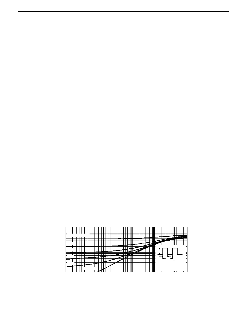
March 2005
25
MIC2584/2585
MIC2584/2585
Micrel
higher pulsed power without damage than its continuous
dissipation ratings would imply. The reason for this is that, like
everything else, thermal devices (silicon die, lead frames,
etc.) have thermal inertia.
In terms related directly to the specification and use of power
MOSFETs, this is known as "transient thermal impedance,"
or Z
(J-A)
. Almost all power MOSFET data sheets give a
Transient Thermal Impedance Curve. For example, take the
following case: V
IN
= 12V, t
OCSLOW
has been set to 100msec,
I
LOAD(CONT. MAX)
is 1.2A, the slow-trip threshold is 50mV
nominal, and the fast-trip threshold is 100mV. If the output is
accidentally connected to a 6
load, the output current from
the MOSFET will be regulated to 1.2A for 100ms (t
OCSLOW
)
before the part trips. During that time, the dissipation in the
MOSFET is given by:
P = E x I E
MOSFET
= [12V-(1.2A)(6
)] = 4.8V
P
MOSFET
= (4.8V x 1.2A) = 5.76W for 100msec.
At first glance, it would appear that a really hefty MOSFET is
required to withstand this sort of fault condition. This is where
the transient thermal impedance curves become very useful.
Figure 13 shows the curve for the Vishay (Siliconix) Si4410DY,
a commonly used SO-8 power MOSFET.
Taking the simplest case first, we'll assume that once a fault
event such as the one in question occurs, it will be a long time,
10 minutes or more, before the fault is isolated and the
channel is reset. In such a case, we can approximate this as
a "single pulse" event, that is to say, there's no significant duty
cycle. Then, reading up from the X-axis at the point where
"Square Wave Pulse Duration" is equal to 0.1sec (=100msec),
we see that the Z
(J-A)
of this MOSFET to a highly infrequent
event of this duration is only 8% of its continuous R
(J-A)
.
This particular part is specified as having an R
(J-A)
of
50
∞
C/W for intervals of 10 seconds or less. Thus:
Assume T
A
= 55
∞
C maximum, 1 square inch of copper at the
drain leads, no airflow.
Recalling from our previous approximation hint, the part has
an R
ON
of (0.0335/2) = 17m
at 25
∞
C.
Assume it has been carrying just about 1.2A for some time.
When performing this calculation, be sure to use the highest
anticipated ambient temperature (T
A(MAX)
) in which the
MOSFET will be operating as the starting temperature, and
find the operating junction temperature increase (
T
J
) from
that point. Then, as shown next, the final junction temperature
is found by adding T
A(MAX)
and
T
J
. Since this is not a closed-
form equation, getting a close approximation may take one or
two iterations, But it's not a hard calculation to perform, and
tends to converge quickly.
Then the starting (steady-state)T
J
is:
T
J
T
A(MAX)
+
T
J
T
A(MAX)
+ [R
ON
+ (T
A(MAX)
≠ T
A
)(0.005/
∞
C)(R
ON
)]
x I
2
x R
(J-A)
T
J
55
∞
C + [17m
+ (55
∞
C-25
∞
C)(0.005)(17m
)]
x (1.2A)
2
x (50
∞
C/W)
T
J
(55
∞
C + (0.02815W)(50
∞
C/W)
54.6
∞
C
Iterate the calculation once to see if this value is within a few
percent of the expected final value. For this iteration we will
start with T
J
equal to the already calculated value of 54.6
∞
C:
T
J
T
A
+ [17m
+ (54.6
∞
C-25
∞
C)(0.005)(17m
)]
x (1.2A)
2
x (50
∞
C/W)
T
J
( 55
∞
C + (0.02832W)(50
∞
C/W)
56.42
∞
C
So our original approximation of 56.4
∞
C was very close to the
correct value. We will use T
J
= 56
∞
C.
Finally, add (5.76W)(50
∞
C/W)(0.08) = 23
∞
C to the steady-state
T
J
to get T
J(TRANSIENT MAX.)
= 79
∞
C. This is an acceptable
maximum junction temperature for this part.
2
1
0.1
0.01
10
--4
10
--3
10
--2
10
--1
1
10
30
0.2
0.1
0.05
0.02
Single Pulse
Duty Cycle = 0.5
1. Duty Cycle, D =
2. Per Unit Base = R
thJA
= 50
°
C/W
3. T
JM
-- T
A
= P
DM
Z
thJA
(t)
t
1
t
2
t
1
t
2
Notes:
4. Surface Mounted
P
DM
Normalized Thermal Transient Impedance, Junction-to-Ambient
Normalized Ef
fective
T
ransient
Thermal Impedance
Square Wave Pulse Duration (sec)
Figure 13. Transient Thermal Impedance
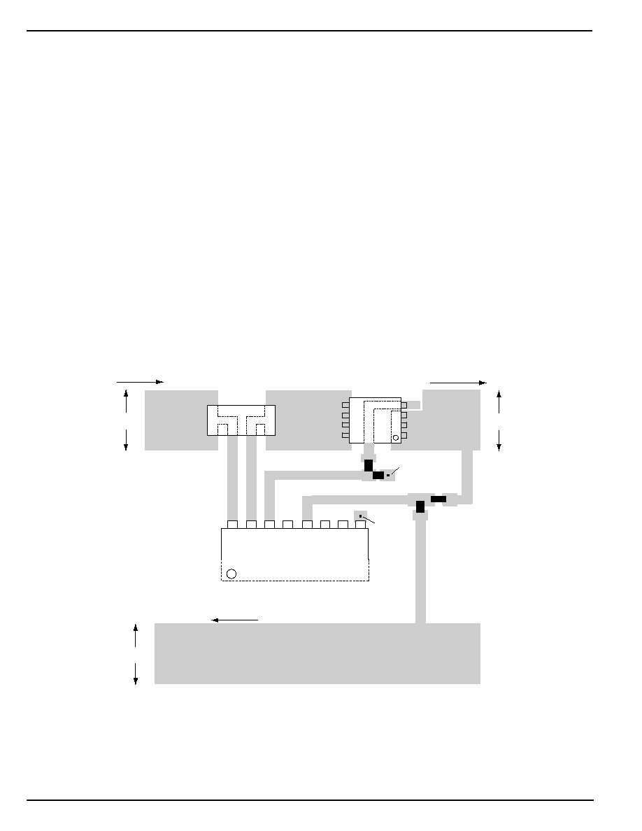
MIC2584/2585
Micrel
MIC2584/2585
26
March 2005
PCB Layout Considerations
Because of the low values of the sense resistors used with the
MIC2584/85 controllers, special attention to the layout must
be used in order for the device's circuit breaker function to
operate properly. Specifically, the use of a 4-wire Kelvin
connection to accurately measure the voltage across R
SENSE
is highly recommended. Kelvin sensing is simply a means of
making sure that any voltage drops in the power traces
connecting to the resistors does not get picked up by the
traces themselves. Additionally, these Kelvin connections
should be isolated from all other signal traces to avoid
introducing noise onto these sensitive nodes. Figure 14
illustrates a recommended, multi-layer layout for the R
SENSE
,
Power MOSFET, timer(s), and feedback network connec-
tions. The feedback network resistor values are selected for
a 12V application. Many hot swap applications will require
load currents of several amperes. Therefore, the power (V
CC
and Return) trace widths (W) need to be wide enough to allow
the current to flow while the rise in temperature for a given
copper plate (e.g., 1oz. or 2oz.) is kept to a maximum of
10
∞
C ~ 25
∞
C. Also, these traces should be as short as
possible in order to minimize the IR drops between the input
and the load. For a starting point, there are many trace width
calculation tools available on the web such as the following
link:
h t t p : / / w w w . a r a c n e t . c o m / c g i - u s r / g p a t r i c k / t r a c e . p l
Finally, the use of plated-through vias will be needed to make
circuit connections to power and ground planes when utilizing
multi-layer PC boards.
Via to
GND plane
MIC2584
VCC1
SENSE1
GA
TE1
FB1
S
S
S
G
D
D
D
D
**C
GATE
Via to
GND plane
**R
GATE
93.1k
1%
12.4k
1%
*POWER MOSFET
(SO-8)
*SENSE RESISTOR
(2512)
W
Current Flow
to the Load
Current Flow
from the Load
Current Flow
to the Load
DRAWING IS NOT TO SCALE
Similar considerations should be used for Channel 2.
*See Table 5 for part numbers and vendors.
**Optional components.
Trace width (W) guidelines given in "PCB Layout Recommendations" section of the datasheet.
OUT1
/POR
/F
A
U
L
T
GND
W
W
9
10
11
12
16
15
14
13
Figure 14. Recommended PCB Layout for Sense Resistor, Power MOSFET and Feedback Network

March 2005
27
MIC2584/2585
MIC2584/2585
Micrel
MOSFET and Sense Resistor Vendors
Device types and manufacturer contact information for power
MOSFETs and sense resistors is provided in Table 5. Some
of the recommended MOSFETs include a metal heat sink on
the bottom side of the package that is connected to the drain
leads. The recommended trace for the MOSFET gate of
Figure 14 must be redirected when using MOSFETs pack-
aged in this style. Contact the device manufacturer for
package information.
MOSFET Vendors
Key MOSFET Type(s)
*Applications
Contact Information
Vishay (Siliconix)
Si4420DY (SO-8 package)
I
OUT
10A
www.siliconix.com
Si4442DY (SO-8 package)
I
OUT
= 10A-15A, V
CC
5V
(203) 452-5664
Si3442DV (SO-8 package)
I
OUT
3A, V
CC
5V
Si7860DP (PowerPAKTM SO-8)
I
OUT
12A
Si7892DP (PowerPAKTM SO-8)
I
OUT
15A
Si7884DP (PowerPAKTM SO-8)
I
OUT
15A
SUB60N06-18 (TO-263)
I
OUT
20A, V
CC
5V
SUB70N04-10 (TO-263)
I
OUT
20A, V
CC
5V
International Rectifier
IRF7413 (SO-8 package)
I
OUT
10A
www.irf.com
IRF7457 (SO-8 package)
I
OUT
10A
(310) 322-3331
IRF7822 (SO-8 package)
I
OUT
= 10A-15A, V
CC
5V
IRLBA1304 (Super220TM)
I
OUT
20A, V
CC
5V
Fairchild Semiconductor
FDS6680A (SO-8 package)
I
OUT
10A
www.fairchildsemi.com
FDS6690A (SO-8 package)
I
OUT
10A, V
CC
5V
(207) 775-8100
Philips
PH3230 (SOT669-LFPAK)
I
OUT
20A
www.philips.com
Hitachi
HAT2099H (LFPAK)
I
OUT
20A
www.halsp.hitachi.com
(408) 433-1990
* These devices are not limited to these conditions in many cases, but these conditions are provided as a helpful reference for customer applications.
Resistor Vendors
Sense Resistors
Contact Information
Vishay (Dale)
"WSL" Series
www.vishay.com/docswsl_30100.pdf
(203) 452-5664
IRC
"OARS" Series
www.irctt.com/pdf_files/OARS.pdf
"LR" Series
www.irctt.com/pdf_files/LRC.pdf
(second source to "WSL")
(828) 264-8861
Table 5. MOSFET and Sense Resistor Vendors

MIC2584/2585
Micrel
MIC2584/2585
28
March 2005
Package Information
Rev. 01
16-Pin TSSOP (TS)
1.10 MAX (0.043)
0.15 (0.006)
0.05 (0.002)
1.00 (0.039) REF
8
∞
0
∞
6.4 BSC (0.252)
7.90 (0.311)
7.70 (0.303)
0.30 (0.012)
0.19 (0.007)
0.20 (0.008)
0.09 (0.003)
0.70 (0.028)
0.50 (0.020)
DIMENSIONS:
MM (INCH)
4.50 (0.177)
4.30 (0.169)
0.65 BSC
(0.026)
24-Pin TSSOP (TS)
MICREL, INC.
2180 FORTUNE DRIVE
SAN JOSE, CA 95131
USA
TEL
+ 1 (408) 944-0800
FAX
+ 1 (408) 474-1000
WEB
http://www.micrel.com
The information furnished by Micrel in this datasheet is believed to be accurate and reliable. However, no responsibility is assumed by Micrel for its use.
Micrel reserves the right to change circuitry and specifications at any time without notification to the customer.
Micrel Products are not designed or authorized for use as components in life support appliances, devices or systems where malfunction of a product can
reasonably be expected to result in personal injury. Life support devices or systems are devices or systems that (a) are intended for surgical implant into
the body or (b) support or sustain life, and whose failure to perform can be reasonably expected to result in a significant injury to the user. A Purchaser's
use or sale of Micrel Products for use in life support appliances, devices or systems is at Purchaser's own risk and Purchaser agrees to fully indemnify
Micrel for any damages resulting from such use or sale.
© 2005 Micrel, Incorporated.