MIC2586/MIC2586R
Single-Channel, Positive High-Voltage
Hot Swap Controller/Sequencer
Power, Connect and Protect is a trademark of Micrel, Inc
Micrel, Inc ∑ 2180 Fortune Drive ∑ San Jose, CA 95131 ∑ USA ∑ tel +1 (408) 944-0800 ∑ fax +1 (408) 474-1000 ∑ http://www.micrel.com
October 2004
1
M9999-102204
(408) 955-1690
General Description
The MIC2586 and MIC2586R are single-channel positive
voltage hot swap controllers/sequencers designed to provide
safe insertion and removal of boards for systems that require
live (always-powered) backplanes. These devices use few
external components and act as controllers for external N-
channel power MOSFET devices to provide inrush current
control and output voltage slew rate control. Overcurrent
fault protection is provided via programmable analog
foldback current limit circuitry equipped with a programmable
overcurrent filter. These protection circuits combine to limit
the power dissipation of the external MOSFET to insure that
the MOSFET is in its SOA during fault conditions. The
MIC2586 provides a circuit breaker function that latches the
output MOSFET off if the load current exceeds the current
limit threshold for the duration of the programmable timer.
Conversely, the MIC2586R will attempt to restart power after
a load current fault with a low duty cycle to prevent the
MOSFET from overheating. Each device provides either an
active-HIGH (-1BM) or an active-LOW (-2BM) "Power-is-
Good" signal. The MIC2586 and the MIC2586R provide up
to three, time-sequenced "Power-is-Good" outputs that can
be used as a control for dc-dc converter circuits or power
modules.
Data sheets and support documentation can be found on
Micrel's web site at
www.micrel.com
.
Features
∑
Operates from +10V to +80V with 100V ABS MAX
operation
∑
Industrial temperature specifications at V
CC
= +24V and
V
CC
= +48V
∑
Programmable current limit with analog foldback
∑
Active current regulation minimizes inrush current
∑
Electronic circuit breaker for overcurrent fault protection
-
Output latch off (MIC2586) or
-
Output auto-retry (MIC2586R)
∑
Fast responding circuit breaker (< 2
µ
s) to short circuit
loads
∑
Programmable input undervoltage lockout
∑
Fault Reporting:
Three Open-drain "Power-is-Good" outputs for enabling
DC/DC converter(s)
-
Active-HIGH: MIC2586-1/MIC2586R-1
-
Active-LOW: MIC2586-2/MIC2586R-2
Applications
∑
General-purpose hot board insertion
∑
High-voltage, high-side electronic circuit breaker
∑
+12V/+24V/+48V Distributed Power Systems
∑
+24V/+48V Industrial/Alarm Systems
∑
Telecom Systems
∑
Medical systems
________________________________________________________________________________________________________________
Ordering Information
Part Number
Standard Pb-Free
PWRGD Polarity
Circuit Breaker Function
Package
MIC2586-1BM MIC2586-1YM Active-HIGH
Latched
14 pin SOIC
MIC2586-2BM
MIC2586-2YM
Active-LOW
Latched
14 pin SOIC
MIC2586R-1BM MIC2586R-1YM
Active- HIGH
Auto-retry
14 pin SOIC
MIC2586R-2BM MIC2586R-2YM
Active-LOW
Auto-retry
14 pin SOIC
________________________________________________________________________________________________________________
Micrel
MIC2586/MIC2586R
Power, Connect and Protect is a trademark of Micrel, Inc
Micrel, Inc ∑ 2180 Fortune Drive ∑ San Jose, CA 95131 ∑ USA ∑ tel +1 (408) 944-0800 ∑ fax +1 (408) 474-1000 ∑ http://www.micrel.com
October 2004
2
M9999-102204
(408) 955-1690
Typical Application
MIC2586/86R Typical Application Circuit
Pin Configuration
14-Pin SOIC (M)
MIC2586-1BM
MIC2586R-1BM
14-Pin SOIC (M)
MIC2586-1BM
MIC2586R-1BM

Micrel
MIC2586/MIC2586R
October 2004
3
M9999-102204
(408) 955-1690
Pin Description
Pin Number
Pin Name
Pin Function
1
8
12
NC
Reserved: Make no external connections to these pins.
2 ON
Enable Input: When the voltage at the ON pin is higher than the V
ONH
threshold,
a start cycle is initiated. An internal current source (I
GATEON
) is activated which
charges the GATE pin, ramping up the voltage at this pin to turn on an external
MOSFET. Whenever the voltage at the ON pin is lower than the V
ONL
threshold,
an undervoltage lockout condition is detected and the I
GATEON
current source is
disabled while the GATE pin is pulled low by another internal current source
(I
GATEOFF
). After a load current fault, toggling the ON pin LOW will reset the
circuit breaker then back HIGH (ON pin) will initiate another start cycle.
3 FB
Output Voltage Feedback Input: This pin is connected to an external resistor
divider that is used to sample the output load voltage. The voltage at this pin is
measured against an internal comparator whose output controls the PWRGD (or
/PWRGD) signal. PWRGD (or /PWRGD) asserts when the FB pin voltage
crosses the V
FBH
threshold. When the FB pin voltage is lower than its V
FBL
threshold, PWRGD (or /PWRGD) is deasserted. The FB comparator exhibits a
typical hysteresis of 80mV.
The FB pin voltage also affects the MIC2586/MIC2586R's foldback current limit
operation (see the "Functional Description" section for further information).
4 PWRGD1
(MIC2586-1)
(MIC2586R-1)
Active-HIGH
/PWRGD1
(MIC2586-2)
(MIC2586R-2)
Active-LOW
Power-is-Good (PWRGD1 or /PWRGD1), Open-drain Output: This pin remains
deasserted during start up while the FB pin voltage is below the V
FBH
threshold.
Once the voltage at the FB pin rises above the V
FBH
threshold, the Power-is-
Good output asserts with minimal delay (typically
5
µ
s).
For the (-1) options, the PWRGDx output pin will be high-impedance when the
FB pin voltage is higher than V
FBH
and will pull down to GND when the FB pin
voltage is less than V
FBL
.
For the (-2) options, the /PWRGDx output pin will be high-impedance when the
FB pin voltage is lower than V
FBL
and will pull down to GND when the FB pin
voltage is higher than V
FBH
.
Each Power-is-Good output pin is connected to an open-drain, N-channel
transistor implemented with high-voltage structures. These transistors are
capable of operating with pull-up resistors to supply voltages as high as 100V.
To use this signal as a logic control in low-voltage dc-dc conversion applications,
an external pull-up resistor between this pin and the logic supply voltage is
recommended, unless an internal pull-up impedance is provided by the dc-dc
module or other device (load).
5 PWRGD2
(MIC2586-1)
(MIC2586R-1)
Active-HIGH
/PWRGD2
(MIC2586-2)
(MIC2586R-2)
Active-LOW
Power-is-Good 2 (PWRGD2 or /PWRGD2), Open-drain Output: For the (-1)
option, this output signal is asserted when the following is true: PWRGD1 =
Asserted AND the PWRGD1-to-PWRGD2 delay (t
PG(1-2)
) has elapsed, where
t
PG(1-2)
is the time delay programmed by the capacitor (C
PG
) connected to the
PGTIMER pin. Once PWRGD1 is asserted, an internal current source (I
CPG
)
begins to charge C
PG
. When the voltage on C
PG
crosses the V
PG2
threshold
(typically, 0.625V), PWRGD2 is asserted. The same description above applies
to the (-2) option. For further information, refer to the PWRGD1 and PGTIMER
pin descriptions.
To use this signal as a logic control in low-voltage dc-dc conversion applications,
an external pull-up resistor between this pin and the logic supply voltage is
recommended, unless an internal pull-up impedance is provided by the dc-dc
module or other device (load).
6
GND
Tie this pin directly to the system's analog GND plane

Micrel
MIC2586/MIC2586R
October 2004
4
M9999-102204
(408) 955-1690
Pin Description
Pin Number
Pin Name
Pin Function
7 PGTIMER
Power-is-Good Delay Timer: A capacitor (C
PG
) connected from this pin to GND
sets a delay from PWRGD1 to PWRGD2 (t
PG(1-2)
) and from PWRGD1 to
PWRGD3 (t
PG(1-3)
). An internal current source (I
CPG
) is used to charge C
PG
only
after PWRGD1 has been asserted. The same description applies to the active-
LOW (-2) output signals.
9 PWRGD3
(MIC2586-1)
(MIC2586R-1)
Active-HIGH
/PWRGD3
(MIC2586-2)
(MIC2586R-2)
Active-LOW
Power-is-Good Output 3 (PWRGD3 or /PWRGD3), Open-drain Output: For the
(-1) option, this output signal is asserted when the following is true: PWRGD1 =
Asserted AND the PWRGD1-to-PWRGD3 delay (t
PG(1-3)
) has elapsed, where
t
PG(1-3)
is the time delay programmed by the capacitor (C
PG
) connected to the
PGTIMER pin. Once PWRGD1 is asserted, an internal current source (I
CPG
)
begins to charge C
PG
. When the voltage on C
PG
crosses the V
PG3
threshold
(typically, 1.25V), PWRGD3 is asserted. The same description above applies to
the (-2) option. For further information, refer to the PWRGD1 and PGTIMER pin
descriptions.
To use this signal as a logic control in low-voltage dc-dc conversion applications,
an external pull-up resistor between this pin and the logic supply voltage is
recommended, unless an internal pull-up impedance is provided by the dc-dc
module or other device (load).
10 TIMER
Current Limit Response Timer: A capacitor connected from this pin to GND
provides overcurrent filtering to prevent nuisance "tripping" of the circuit breaker
by setting the time (t
FLT
) for which the controller is allowed to remain in current
limit. Once the MIC2586 circuit breaker trips, the output latches off. Under
normal (steady-state) operation, the TIMER pin is held to GND by an internal
3.5
µ
A current source (I
TIMERDN
). When the voltage across the external sense
resistor exceeds the V
TRIP
threshold, an internal 65
µ
A current source (I
TIMERUP
) is
activated to charge the capacitor connected to the TIMER pin. When the TIMER
pin voltage reaches the V
TIMERH
threshold, the circuit breaker is tripped pulling
the GATE pin low, the I
TIMERUP
current source is disabled, and the TIMER pin
capacitor is discharged by the I
TIMERDN
current source. When the voltage at the
TIMER pin is less than 0.5V, the MIC2586 can be restarted by toggling the ON
pin LOW then HIGH.
For the MIC2586R, the capacitor connected to the TIMER pin sets the period of
auto-retry where the duty cycle is fixed at a nominal 5%.
11 GATE
Gate Drive Output: This pin is the output of an internal charge pump connected
to the gate of an external, N-channel power MOSFET. The charge pump has
been designed to provide a minimum gate drive (
V
GATE
= V
GATE
- V
CC
) of +7.5V
over the input supply's full operating range. When the ON pin voltage is higher
than the V
ONH
threshold, a 16
µ
A current source (I
GATEON
) charges the GATE pin.
When in current limit, the output voltage at the GATE pin is adjusted so that the
voltage across the external sense resistor is held equal to V
TRIP
while the
capacitor connected to the TIMER pin charges. If the current limit condition goes
away before the TIMER pin voltage rises above the V
TIMERH
threshold, then
steady-state operation resumes.
The GATE output pin is shut down whenever: (1) the input supply voltage is
lower than the V
UVL
threshold, (2) the ON pin voltage is lower than the V
ONL
threshold, (3) the TIMER pin voltage is higher than the V
TIMERH
threshold, or (4)
the difference between the VCC and SENSE pins is greater than V
TRIP
while the
TIMER pin is grounded. For cases (3) and (4) ≠ overcurrent fault conditions ≠
the GATE is immediately pulled to ground by I
GATEFLT
, a 30mA (minimum) pull-
down current.

Micrel
MIC2586/MIC2586R
October 2004
5
M9999-102204
(408) 955-1690
Pin Number
Pin Name
Pin Function
13 SENSE
Circuit Breaker Sense Input: This pin is the (-) Kelvin sense connection for the
output supply rail. A low-valued resistor (R
SENSE
) between this pin and the VCC
pin sets the circuit breaker's current limit trip point. When the current limit
detector circuit is enabled (as well as the current limit timer), while the FB pin
voltage remains higher than 1V, the voltage across the sense resistor (V
CC
-
V
SENSE
) will be regulated to V
TRIP
(47mV, typically) to maintain a constant current
into the load. When the FB pin voltage is less than
0.8V, the voltage across the
sense resistor decreases linearly to a minimum of 12mV (typical) when the FB
pin voltage is at 0V.
To disable the circuit breaker (and defeat all current limit protections), the
SENSE pin and the VCC pin can be tied together.
14 VCC
Positive Supply Voltage Input: This pin is the (+) Kelvin sense connection for the
output supply rail. The nominal operating voltage range for the MIC2586 and the
MIC2586R is +10V to +80V, and VCC can withstand input transients up to
+100V. An undervoltage lockout circuit holds the GATE pin low whenever the
supply voltage to the MIC2586/MIC2586R is less than the V
UVH
threshold.
Micrel
MIC2586/MIC2586R
October 2004
6
M9999-102204
(408) 955-1690
Absolute Maximum Ratings
(1)
(All voltages are referred to GND)
Supply Voltage (VCC) pin .............................. ≠0.3V to +100V
GATE pin........................................................ ≠0.3V to +100V
ON, SENSE pins ............................................ ≠0.3V to +100V
PWRGDx, /PWRGDx pins ............................. ≠0.3V to +100V
FB pin............................................................. ≠0.3V to +100V
TIMER, CPG pins............................................... ≠0.3V to +6V
ESD Rating
Human
Body
Model .................................................... 2kV
Machine
Model ......................................................... 200V
Lead Temperature (Soldering)
Standard Package (-xBM)
IR Reflow ........................................240
∞
C + 0
∞
C/-5
∞
C
Lead-Free Package (-xYM)
IR Reflow........................................260
∞
C + 0
∞
C/-5
∞
C
Operating Ratings
(2)
Supply Voltage (V
CC
)......................................... +10V to +80V
Ambient Temperature Range (T
A
) ..................-40
∞
C to +85∞C
Junction Temperature (T
J
) .......................................... +125∞C
Package Thermal Resistance (
JA
)
14-pin
SOIC .......................................................120 ∞C/W
DC Electrical Characteristics
(4)
V
CC
= +24V and +48V, T
A
= 25
∞
C, unless otherwise noted. BOLD indicates specifications apply over the full operating
temperature range of -40
∞
C to +85
∞
C.
Symbol Parameter
Condition
Min Typ Max Units
V
CC
Supply Voltage
10
80
V
I
CC
Supply Current
2
5
mA
V
UVH
V
UVL
Supply Voltage Undervoltage Lockout
V
CC
rising
V
CC
falling
7.5
7.0
8.0
7.5
8.5
8.0
V
V
V
HYSLO
VCC Undervoltage Lockout Hysteresis
500
mV
V
FBH
Feedback Pin Voltage High Threshold
FB Low-to-High transition
1.280
1.313
1.345
V
V
FBL
Feedback Pin Voltage Low Threshold
FB High-to-Low transition
1.208
1.233
1.258
V
V
HYSFB
Feedback Voltage Hysteresis
80
mV
V
FB
FB Pin Threshold Line Regulation
10V
V
CC
80V
-0.05
0.05
mV/V
I
FB
FB Pin Input Current
0V
V
FB
3V
-1
1
µ
A
V
TRIP
Circuit Breaker Trip Voltage, V
CC
-V
SENSE
V
FB
= 0V (See Fig. 1)
V
FB
= 1V (See Fig. 1)
5
39
12
47
17
55
mV
mV
V
GATE
MOSFET Gate Drive, V
GATE
-V
CC
+10V
Vcc
+80V
7.5
18
V
I
GATEON
GATE Pin Pull-up Current
Start cycle, V
GATE
= 7V
-10
-16
-22
µ
A
I
GATEFLT
GATE Pin rapid pull-down current (in
fault condition, until VGATE =
VGATE[TH])
(V
CC
- V
SENSE
) = (V
TRIP
+ 10mV)
V
GATE
= 5V
30
80
200
mA
I
GATEOFF
GATE Pin Turn-off Current
Normal turn-off, or from V
GATE[TH]
(MOSFET) to 0V after a fault condition
1.8 mA
I
TIMERUP
TIMER Pin Charging Current
(V
CC
≠ V
SENSE
) > V
TRIP
V
TIMER
= 0V
-24
-65
-120
µ
A
I
TIMERDN
TIMER Pin Pull-down current
(V
CC
≠ V
SENSE
) < V
TRIP
V
TIMER
= 0.6V
1.5
3.5
5
µ
A
V
TIMERH
TIMER Pin High Threshold Voltage
1.280
1.313
1.345
V

Micrel
MIC2586/MIC2586R
October 2004
7
M9999-102204
(408) 955-1690
Symbol Parameter
Condition
Min Typ Max Units
V
TIMERL
TIMER Pin Low Threshold Voltage
0.4
0.49
0.6
V
V
ONH
ON Pin High Threshold Voltage
ON Low-to-High transition
1.280
1.313
1.355
V
V
ONL
ON Pin Low Threshold Voltage
ON High-to-Low transition
1.208
1.233
1.258
V
V
HYSON
ON Pin Hysteresis
80
mV
I
ON
ON Pin Input Current
0V
V
ON
80V
2
µ
A
V
OL
Power-Good Output Voltage
PWRGDx or /PWRGDx = LOW
I
OL
= 1.6 mA
I
OL
= 4 mA
0.4
0.8
V
V
I
OFF
Power-Good Leakage Current
PWRGDx or /PWRGDx = Open-Drain
V
PGx
= V
CC
, V
ON
= 1.5V
10
µ
A
I
CPG
Power-Good Delay Capacitor Charging
Current
V
PGTIMER
= 0.6V
V
CC
=10V, 24V, 48V, 80V
4
7
10
µ
A
V
PG2
PGTIMER Threshold Voltage to Assert
PWRGD2 (MIC2586/86R-1) or
/PWRGD2 (MIC2586/86R-2)
0.5
0.625
0.7
V
V
PG3
PGTIMER Threshold Voltage to Assert
PWRGD3 (MIC2586/86R-1) or
/PWRGD2 (MIC2586/86R-2)
1.04
1.25
1.46
V
AC Electrical Characteristics
(4)
V
CC
= +24V and +48V, T
A
= 25
∞
C, unless otherwise noted. BOLD indicates specifications apply over the full operating temperature range of -
40
∞
C to +85
∞
C.
Symbol Parameter
Condition
Min Typ Max Units
t
PONLH
ON High to GATE High
IRF530, C
GATE
= 10nF
3
ms
t
PONHL
ON Low to GATE Low
V
IN
= 48V, IRF530, C
GATE
= 10nF
1
ms
t
PFBLH
FB Valid to PWRGDx High
(MIC2586/86R-1)
R
PG
= 50k
pull-up to 48V, C
L
=100pF
2
µ
s
t
PFBHL
FB Invalid to PWRGDx Low
(MIC2586/86R-1)
R
PG
= 50k
pull-up to 48V, C
L
=100pF
4
µ
s
t
PFBHL
FB Valid to /PWRGDx Low
(MIC2586/86R-2)
R
PG
= 50k
pull-up to 48V, C
L
=100pF
4
µ
s
t
PFBLH
FB Invalid to /PWRGDx High
(MIC2586/86R-2)
R
PG
= 50k
pull-up to 48V, C
L
=100pF
2
µ
s
t
PG(1-2)
Delay from PWRGD1 to PWRGD2 or
Delay from /PWRGD1 to /PWRGD2
C
PG
= 0.1
µ
F
21 ms
t
PG(1-3)
Delay from PWRGD1 to PWRGD3 or
Delay from /PWRGD1 to /PWRGD3
C
PG
= 0.1
µ
F
42 ms
t
OCSENSE
Overcurrent Sense to GATE Low
Trip Time
(V
CC
- V
SENSE
) = (V
TRIP
+ 10mV)
Figure 7
1 2
µ
s
Notes:
1.
Exceeding the absolute maximum rating may damage the device.
2.
The device is not guaranteed to function outside its operating rating.
3.
Devices are ESD sensitive. Handling precautions recommended. Human body model, 1.5k in series with 100pF.
4.
Specification for packaged product only.
Micrel
MIC2586/MIC2586R
Power, Connect and Protect is a trademark of Micrel, Inc
Micrel, Inc ∑ 2180 Fortune Drive ∑ San Jose, CA 95131 ∑ USA ∑ tel +1 (408) 944-0800 ∑ fax +1 (408) 474-1000 ∑ http://www.micrel.com
October 2004
8
M9999-102204
(408) 955-1690
Timing Diagrams
Figure 1. Foldback Current Limit Transfer Characteristic
Figure 2. ON to GATE Timing
Figure 3. MIC2586/86R-1 FB to PWRGD1 Timing
Figure 4. MIC2586/86R-2 FB to /PWRGD1 Timing
Figure 5. MIC2586/86R-1 Multiple PWRGDx Timing
Figure 6. MIC2586/86R-2 Multiple /PWRGDx Timing
Figure 7. Overcurrent Sense to GATE Timing
Micrel
MIC2586/MIC2586R
October 2004
9
M9999-102204
(408) 955-1690
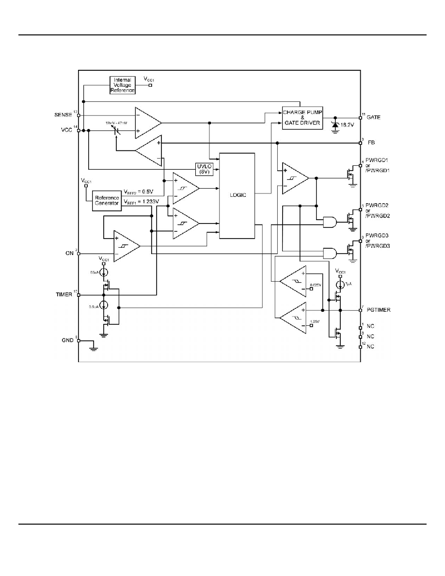
Functional Characteristics
MIC2586/MIC2586R Block Diagram

Micrel
MIC2586/MIC2586R
October 2004
10
M9999-102204
(408) 955-1690
Functional Description
Hot Swap Insertion
When circuit boards are inserted into systems carrying live
supply voltages ("hot swapped"), high inrush currents often
result due to the charging of bulk capacitance that resides
across the circuit board's supply pins. These current spikes
can cause the system's supply voltages to temporarily go out
of regulation causing data loss or system lock-up. In more
extreme cases, the transients occurring during a hot swap
event may cause permanent damage to connectors or on-
board components.
The MIC2586/MIC2586R is designed to address these
issues by limiting the maximum current that is allowed to flow
during hot swap events. This is achieved by implementing a
constant-current control loop at turn-on. In addition to inrush
current control, the MIC2586 and MIC2586R incorporate
input voltage supervisory functions and user-programmable
overcurrent protection, thereby providing robust protection for
both the system and the circuit board.
Input Supply Transient Suppression and Filtering
The MIC2586/MIC2586R is guaranteed to withstand
transient voltage spikes up to 100V. However, voltage
spikes in excess of 100V may cause damage to the
controller. In order to suppress transients caused by
parasitic inductances, wide (and short) power traces should
be utilized. Alternatively, a heavier trace plating will help
minimize inductive spikes that may arise during events (e.g.,
short circuit loads) that can cause a large di/dt to occur.
External surge protection, such as a clamping diode, is also
recommended as an added safeguard for device (and
system) protection. Lastly, a 0.1
µ
F filter capacitor is
recommended to help reject additional noise.
Start-Up Cycle
When the power supply voltage to the MIC2586/MIC2586R is
higher than the V
UVH
and the V
ONH
threshold voltages, a start
cycle is initiated. When the controller is enabled, an internal
16
µ
A current source (I
GATEON
) is enabled and the GATE pin
voltage rises from 0V with respect to ground at a rate equal
to:
dV
GATE
dt
=
I
GATEON
C
GATE
(1)
The internal charge pump has sufficient output drive to fully
enhance commonly available power MOSFETs for the lowest
possible DC losses. The gate drive is guaranteed to be
between 7.5V and 18V over the entire supply voltage
operating range (10V to 80V), so 60V BV
DSS
and 30V BV
DSS
N-channel power MOSFETs can be used for +48V and +24V
applications, respectively. However, an external Zener diode
(18-V) connected from the source to the gate as shown in the
"Typical Applications" circuit is highly recommended. A good
choice for an 18-V Zener diode in this application is the
MMSZ5248B, available in a small SOD123 package.
C
GATE
is used to adjust the GATE voltage slew rate while R3
minimizes the potential for high-frequency parasitic
oscillations from occurring in M1. However, note that
resistance in this part of the circuit has a slight destabilizing
effect upon the MIC2586/MIC2586R's current regulation
loop. Compensation resistor R4 is necessary for stabilization
of the current regulation loop. The current through the power
transistor during initial inrush is given by:
I
INRUSH
=
C
LOAD
◊
I
GATEON
C
GATE
(2)
The drain current of the MOSFET is monitored via an
external current sense resistor to ensure that it never
exceeds the programmed threshold, as described in the
"Circuit Breaker Operation" section.
A capacitor connected to the controller's TIMER pin sets the
value of overcurrent detector delay, t
FLT
, which is the time for
which an overcurrent event must last to signal a fault
condition and to cause an output latch-off. These devices will
be driving a capacitive load in most applications, so a
properly chosen value of C
TIMER
prevents false-, or nuisance-,
tripping at turn-on as well as providing immunity to noise
spikes after the start-up cycle is complete. The procedure for
selecting a value for C
TIMER
is given in the "Circuit Breaker
Operation" section.
Overcurrent Protection
The MIC2586 and the MIC2586R use an external, low-value
resistor in series with the drain of the external MOSFET to
measure the current flowing into the load. The VCC
connection (Pin 14) and the SENSE connection (Pin 13) are
the (+) and (-) inputs, respectively, of the device's internal
current sensing circuits. Kelvin sense connections are
strongly recommended for sensing the voltage across these
pins. See the "Applications Information" for further details.
The nominal current limit is determined by the following
equation.
SENSE
TRIP(TYP)
LIMIT
R
V
I
=
(3)
where V
TRIP(TYP)
is the typical current limit threshold specified
in the datasheet and R
SENSE
is the value of the selected
sense resistor. As the MIC2586 and the MIC2586R employ
a constant-current regulation scheme in current limit, the
charge pump's output voltage at the GATE pin is adjusted so
that the voltage across the external sense resistor is held
equal to V
TRIP
while the capacitor connected to the TIMER
pin is being charged. If the current-limit condition goes away
before the TIMER pin voltage rises above the V
TIMERH
threshold, then steady-state operation resumes. To prevent
excessive power dissipation in the external MOSFET under
load current fault conditions, the FB pin voltage is used as

Micrel
MIC2586/MIC2586R
October 2004
11
M9999-102204
(408) 955-1690
the control element in a circuit that lowers the current limit as
a function of the output voltage. When the load current
increases to the point where the output voltage at the load
approaches 0V (likewise, the MIC2586/MIC2586R's FB pin
voltage also approaches 0V), the result is a proportionate
decrease in the maximum current allowed into the load. This
foldback current limit subcircuit's transfer characteristic is
shown in Figure 1. Under excessive load conditions (output
and FB voltage equals 0V), the foldback current limiting
circuit controls the MIC2586/MIC2586R's GATE drive to
force a constant 12mV (typical) voltage drop across the
external sense resistor.
Circuit Breaker Operation
The MIC2586/MIC2586R employ an electronic circuit breaker
that protects the external N-channel power MOSFET and
other system components against large-scale output current
faults, both during initial card insertion or during steady-state
operation. The current-limit threshold is set via an external
resistor, R
SENSE
, connected between the circuit's V
CC
pin and
SENSE pin. For the MIC2586/MIC2586R, a fault current
timing circuit is set via an external capacitor (C
TIMER
) that
determines the length of the time delay (t
FLT
) for which the
controller remains in current limit before the circuit breaker is
tripped. Programming the response time of the overcurrent
detector helps to prevent nuisance tripping of the circuit
breaker because of high inrush currents charging bulk and
distributed capacitive loads. The nominal ovecurrent
response time is calculated using the following equation:
TIMERUP
TIMERH
FILTER
FLT
I
V
C
(ms)
t
◊
=
)
F
(
C
20
(ms)
t
FILTER
FLT
µ
◊
=
(4)
Whenever the voltage across R
SENSE
exceeds the
MIC2586/MIC2586R's nominal circuit breaker threshold
voltage of 47mV during steady-state operation, two things
occur:
1. A constant-current regulation loop will engage within
1µs after an overcurrent condition is detected by
R
SENSE
, and the control loop is designed to hold the
voltage across R
SENSE
equal to 47mV. This feature
protects both the load and the MIC2586/MIC2586R
circuits from excessively high currents.
2. Capacitor C
TIMER
is then charged up to the V
TIMERH
threshold (1.313V) by an internal 65µA current
source (I
TIMERUP
). If the excessive current persists
such that the voltage across C
TIMER
crosses the
V
TIMERH
threshold, the circuit breaker trips and the
GATE pin is immediately pulled low by a 30mA
(minimum) internal current sink. This operation turns
off the MOSFET quickly and disconnects the input
from the load. The value of C
TIMER
should be selected
to allow the circuit's minimum regulated output
current (I
OUT
) to equal I
LIMIT
for somewhat longer than
the time it takes to charge the total load capacitance.
An initial value for C
TIMER
is found by calculating the time it
will take for the MIC2586/MIC2586R to completely charge up
the output capacitive load. Assuming the load is enabled by
the PWRGDx (or /PWRGDx) signal(s) of the controller, the
turn-on delay time is derived from the following expression, I
= C
◊
(dV/dt):
t
TURN-ON
=
C
LOAD
◊
V
CC(MAX)
I
LIMIT
(5)
Using parametric values for the MIC2586/MIC2586R, an
expression relating a worse-case design value for C
TIMER
,
using the MIC2586/MIC2586R specification limits, to the
circuit's turn-on delay time is:
)
TIMERH(MIN
X)
TIMERUP(MA
ON
-
TURN
TIMER(MAX)
V
I
t
C
◊
=
◊
=
1.280V
A
120
t
C
ON
-
TURN
TIMER(MAX)
µ
◊
◊
=
sec
F
10
94
t
C
6
-
ON
-
TURN
(MAX)
TIMER
µ
(6)
For example, in a system with a C
LOAD
= 1000µF, a maximum
V
CC
= +72V, and a maximum load current on a nominal +48V
buss of 1.65A, the nominal circuit design equations steps
are:
1. Choose
I
LIMIT
= I
HOT_SWAP(nom)
= 2A (1.65A + 20%);
2. Select an R
SENSE
(Closest 1% standard value is
19.6m
);
3. Using
I
CHARGE
= I
LIMIT
= 2A, the application circuit turn-
on time is calculated using Equation 5:
t
TURN-ON
=
1000
µ
F
◊
72V
(
)
2A
=
36ms
Allowing for capacitor tolerances and a nominal 36ms turn-on
time, an initial worse-case value for C
TIMER
is:
F
3.38
sec
F
10
94
0.036s
C
6
-
TIMER(MAX)
µ
µ
=
◊
◊
=
The closest standard ±5% tolerance capacitor value is 3.3µF
and would be a good initial starting value for prototyping.
Whenever the MIC2586 is not in current limit, C
TIMER
is
discharged to GND by an internal 3.5µA current sink
(I
TIMERDN
).
For the MIC2586R, the circuit breaker automatically resets
after (20) t
FLT_AUTO
time constants. If the fault condition still
exists, capacitor C
TIMER
will begin to charge up to the V
TIMERH
threshold, and if exceeded, trip the circuit breaker. Capacitor
C
TIMER
will then be discharged by I
TIMERDN
until the voltage
across C
TIMER
drops below the V
TIMERL
threshold, at which
time another start cycle is initiated. This will continue until
either of the following occurs: a) the fault condition is
removed, b) the input supply voltage power is

Micrel
MIC2586/MIC2586R
October 2004
12
M9999-102204
(408) 955-1690
)
removed/cycled, or c) the ON pin is toggled LOW then HIGH.
The duty cycle of the auto-restart function is therefore fixed
at 5% and the period of the auto-restart cycle is given by:
FLT_AUTO
RT
AUTO_RESTA
t
20
t
◊
=
(
) (
TIMERUP
TIMERL
TIMERH
TIMER
RESTART
-
AUTO
I
V
V
C
20
t
-
◊
◊
=
◊
=
F
ms
250
C
t
TIMER
RESTART
-
AUTO
µ
(7)
The auto-restart period for the example above where the
worse-case C
TIMER
was calculated to be 3.3µF is:
t
AUTO-RESTART
= 825ms
Input Undervoltage Lockout
The MIC2586/MIC2586R have an internal undervoltage
lockout circuit that inhibits operation of the controller's
internal circuitry unless the power supply voltage is stable
and within an acceptable tolerance. If the supply voltage to
the controller with respect to ground is greater than the V
UVH
threshold voltage (8V typical), the controller's internal circuits
are enabled and the controller is then ready for normal
operation pending the state of the ON pin voltage. Once in
steady-state operation, the controller's internal circuits
remain active so long as the supply voltage with respect to
ground is higher than the controller's internal V
UVL
threshold
voltage (7.5V typical).
Power-is-Good Output Signals
For the MIC2586-1/MIC2586R-1, power-good output signal
PWRGD1 will be high impedance when the FB pin voltage is
higher than the V
FBH
threshold and will pull down to GND
when the FB pin voltage is lower than the V
FBL
threshold. For
the MIC2586-2/MIC2586R-2, power-good output signal
/PWRGD1 will pull down to GND when the FB pin voltage is
higher than the V
FBH
threshold and will be high impedance
when the FB pin voltage is lower than the V
FBL
threshold.
Hence, the (-1) parts have an active-HIGH PWRGDx signal
and the (-2) parts have an active-LOW /PWRGDx output.
PWRGDx (or /PWRGDx) may be used as an enable signal
for one or more DC/DC converter modules or for other
system functions. When used as an enable signal, the time
necessary for the PWRGDx (or /PWRGDx) signal to pull-up
(when in high impedance state) will depend upon the (RC)
load at the respective Power-is-Good pin.
Power-is-Good output signals PWRGD2 (/PWRGD2) and
PWRGD3 (/PWRGD3) are asserted after the assertion of
PWRGD1 (/PWRGD1) by a user-programmable time delay
set by an external capacitor (C
PG
) from the controller's
PGTIMER pin (Pin 7) to GND. An expression for the time
delay to assert PWRGD2 (or /PWRGD2) after PWRGD1 (or
/PWRGD1) asserts is given by:
PG2
CPG
PG
2)
PG(1
V
I
C
t
◊
=
-
where V
PG2
(0.625V, typically) is the PWRGD2 (or
/PWRGD2) threshold voltage for PGTIMER and I
CPG
(7
µ
A,
typically) is the internal PGTIMER pin charging current.
Similarly, an expression for the time delay to assert
PWRGD3 (or /PWRGD3) after PWRGD1 (or /PWRGD1)
asserts is given by:
PG3
CPG
PG
3)
PG(1
V
I
C
t
◊
=
-
where V
PG3
(1.25V, typically) is the PWRGD3 (or /PWRGD3)
threshold voltage for PGTIMER. Therefore, PWRGD2 (or
/PWRGD2) will be delayed after the assertion of PWRGD1
(or /PWRGD1) by:
F)
(
C
90
(ms)
t
PG
2)
PG(1
µ
◊
-
(8)
PWRGD3 (/PWRGD3) follows the assertion of PWRGD1
(/PWRGD1) by a delay:
F)
(
C
180
(ms)
t
PG
3)
PG(1
µ
◊
-
(9)
For example, for a C
PG
of 0.1
µ
F, PWRGD2 (or /PWRGD2)
will be asserted 9ms after PWRGD1 (or /PWRGD1).
PWRGD3 (or /PWRGD3) will then be asserted 9ms after
PWRGD2 (or /PWRGD2) and 18ms after the assertion of
PWRGD1 (or /PWRGD1). The relationships between V
OUT
,
V
FBH
, PWRGD1, PWRGD2, and PWRGD3 are shown in
Figures 5 and 6.
Each Power-is-Good output pin is connected to an open-
drain, N-channel transistor implemented with high-voltage
structures. These transistors are capable of operating with
pull-up resistors to supply voltages as high as 100V.

Micrel
MIC2586/MIC2586R
October 2004
13
M9999-102204
(408) 955-1690
Applications Information
External ON/OFF Control
The MIC2586/MIC2586R have an ON pin input that is used
to enable the controller to commence a start-up sequence
upon card insertion or to disable controller operation upon
card removal. In addition, the ON pin can be used to reset
the MIC2586/MIC2586R's internal electronic circuit breaker
in the event of a load current fault. To reset the electronic
circuit breaker, the ON pin is toggled LOW then HIGH. The
ON pin is internally connected to an analog comparator with
80mV of hysteresis. When the ON pin voltage falls below its
internal V
ONL
threshold, the GATE pin is immediately pulled
low. The GATE pin will be held low until the ON pin voltage is
above its internal V
ONH
threshold. The external circuit's ON
threshold voltage level is programmed using a resistor divider
(R1 & R2) as shown in the "Typical Application" circuit. The
equations to set the trip points are shown below. For the
following example, the external circuit's ON threshold is set
to V
ONH(EX)
= +37V, a value commonly used in +48V Central
Office power distribution applications.
V
ONH(EX)
=
V
ONH
◊
R1
+
R2
R2
(10)
Given V
ONH
and R2, a value for R1 can be determined. A
suggested value for R2 is that which will provide
approximately 100
µ
A of current through the voltage divider
chain at V
CC
= V
ONH
. This yields the following as a starting
point:
R2
=
V
ONH(TYP)
100
µ
A
=
1.313V
100
µ
A
=
13.13k
The closest standard 1% value for R2 is 13k
. Now, solving
for R1 yields:
R1
=
R2
◊
V
ONH(EX)
V
ONH(TYP)
-
1
=
13k
◊
37V
1.313V
-
1
=
353.3k
The closest standard 1% value for R1 is 357k
.
Using standard 1% resistor values, the external circuit's
nominal ON and OFF thresholds are:
V
ON(EX)
= +36V
V
OFF(EX)
= +34V
In solving for V
OFF(EX)
, replace V
ONH
with V
ONL
in Equation 10.
Output Voltage Power-is-Good Detection
The MIC2586/86R includes an analog comparator used to
monitor the output voltage of the controller through an
external resistor divider as shown in the "Typical Application"
circuit. The FB input pin is connected to the non-inverting
input and is compared against an internal reference voltage.
The analog comparator exhibits a hysteresis of 80mV.
Setting the "Power-is-Good" threshold for the circuit follows a
similar approach as setting the circuit's ON/OFF input
voltage. The equations to set the trip points are shown
below. For the following +48V telecom application, power-is-
good output signal PWRGD1 (or /PWRGD1) is to be de-
asserted when the output supply voltage is lower than +48V-
10% (+43.2V).
V
OUT(NOT GOOD)
= V
FBL
◊
R5 + R6
R6
(11)
Given V
FBL
and R6, a value for R5 can be determined. A
suggested value for R6 is that which will provide
approximately 100
µ
A of current through the voltage divider
chain at V
OUT(NOT GOOD)
= V
FBL
. This yields the following
equation as a starting point:
R6
=
V
FBL(TYP)
100
µ
A
=
1.233V
100
µ
A
=
12.33k
The closest standard 1% value for R6 is 12.4k
. Now,
solving for R5 yields:
R5
=
R6
◊
V
OUT(NOT GOOD)
V
FBL(TYP)
-
1
=
12.4k
◊
43.2V
1.233V
-
1
=
422k
The closest standard 1% value for R5 is 422k
.
Using standard 1% resistor values, the external circuit's
nominal "power-is-good" and "power-is-not-good" output
voltages are:
V
OUT(GOOD)
= +46V
V
OUT(NOT GOOD)
= +43.2V
In solving for V
OUT(GOOD)
, substitute V
FBH
for V
FBL
in Equation
11.
Sense Resistor Selection
The sense resistor is nominally valued at:
OM)
HOT_SWAP(N
TRIP(TYP)
SENSE
I
V
R
=
(12)
where V
TRIP(TYP)
is the nominal circuit breaker threshold
voltage (47mV) and I
HOT_SWAP(NOM)
is the nominal inrush load
current level to trip the internal circuit breaker.
To accommodate worse-case tolerances in the sense
resistor (for a ±1% initial tolerance, allow ±3% tolerance for
variations over time and temperature) and circuit breaker
threshold voltages, a slightly more detailed calculation must
be used to determine the minimum and maximum hot swap
load currents.
The MIC2586/MIC2586R has a minimum current limit
threshold voltage of 39mV, thus the minimum hot swap load
current is determined where the sense resistor is 3% high:
I
HOT_SWAP(MIN)
=
39mV
1.03
◊
R
SENSE(NOM)
(
)
=
37.9mV
R
SENSE(NOM)
Micrel
MIC2586/MIC2586R
October 2004
14
M9999-102204
(408) 955-1690
Keep in mind that the minimum hot swap load current should
be greater than the application circuit's upper steady-state
load current boundary. Once the lower value of R
SENSE
has
been calculated, it is good practice to check the maximum
hot swap load current (I
HOT_SWAP(MAX)
), which the circuit may
let pass in the case of tolerance build-up in the opposite
direction. Here, the worse-case maximum is found using a
V
TRIP(MAX)
threshold of 55mV and a sense resistor 3% low in
value:
I
HOT_SWAP(MAX)
=
55mV
0.97
◊
R
SENSE(NOM)
(
)
=
56.7mV
R
SENSE(NOM)
In this case, the application circuit must be sturdy enough to
operate over a ~1.5-to-1 range in hot swap load currents.
For example, if an MIC2586 circuit must pass a minimum hot
swap load current of 4A without nuisance trips, R
SENSE
should
be set to:
=
=
9.75m
4A
39mV
R
SENSE(NOM)
where the nearest 1% standard value is 9.76m
. At the
other tolerance extremes, I
HOT_SWAP(MAX)
for the circuit in
question is then simply:
5.8A
9.76m
56.7mV
I
ax)
HOT_SWAP(m
=
=
With a knowledge of the application circuit's maximum hot
swap load current, the power dissipation rating of the sense
resistor can be determined using P = I
2
R. Here, The current
is I
HOT_SWAP(MAX)
= 5.8A and the resistance R
SENSE(MIN)
=
(0.97)(R
SENSE(NOM)
) = 9.47m
. Thus, the sense resistor's
maximum power dissipation is:
P
MAX
=
5.8A
(
)
2
◊
9.47m
(
)
=
0.319W
A 0.5W sense resistor is a good choice in this application.
When the MIC2586/MIC2586R's foldback current limiting
circuit is engaged in the above example, the current limit
would nominally fold back to 1.23A when the output is
shorted to ground.
PCB Layout Considerations
4-Wire Kelvin Sensing
Because of the low value typically required for the sense
resistor, special care must be used to accurately measure
the voltage drop across it. Specifically, the measurement
technique across R
SENSE
must employ 4-wire Kelvin sensing.
This is simply a means of ensuring that any voltage drops in
the power traces connected to the resistors are not picked up
by the signal conductors measuring the voltages across the
sense resistors.
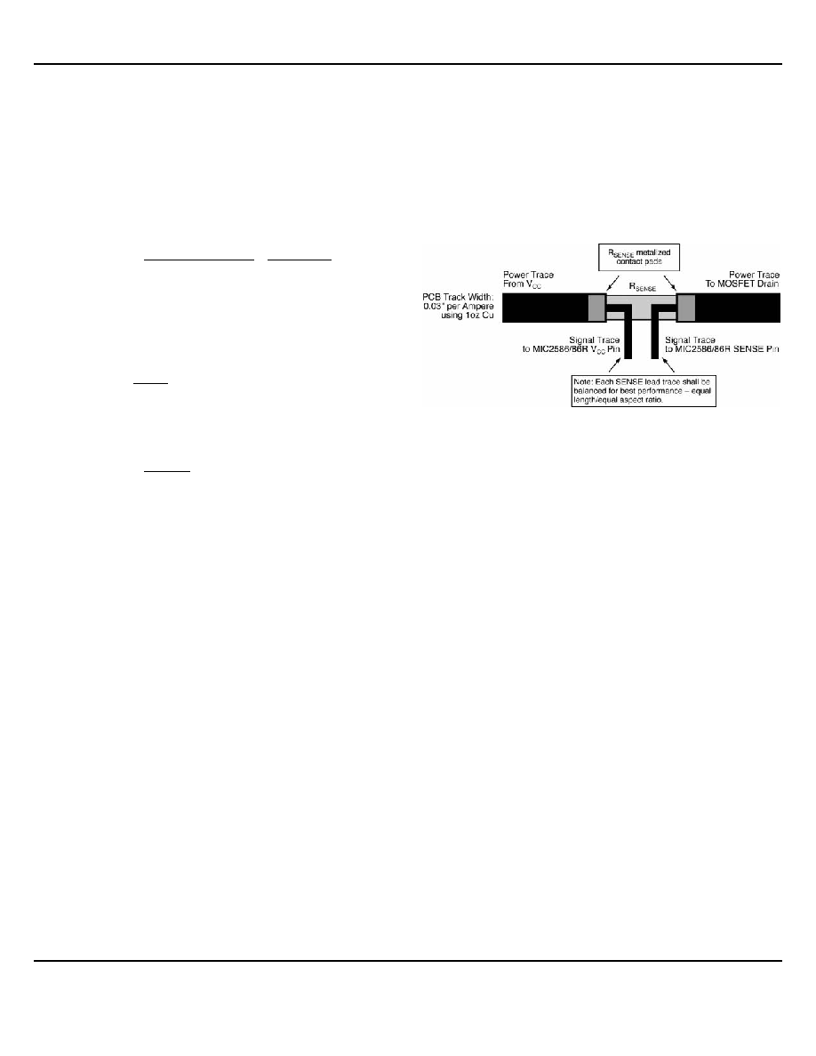
Figure 8 illustrates how to implement 4-wire Kelvin sensing.
As the figure shows, all the high current in the circuit (from
V
CC
through R
SENSE
and then to the drain of the N-channel
power MOSFET) flows directly through the power PCB traces
and through R
SENSE
. The voltage drop across R
SENSE
is
sampled in such a way that the high currents through the
power traces will not introduce significant parasitic voltage
drops in the sense leads. It is recommended to connect the
hot swap controller's sense leads directly to the sense
resistor's metalized contact pads. The Kelvin sense signal
traces should be symmetrical with equal length and width,
kept as short as possible and isolated from any noisy signals
and planes.
Figure 8. 4-Wire Kelvin Sense Connections for R
SENSE
Additionally, for designs that implement Kelvin sense
connections that exceed 1" in length and/or if the Kelvin
(signal) traces are vulnerable to noise possibly being injected
onto these signals, the example circuit shown in Figure 9 can
be implemented to combat noisy environments. This circuit
implements a 1.6 MHz low-pass filter to attenuate higher
frequency disturbances on the current sensing circuitry.
However, individual system analysis should be used to
determine if filtering is necessary and to select the
appropriate cutoff frequency for each specific application.
Other Layout Considerations
Figure 10 is a recommended PCB layout diagram for the
MIC2586-2BM. Many hot swap applications will require load
currents of several amperes. Therefore, the power (V
CC
and
Return) trace widths (W) need to be wide enough to allow the
current to flow while the rise in temperature for a given
copper plate (e.g., 1oz. or 2oz.) is kept to a maximum of
10∞C to 25∞C. Also, these traces should be as short as
possible in order to minimize the IR drops between the input
and the load. The feedback network resistor values in Figure
10 are selected for a +24V application. The resistors for the
feedback (FB) and ON pin networks should be placed close
to the controller and the associated traces should be as short
as possible to improve the circuit's noise immunity. The input
"clamping diode" (D1) is referenced in the "Typical
Application Circuit" on Page 1. If possible, use high-
frequency PCB layout techniques around the GATE circuitry
(shown in the "Typical Application Circuit") and use a dummy
resistor (e.g., R3 = 0
)
during the prototype phase. If R3 is
needed to eliminate high-frequency oscillations, common
values for R3 range between 4.7
to 20
for various power
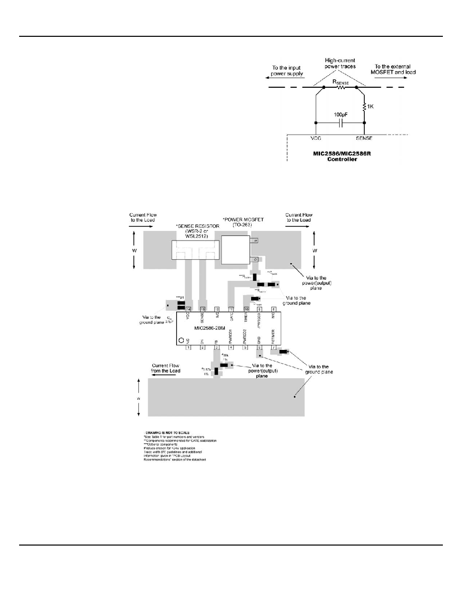
Micrel
MIC2586/MIC2586R
October 2004
15
M9999-102204
(408) 955-1690
MOSFETs. Finally, the use of plated-through vias will be
needed to make circuit connection to the power and ground
planes when utilizing multi-layer PCBs.
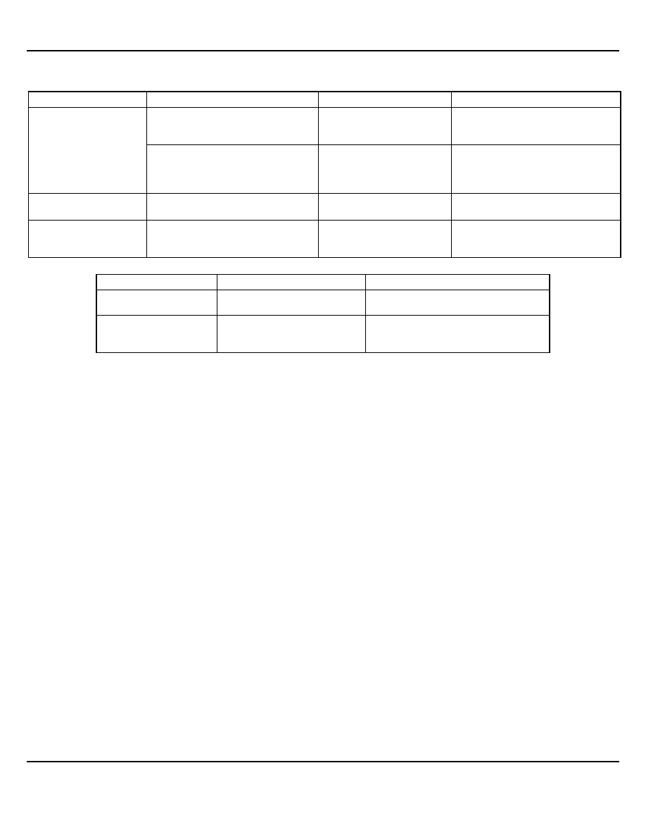
MOSFET and Sense Resistor Vendors
Device types, part numbers, and manufacturer contacts
for power MOSFETs and sense resistors are provided in
Table 1.
Figure 9. Current Limit Sense Filter for Noisy Systems
Figure 10. Recommended PCB Layout for Sense Resistor, Power MOSFET, Timer and Feedback Network.
Micrel
MIC2586/MIC2586R
October 2004
16
M9999-102204
(408) 955-1690
MOSFET Vendors
Key MOSFET Type(s)
Breakdown Voltage (V
DSS
) Contact
Information
SUM75N06-09L (TO-263)
SUM70N06-11 (TO-263)
SUM50N06-16L (TO-263)
60V
60V
60V
www.siliconix.com
(203) 452-5664
Vishay - Siliconix
SUP85N10-10 (TO-220AB)
SUB85N10-10 (TO-263)
SUM110N10-09 (TO-263)
SUM60N10-17 (TO-263)
100V
100V
100V
100V
www.siliconix.com
(203) 452-5664
International Rectifier
IRF530 (TO-220AB)
IRF540N (TO-220AB)
100V
100V
www.irf.com
(310) 322-3331
Renesas
2SK1298 (TO-3PFM)
2SK1302 (TO-220AB)
2SK1304 (TO-3P)
60V
100V
100V
www.renesas.com
(408) 433-1990
Resistor Vendors
Sense Resistors
Contact Information
Vishay - Dale
"WSL" and "WSR" Series
www.vishay.com/docswsl_30100.pdf
(203) 452-5664
IRC
"OARS" Series
"LR" Series
second source to "WSL"
www.irctt.com/pdf_files/OARS.pdf
www.irctt.com/pdf_files/LRC.pdf
(828) 264-8861
Table 1. MOSFET and Sense Resistor Vendors
Micrel
MIC2586/MIC2586R
October 2004
17
M9999-102204
(408) 955-1690
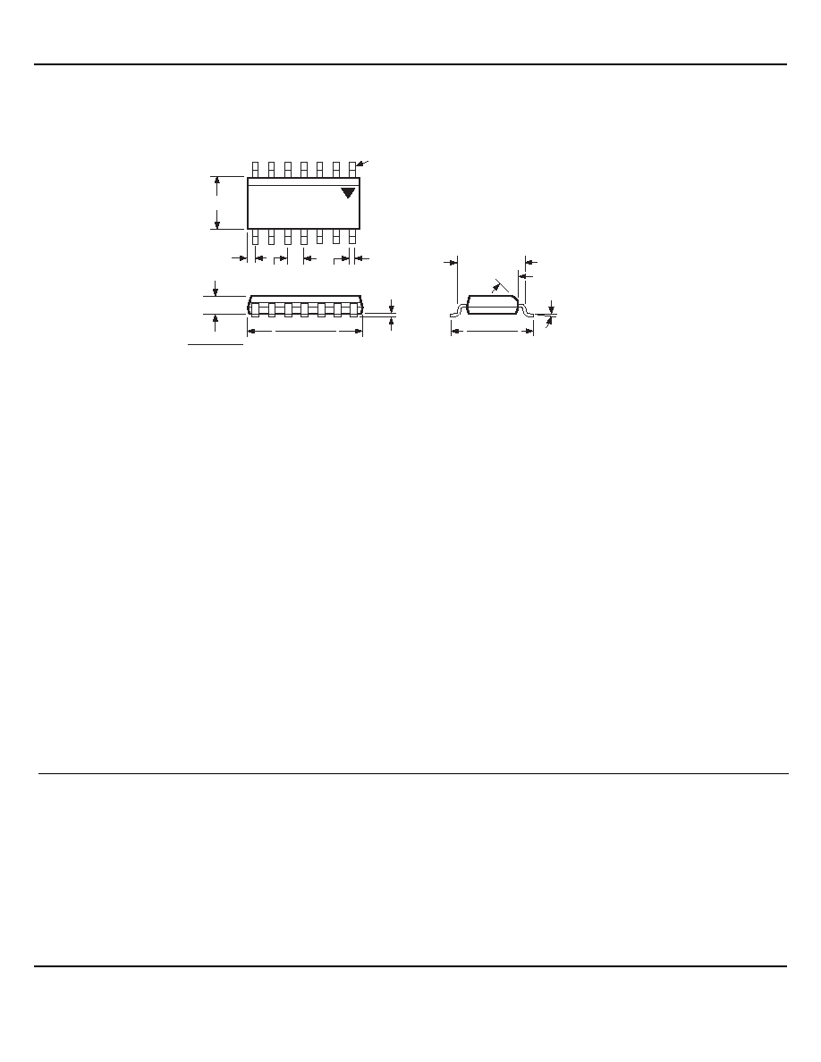
Package Information
45
∞
3
∞
≠6
∞
0.244 (6.20)
0.228 (5.80)
0.344 (8.75)
0.337 (8.55)
0.006 (0.15)
SEATING
PLANE
0.026 (0.65)
MAX
)
0.016 (0.40)
TYP
0.154 (3.90)
0.057 (1.45)
0.049 (1.25)
0.193 (4.90)
0.050 (1.27)
TYP
PIN 1
DIMENSIONS:
INCHES (MM)
14-Pin SOIC (M)
MICREL, INC. 1849 FORTUNE DRIVE SAN JOSE, CA 95131 USA
TEL +1 (408) 944-0800 FAX +1 (408) 474-1000 WEB http:/www.micrel.com
The information furnished by Micrel in this data sheet is believed to be accurate and reliable. However, no responsibility is assumed by Micrel for its use.
Micrel reserves the right to change circuitry and specifications at any time without notification to the customer.
Micrel Products are not designed or authorized for use as components in life support appliances, devices or systems where malfunction of a product can
reasonably be expected to result in personal injury. Life support devices or systems are devices or systems that (a) are intended for surgical implant into the
body or (b) support or sustain life, and whose failure to perform can be reasonably expected to result in a significant injury to the user. A Purchaser's use or
sale of Micrel Products for use in life support appliances, devices or systems is a Purchaser's own risk and Purchaser agrees to fully indemnify Micrel for any
damages resulting from such use or sale.
© 2004 Micrel, Incorporated.