December 2003
1
M9999-122303
MIC2588/MIC2594
Micrel
MIC2588/MIC2594
Single-Channel, Negative High-Voltage Hot
Swap Power Controllers
General Description
The MIC2588 and the MIC2594 are single-channel, nega-
tive-voltage hot swap controllers designed to address the
need for safe insertion and removal of circuit boards into "live"
high-voltage system backplanes, while using very few exter-
nal components. The MIC2588 and the MIC2594 are each
available in an 8-pin SOIC package and work in conjunction
with an external N-Channel MOSFET for which the gate drive
is controlled to provide inrush current limiting and output
voltage slew-rate control. Overcurrent fault protection is also
provided for which the overcurrent threshold is program-
mable. During an output overload condition, a constant-
current regulation loop is engaged to ensure that the system
power supply maintains regulation. If a fault condition ex-
ceeds a built-in 400
µ
s nuisance-trip delay, the MIC2588 and
the MIC2594 will latch the circuit breaker's output off and will
remain in the off state until reset by cycling either the UV/OFF
pin or the power to the IC. A master Power-Good signal is
provided to indicate that the output voltage of the soft-start
circuit is within its valid output range. This signal can be used
to enable one or more DC-DC converter modules.
All support documentation can be found on Micrel's web
site at www.micrel.com.
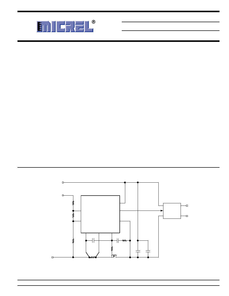
Typical Application
VDD
VEE
SENSE
GATE
DRAIN
/PWRGD
UV
OV
6
5
4
2
3
7
1
MIC2588-2BM
C
FDBK
C
GATE
R
FDBK
R3
12.4k
1%
Input Overvoltage = 71.2V
Input Undervoltage = 36.5V
(See "Functional Description" for more detail)
R2
11.8k
1%
R1
698k
1%
M1
R4
0.1
µ
F
DC-DC Converter
100
µ
F
/ON/OFF
IN+
+5V
OUT
5V
RETURN
≠48V
INPUT
(Long Pin)
≠48V
RETURN
(Short Pin)
≠48V
RETURN
(Long Pin)
IN≠
OUT+
OUT≠
R
SENSE
8
Features
∑ MIC2588:
Pin-for-pin functional equivalent to the
LT1640/LT1640A/LT4250
∑ Provides safe insertion and removal from live ≠48V
(nominal) backplanes
∑ Operates from ≠19V to ≠80V
∑ Electronic circuit breaker function
∑ Built-in 400
µ
s "nuisance-trip" delay (t
FLT
)
∑ Regulated maximum output current into faults
∑ Programmable inrush current limiting
∑ Fast response to short circuit conditions (< 1
µ
s)
∑ Programmable undervoltage and overvoltage lockouts
(MIC2588-xBM)
∑ Programmable UVLO hysteresis (MIC2594-xBM)
∑ Fault reporting:
Active-HIGH (-1BM) and Active-LOW
(-2BM) Power-Good signal output
Applications
∑ Central office switching
∑ ≠48V power distribution
∑ Distributed power systems
Micrel, Inc. ∑ 1849 Fortune Drive ∑ San Jose, CA 95131 ∑ USA ∑ tel + 1 (408) 944-0800 ∑ fax + 1 (408) 944-0970 ∑ http://www.micrel.com
MIC2588/MIC2594
Micrel
M9999-122303
2
December 2003
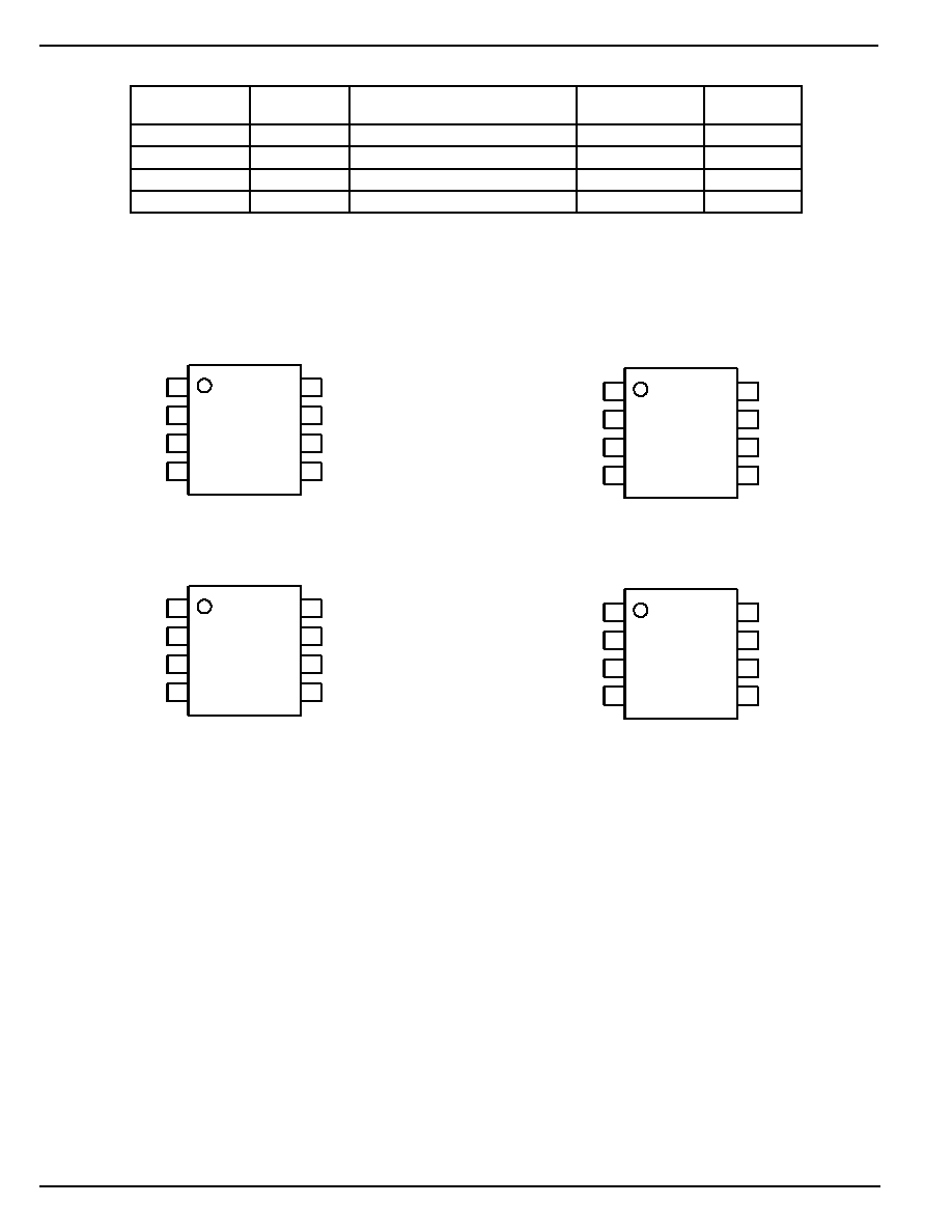
Pin Configuration
1
PWRGD
OV
UV
VEE
8
VDD
DRAIN
GATE
SENSE
7
6
5
2
3
4
8-Pin SOIC (M)
MIC2588-1BM
1
PWRGD
ON
OFF
VEE
8
VDD
DRAIN
GATE
SENSE
7
6
5
2
3
4
8-Pin SOIC (M)
MIC2594-1BM
Ordering Information
Part Number
PWRGD
Lockout Functions
Circuit Breaker
Package
Polarity
Function
MIC2588-1BM
Active-High
Undervoltage and Overvoltage
Latched Off
8-pin SOIC
MIC2588-2BM
Active-Low
Undervoltage and Overvoltage
Latched Off
8-pin SOIC
MIC2594-1BM
Active-High
Programmable UVLO Hysteresis
Latched Off
8-pin SOIC
MIC2594-2BM
Active-Low
Programmable UVLO Hysteresis
Latched Off
8-pin SOIC
1
/PWRGD
OV
UV
VEE
8
VDD
DRAIN
GATE
SENSE
7
6
5
2
3
4
8-Pin SOIC (M)
MIC2588-2BM
1
/PWRGD
ON
OFF
VEE
8
VDD
DRAIN
GATE
SENSE
7
6
5
2
3
4
8-Pin SOIC (M)
MIC2594-2BM

December 2003
3
M9999-122303
MIC2588/MIC2594
Micrel
Pin Description
Pin Number
Pin Name
Pin Function
PWRGD
Power-Good Output: Open-drain. Asserted when the voltage on the DRAIN
1
/PWRGD
pin (V
DRAIN
) is within V
PGTH
of VEE, indicating that the output voltage is
within proper specifications.
MIC25XX-1
MIC2588-1 and MIC2594-1: PWRGD will be high-impedance when
1
PWRGD
V
DRAIN
is less than V
PGTH
, and will pull-down to V
DRAIN
when V
DRAIN
is
Active-High
greater than V
PGTH
. Asserted State: Open-Drain.
MIC25XX-2
MIC2588-2 and MIC2594-2: /PWRGD will pull-down to V
DRAIN
when
1
/PWRGD
V
DRAIN
is less than V
PGTH,
and will be high impedance when V
DRAIN
is
Active-Low
greater than V
PGTH
. Asserted State: Active-Low.
OV
MIC2588: Overvoltage Threshold Input. When the voltage at the OV pin is
2
Threshold
greater than the V
OVH
threshold, the GATE pin is immediately pulled low by an
internal 100
µ
A current pull-down.
ON
MIC2594: Turn-On Threshold. At initial system power-up or after the device
2
Turn-On Threshold
has been shut off by the OFF pin, the voltage on the ON pin must exceed
the V
ONH
threshold in order for the MIC2594 to be enabled.
UV
MIC2588: Undervoltage Threshold Input. When the voltage at the UV pin is
3
Threshold
less than the V
UVL
threshold, the GATE pin is immediately pulled low by an
internal 100
µ
A current pull-down. The UV pin is also used to cycle the device
off and on to reset the circuit breaker. Taken together, the OV and UV pins
form a window comparator which defines the limits of V
EE
within which the
load may safely be powered.
OFF
MIC2594: Turn-Off Threshold. When the voltage at the OFF pin is less than
3
Turn-Off Threshold
the V
OFFL
threshold, the GATE pin is immediately pulled low by an internal
100
µ
A current pull-down. The OFF pin is also used to cycle the device off and
on to reset the circuit breaker. Taken together, the ON and OFF pins provide
programmable hysteresis for the turn-on command voltage.
4
VEE
Negative Supply Voltage Input.
5
SENSE
Circuit Breaker Sense Input: The current-limit threshold is set by connecting
a resistor between this pin and V
EE
. When the current-limit threshold of
IR = 50mV is exceeded for an internal delay t
FLT
(400
µ
s), the circuit breaker
is tripped and the GATE pin is immediately pulled low. Toggling UV or OV
will reset the circuit breaker. To disable the circuit breaker, externally
connect SENSE and VEE together.
6
GATE
Gate Drive Output: Connect to the gate of an external N-Channel MOSFET.
7
DRAIN
Drain Sense Input: Connect to the drain of an external N-Channel MOSFET.
8
VDD
Positive Supply Input.

MIC2588/MIC2594
Micrel
M9999-122303
4
December 2003
Absolute Maximum Ratings
(1)
(All voltages are referred to V
EE
)
Supply Voltage (V
DD
≠ V
EE
) ......................... ≠0.3V to 100V
DRAIN, PWRGD pins ................................... ≠0.3V to 100V
GATE pin ..................................................... ≠0.3V to 12.5V
SENSE, OV, UV, ON, OFF pins ....................... ≠0.3V to 6V
ESD Ratings
(3)
Human Body Model ................................................... 2kV
Soldering
Vapor Phase .......................... (60 sec.) +220
∞
C +5
±
0
∞
C
Infrared ................................... (15 sec.) +235
∞
C +5
±
0
∞
C
Operating Ratings
(2)
Supply Voltage (V
DD
≠ V
EE
) .......................... +19V to +80V
Ambient Temperature Range
(
T
A
) ............... ≠40
∞
C to 85
∞
C
Junction Temperature
(
T
J
) ........................................ 125
∞
C
Package Thermal Resistance
SOIC
(
JA
) ......................................................... 152
∞
C/W
DC Electrical Characteristics
(4)
V
DD
= 48V, V
EE
= 0V, T
A
= 25
∞
C, unless otherwise noted. Bold indicates specifications apply over the full operating temperature range of
≠40
∞
C to +85
∞
C.
Symbol
Parameter
Condition
Min
Typ
Max
Units
V
DD
≠ V
EE
Supply Voltage
19
80
I
DD
Supply Current
3
5
mA
V
TRIP
Circuit Breaker Trip Voltage
V
TRIP
= V
SENSE
≠ V
EE
40
50
60
mV
I
GATEON
GATE Pin Pull-up Current
V
GATE
= V
EE
to 8V
30
45
60
µ
A
19V
(V
DD
≠ V
EE
)
80V
I
GATEOFF
GATE Pin Sink Current
(V
SENSE
≠ V
EE
) = 100mV
100
230
mA
V
GATE
= 2V
V
GATE
GATE Drive Voltage, (V
GATE
≠ V
EE
)
15V
(V
DD
≠ V
EE
)
80V
9
10
11
V
I
SENSE
SENSE Pin Current
V
SENSE
= 50mV
0.2
µ
A
V
UVH
UV Pin High Threshold Voltage
Low-to-High Transition
1.213
1.243
1.272
V
V
UVL
UV Pin Low Threshold Voltage
High-to-Low Transition
1.198
1.223
1.247
V
V
UVHYS
UV Pin Hysteresis
20
mV
V
OVH
OV Pin High Threshold Voltage
Low-to-High Transition
1.198
1.223
1.247
V
V
OVL
OV Pin Low Threshold Voltage
High-to-Low Transition
1.165
1.203
1.232
V
V
OVHYS
OV Pin Hysteresis
20
mV
V
ONH
ANSI ON Pin High Threshold
Low-to-High Transition
1.198
1.223
1.247
V
Voltage
V
OFFH
ANSI OFF Pin Low Threshold
High-to-Low Transition
1.198
1.223
1.247
V
Voltage
I
CNTRL
Input Bias Current
V
UV
= 1.25V
0.5
µ
A
(OV, UV, ON, OFF Pins)
V
PGTH
Power-Good Threshold
High-to-Low Transition
1.1
1.26
1.40
V
(V
DRAIN
≠ V
EE
)
V
OLPG
PWRGD Output Voltage
V
OLPG
≠ V
DRAIN
(relative to voltage at the DRAIN pin) 0mA
I
PG(LOW)
1mA
MIC25XX-1
(V
DRAIN
≠ V
EE
) < V
PGTH
≠0.25
0.8
V
MIC25XX-2
(V
DRAIN
≠ V
EE
) > V
PGTH
≠0.25
0.8
V
I
LKG(PG)
PWRGD Output Leakage Current
V
PWRGD
= V
DD
= 80V
1
µ
A
Notes:
1. Exceeding the
"Absolute Maximum Ratings"
may damage the devices.
2. The devices are not guaranteed to function outside the specified operating conditions.
3. Devices are ESD sensitive. Handling precautions recommended. Human body model: 1.5k
in series with 100pF. Machine model: 200pF, no series
resistance.
4. Specification for packaged product only.

December 2003
5
M9999-122303
MIC2588/MIC2594
Micrel
AC Electrical Characteristics
(5)
Symbol
Parameter
Condition
Min
Typ
Max
Units
t
FLT
Built-in Overcurrent Nuisance Trip
Note 6
400
µ
s
Time Delay (Figure 1)
t
OCSENSE
Overcurrent Sense to GATE Low
V
SENSE
≠ V
EE
= 100mV
3.5
µ
s
(Figure 2)
t
OVPHL
OV to GATE Low (Figure 3)
Note 6
1
µ
s
t
OVPLH
OV to GATE High (Figure 3)
Note 6
1
µ
s
t
UVPHL
UV to GATE Low (Figure 4)
Note 6
1
µ
s
t
UVPLH
UV to GATE High (Figure 4)
Note 6
1
µ
s
t
PGL(1)
DRAIN High to PWRGD Output Low
R
PULLUP
= 100k
, C
LOAD
on PWRGD = 50pF
(6)
1
µ
s
(-1 Version parts only)
t
PGL(2)
DRAIN Low to /PWRGD Output Low
R
PULLUP
= 100k
, C
LOAD
on /PWRGD = 50pF
(6)
1
µ
s
(-2 Version parts only)
t
PGH(1)
DRAIN Low to PWRGD Output High
R
PULLUP
= 100k
, C
LOAD
on PWRGD = 50pF
(6)
2
µ
s
(-1 Version parts only)
t
PGH(2)
DRAIN High to /PWRGD Output High
R
PULLUP
= 100k
, C
LOAD
on /PWRGD = 50pF
(6)
2
µ
s
(-2 Version parts only)
Notes:
5. Specification for packaged product only.
6. Not 100% production tested. Parameters are guaranteed by design.
Test Circuit
[Section under construction]
MIC2588/MIC2594
Micrel
M9999-122303
6
December 2003
Typical Characteristics
[Section under construction]
0
1
2
3
4
5
6
7
8
9
10
0
2
4
6
8
10
XXX (X)
XXX (X)
MICx xxx
vs. xxx
0
1
2
3
4
5
6
7
8
9
10
0
2
4
6
8
10
XXX (X)
XXX (X)
MICx xxx
vs. xxx
0
1
2
3
4
5
6
7
8
9
10
0
2
4
6
8
10
XXX (X)
XXX (X)
MICx xxx
vs. xxx
0
1
2
3
4
5
6
7
8
9
10
0
2
4
6
8
10
XXX (X)
XXX (X)
MICx xxx
vs. xxx
0
1
2
3
4
5
6
7
8
9
10
0
2
4
6
8
10
XXX (X)
XXX (X)
MICx xxx
vs. xxx
0
1
2
3
4
5
6
7
8
9
10
0
2
4
6
8
10
XXX (X)
XXX (X)
MICx xxx
vs. xxx
0
1
2
3
4
5
6
7
8
9
10
0
2
4
6
8
10
XXX (X)
XXX (X)
MICx xxx
vs. xxx
0
1
2
3
4
5
6
7
8
9
10
0
2
4
6
8
10
XXX (X)
XXX (X)
MICx xxx
vs. xxx
0
1
2
3
4
5
6
7
8
9
10
0
2
4
6
8
10
XXX (X)
XXX (X)
MICx xxx
vs. xxx
0
1
2
3
4
5
6
7
8
9
10
0
2
4
6
8
10
XXX (X)
XXX (X)
MICx xxx
vs. xxx
0
1
2
3
4
5
6
7
8
9
10
0
2
4
6
8
10
XXX (X)
XXX (X)
MICx xxx
vs. xxx
0
1
2
3
4
5
6
7
8
9
10
0
2
4
6
8
10
XXX (X)
XXX (X)
MICx xxx
vs. xxx

December 2003
7
M9999-122303
MIC2588/MIC2594
Micrel
Timing Diagrams
I
LIMIT
I
LOAD
0A
V
DRAIN
V
GATE
(V
EE
+10V)
t < t
FLT
t
t
FLT
(at V
EE
)
(at V
EE
)
(at V
EE
)
OVERCURRENT
EVENT
Output OFF
(at V
DD
)
Load current is regulated
at I
LIMIT
= 50mV/R
SENSE
Reduction in V
DRAIN
to support
I
LIMIT
= 50mV/R
SENSE
Figure 1. Overcurrent Response
V
SENSE
- V
EE
100mV
1V
t
OCSENSE
V
GATE
Figure 2. SENSE to GATE LOW Timing Response
V
OV
1.223V
1V
1.203V
1V
t
OVPHL
V
GATE
t
OVPLH
Figure 3. Overvoltage Response
MIC2588/MIC2594
Micrel
M9999-122303
8
December 2003
V
UV
1.223V
1V
1.243V
1V
t
UVPHL
V
GATE
t
UVPLH
Figure 4. Undervoltage Response
V
DRAIN
MIC2588/94-1
MIC2588/94-2
V
PGTH
V
PGTH
V
EE
V
EE
V
PWRGD
-- V
DRAIN
= 0V
V
PWRGD
-- V
DRAIN
= 0V
t
PGH1
V
EE
V
EE
PWRGD
PWRGD not asserted
PWRGD not asserted
PWRGD asserted - High Impedance
t
PGL1
V
PGTH
V
PGTH
t
PGL2
t
PGH2
V
DRAIN
/PWRGD
Figure 5. DRAIN to Power-Good Response

December 2003
9
M9999-122303
MIC2588/MIC2594
Micrel
Functional Diagram
Logic +
Circuit
Breaker
Internal
PG
VEE
SENSE
VDD
+
≠
45
µ
A
50mV
V
PGTH
GATE
+
≠
V
TH(UV/OV)
UV
+
≠
OV
+
≠
V
DD1
V
EE
Internal VDD
and
Reference
Generator
Nuisance
Trip Filter
(400
µ
s)
Current
Limit
State
V
EE
EN
V
EE
denotes -2 option
V
EE
100
µ
A
/PWRGD
DRAIN
PWRGD
6V
Clamp
For Power Good circuitry only
V
REF1
V
DD1
V
DD1
MIC2588 Block Diagram

MIC2588/MIC2594
Micrel
M9999-122303
10
December 2003
Functional Description
Hot Swap Insertion
When circuit boards are inserted into systems carrying live
supply voltages ("hot swapped"), high inrush currents often
result due to the charging of bulk capacitance that resides
across the circuit board's supply pins. These current spikes
can cause the system's supply voltages to temporarily go out
of regulation, causing data loss or system lock-up. In more
extreme cases, the transients occurring during a hot swap
event may cause permanent damage to connectors or on-
board components.
The MIC2588 and the MIC2594 are designed to address
these issues by limiting the magnitude of the transient current
during hot swap events. This is achieved by controlling the
rate at which power is applied to the circuit board (di/dt and
dv/dt management). In addition, to inrush current control, the
MIC2588 and the MIC2594 incorporate input voltage super-
visory functions and current limiting, thereby providing robust
protection for both the system and the circuit board.
Start-Up Cycle
When the input voltage to the IC is between the overvoltage
and undervoltage thresholds (MIC2588) or is greater than
V
ON
(MIC2594), a start cycle is initiated. At this time, the
GATE pin of the IC applies a constant charging current
(I
GATEON
) to the gate of the external MOSFET (M1). C
FDBK
creates a Miller integrator out of the MOSFET circuit, which
limits the slew-rate of the voltage at the drain of M1. The drain
voltage rate-of-change (dv/dt) of M1 is:
dv M1
dt
I
C
≠
I
C
DRAIN
GATE(≠)
FDBK
GATEON
FDBK
(
)
=
=
where I
GATE(+)
= Gate Charging Current = I
GATEON
;
I
GATE(≠)
≠I
GATE(+)
, due to the extremely high
transconductance values of power MOSFETs; and
I
C
dv M1
dt
GATE(≠)
FDBK
DRAIN
=
◊
(
)
Relating the above to the maximum transient current into the
load capacitance to be charged upon hot swap or power-up
involves a simple extension of the same formula:
I
C
dv M1
dt
I
C
≠
I
C
| I
|
C
I
C
CHARGE
LOAD
DRAIN
CHARGE
LOAD
GATEON
FDBK
CHARGE
LOAD
GATEON
FDBK
=
◊
(
)
=
◊
=
◊
Transposing:
C
C
I
| I
|
FDBK
LOAD
GATEON
CHARGE
=
◊
(1)
C
GATE
and R
FDBK
prevent turn-on and hot swap current
surges which would otherwise be caused by (C
FDBK
+
C
D-G(M1)
) coupling turn-on transients from the drain to the
gate of M1. An appropriate value for C
GATE
may be deter-
mined using the formula for a capacitive voltage divider:
Maximum voltage on C
GATE
at turn-on must be less than
V
THRESHOLD
of M1:
1. For a standard 10V enhancement N-Channel
MOSFET, V
THRESHOLD
is about 4.25V.
2. Choose 3.5V as a safe maximum voltage to safely
avoid turn-on transients.
V
G-S(M1)
◊
[C
GATE
+ (C
FDBK
+ C
D-G(M1)
)]
= [(V
DD
≠ V
EE
(min))
◊
(C
FDBK
+ C
D-G(M1)
)]
V
G-S(M1)
◊
C
GATE
= [(V
DD
≠ V
EE
(min)) ≠ V
G-S(M1)
]
◊
(C
FDBK
+ C
D-G(M1)
)
C
C
C
V
≠ V (min) ≠ V
V
GATE
FDBK
D G(Q1)
DD
EE
G-S(M1)
G-S(M1)
=
+
(
)
◊
(
)
-
(2)
While the value for R
FDBK
is not critical, it should be chosen
to allow a maximum of several milliamperes to flow in the
gate-drain circuit of M1 during turn-on. While the final value
for R
FDBK
is determined empirically, initial values between
R
FDBK
= 15k
to 27k
for systems with a maximum value of
75V for (V
DD
≠ V
EE
(min)) are appropriate.
Resistor R4, in series with the MOSFETs gate, minimizes the
potential for parasitic high frequency oscillations from occur-
ring in M1. While the exact value of R4 is not critical,
commonly used values for R4 range from 10
to 33
.
For example, let us assume a hot swap controller is required
to maintain the inrush current into a 150
µ
F load capacitance
at 1.7A maximum, and that this circuit may operate from
supply voltages as high as (V
DD
≠ V
EE
) = 75V. The MOSFET
to be used with the MIC2588/94 is an IRF540NS 100V
D
2
PAK device which has a typical (C
D-G
) of 250pF.
Calculating a value for C
FBDK
using Equation 1 yields:
C
150 F
45 A
1.7A
3.97nF
FDBK
=
µ ◊
µ =
Good engineering practice suggests the use of the worst-
case parameter values for I
GATEON
from the
"DC Electrical
Characteristics"
section:
C
150 F
60 A
1.7A
5.3nF
FDBK
=
µ ◊ µ =
where the nearest standard 5% value is 5.6nF. Substituting
5.6nF into Equation 2 from above yields:
C
5.6nF
250pF
75V ≠ 3.5V
3.5V
0.12 F
GATE
=
+
(
)
◊
(
)
=
µ
Finally, choosing R4 = 10
and R
FDBK
= 20k
will yield a
suitable, initial design for prototyping.

December 2003
11
M9999-122303
MIC2588/MIC2594
Micrel
Power-Good (PWRGD or /PWRGD) Output
For the MIC2588-1 and the MIC2594-1, the Power-Good
output signal (PWRGD) will be high impedance when V
DRAIN
drops below V
PGTH
, and will pull down to V
DRAIN
when
V
DRAIN
is above V
PGTH
. For the MIC2588-2 and the
MIC2594-2, /PWRGD will pull down to the potential of the
V
DRAIN
pin when V
DRAIN
drops below V
PGTH
, and will be high
impedance when V
DRAIN
is above V
PGTH
. Hence, the -1 parts
have an active-high PWRGD signal and the -2 parts have an
active-low /PWRGD output. Either PWRGD or /PWRGD may
be used as an enable signal for one or more subsequent
DC/DC converter modules or for other system uses as
desired. When used as an enable signal, the time necessary
for the PWRGD (or /PWRGD) signal to pull-up (when in high
impedance state) will depend upon the load (RC) that is
present on this output.
Circuit Breaker Function
The MIC2588 and the MIC2594 employ an electronic circuit
breaker that protects the MOSFET and other system compo-
nents against faults such as short circuits. The current limit
threshold is set via an external resistor, R
SENSE
, connected
between the V
EE
and SENSE pins. An internal 400
µ
s timer
limits the length of time (t
FLT
) for which the circuit can draw
current in excess of its programmed threshold before the
circuit breaker is tripped. This short delay prevents nuisance
tripping of the circuit breaker due to system transients while
providing rapid protection against large-scale transient faults.
Whenever the voltage across R
SENSE
exceeds 50mV, two
things happen:
1. A constant-current regulation loop is engaged de-
signed to hold the voltage across R
SENSE
equal to
50mV. This protects both the load and the MIC2588
circuit from excessively high currents. This loop will
engage in less than 1
µ
s from the time at which the
overvoltage condition on R
SENSE
occurs.
2. The internal 400
µ
s timer is started. If the 400
µ
s
timeout period is exceeded, the circuit breaker trips
and the GATE pin is immediately pulled low by an
internal current pull-down. This operation turns off
the MOSFET quickly and disconnects the input from
the load.
Current Sensing
As mentioned before, the MIC2588 and the MIC2594 employ
an external low-value resistor in series with the source of the
external MOSFET to measure the current flowing into the
load. The V
EE
connection to the IC from the negative supply
is also one input to the part's internal current sensing circuits
and the SENSE input is the other input.
Sense Resistor Selection
The sense resistor is nominally valued at:
R
(nom)
V
(typ)
I
(nom)
SENSE
TRIP
HOT_SWAP
=
where V
TRIP
(typ) is the nominal circuit breaker threshold
voltage (= 50mV) and I
HOT_SWAP
(nom) is the nominal hot
swap load current level to trip the internal circuit breaker in the
application.
To accommodate worst-case tolerances in the sense resistor
(for a
±
1% initial tolerance, allow
±
3% tolerance for variations
over time and temperature) and circuit breaker threshold
voltages, a slightly more detailed calculation must be used to
determine the minimum and maximum hot swap load
currents.
As the MIC2588/94's minimum current limit threshold voltage
is 40mV, the minimum hot swap load current is determined
where the sense resistor is 3% high:
I
(min)
40mV
1.03 R
(nom)
38.8mV
R
(nom)
HOT_SWAP
SENSE
SENSE
=
◊
(
)
=
Keep in mind that the minimum hot swap load current should
be greater than the application circuit's upper steady-state
load current boundary. Once the lower value of R
SENSE
has
been calculated, it is good practice to check the maximum hot
swap load current (I
HOT_SWAP
(max)) which the circuit may let
pass in the case of tolerance build-up in the opposite direc-
tion. Here, the worst-case maximum is found using a
V
TRIP
(max) of 60mV and a sense resistor, 3% low in value:
I
(max)
60mV
0.97 R
(nom)
61.9mV
R
(nom)
HOT_SWAP
SENSE
SENSE
=
◊
(
)
=
In this case, the application circuit must be sturdy enough to
operate over a ~1.6-to-1 range in hot swap load currents. For
example, if an MIC2594 circuit must pass a minimum hot
swap load current of 4A without nuisance trips, R
SENSE
should be set to
38.8mV
4A
9.7m
=
, and the nearest 1%
standard value is 9.76m
. At the other tolerance extremes,
I
HOT_SWAP
(max) for the circuit in question is then simply
I
(max)
61.9mV
9.76m
6.3A
HOT_SWAP
=
=
With a knowledge of the application circuit's maximum hot
swap load current, the power dissipation rating of the sense
resistor can be determined using P = I
2
◊
R. Here, the I is
I
HOT_SWAP
(max) = 6.3A and the R is R
SENSE
(min)
=
(0.97)(R
SENSE
(nom)) = 9.47m
. Thus, the sense resistor's
maximum power dissipation is:
P
MAX
= (6.3A)
2
◊
(9.47m
) = 0.376W
A 0.5
sense resistor is a good choice in this application.
Undervoltage/Overvoltage Detection--MIC2588
The MIC2588 has "UV" and "OV" input pins. These pins can be
used to detect input supply rail undervoltage and overvoltage
conditions. Undervoltage lockout prevents energizing the load
until the supply input is stable and within tolerance. In a similar
fashion, overvoltage turn-off prevents damage to sensitive
circuit components should the input voltage exceed normal
operational limits. Each of these pins is internally connected to
an analog comparator with 20mV of hysteresis. When the UV
pin falls below its V
UVL
threshold or the OV pin is above its V
OVH
threshold, the GATE pin is immediately pulled low. The GATE
pin will be held low until UV exceeds its V
UVH
threshold or OV
drops below its V
OVL
threshold. The UV and OV circuit's
threshold trip points are programmed using the resistor divider

MIC2588/MIC2594
Micrel
M9999-122303
12
December 2003
R1, R2, and R3 as shown in the
"Typical Application."
The
equations to set the trip points are shown below. For the
following example, the circuit's UV threshold is set to V
UV
= 37V
and the OV threshold is placed at V
OV
= 72V, values commonly
used in Central Office power distribution applications.
V
V
(typ)
R1+ R2 + R3
R2 + R3
V
V
(typ)
R1+ R2 + R3
R3
UV
UVL
OV
OVH
=
◊
(
)
(
)
=
◊
(
)
Given V
UV
, V
OV
, and any one resistor value, the remaining
two resistor values can be found. A suggested value for R3
is that which will provide approximately 100
µ
A of current
through the voltage divider chain at V
DD
= V
UV
. This yields the
following as a starting point:
R3
V
(typ)
100 A
12.23k
OVH
=
µ
=
The closest standard 1% value for R3 = 12.4k
. Solving for
R2 and R1 yields:
R2
R3
V
V
≠ 1
R2
12.4k
72V
37V
≠ 1
R2
11.729k
OV
UV
=
◊
=
◊
=
The closest standard 1% value for R2 = 11.8k
. Next, the
value for R1 is calculated:
R1 R3
V
≠ 1.223V
1.223V
≠ R2
R1 12.4k
72V ≠ 1.223V
1.223V
≠ R2
R1 705.808k
OV
=
◊
=
◊
=
The closest standard 1% value for R1 = 698k
.
Using standard 1% resistor values, the circuit's nominal
UV and OV thresholds are:
V
UV
= 36.5V
V
OV
= 71.2V
Programmable UVLO Hysteresis--MIC2594
The MIC2594 has user-programmable hysteresis by means of
the ON and OFF pins. This allows setting the part to turn on at
a voltage V1, and not turn off until a second voltage V2, where
V2 < V1. This can significantly simplify dealing with source
impedances in the supply bus while at the same time increasing
the amount of available operating time from a loosely regulated
power supply (for example, a battery supply). Similarly to the
MIC2588, each of these pins is internally connected to an
analog comparator with 20mV of hysteresis. The MIC2594
holds the output off until the voltage at the ON pin exceeds its
V
ONH
threshold value given in the
"Electrical Characteristics"
table. Once the output has been enabled by the ON pin, it will
remain on until the voltage at the OFF pin falls below its V
OFFL
threshold value, or the part turns off due to a fault. Should either
event occur, the GATE pin is immediately pulled low and will
remain low until the ON pin once again exceeds its V
ONH
threshold. The circuit's turn-on and turn-off points are set using
the resistor divider R1, R2, and R3 as shown in the
"Typical
Application."
The equations to establish the trip points are
shown below. In the following example, the circuit's ON thresh-
old is set to V
ON
=
40V and the circuit's OFF threshold is V
OFF
= 35V.
V
= V
(typ)
R1 R2 R3
R3
V
= V
(typ)
R1 R2 R3
R2 R3
ON
ONH
OFF
OFFL
◊
+
+
(
)
◊
+
+
(
)
+
(
)
Given V
OFF
, V
ON
, and any one resistor value, the remaining
two resistor values can be readily found. A suggested value
for R3 is that which will provide approximately 100
µ
A of
current through the voltage divider chain at V
DD
= V
OFF
. This
yields the following as a starting point:
R3 =
V
(typ)
100 A
12.23k
OFFL
µ
=
The closest standard 1% value for R3 = 12.4k
.
Then, solving for R2 and R1 yields:
R2 = R3
V
V
≠ 1
R2 = 12.4k
40V
35V
≠ 1
R2 = 1.771k
ON
OFF
◊
◊
The closest standard 1% value for R2 = 1.78k
.
R1= R3
V
≠ 1.223V
1.223V
≠ R2
R1= 12.4k
40V ≠ 1.223V
1.223V
≠ R2
R1= 391.380k
ON
◊
(
)
◊
(
)
The closest standard 1% value for R1 = 392k
.
Using standard 1% resistor values, the circuit's nominal
ON and OFF thresholds are:
V
ON
= 40.1V
V
OFF
= 35V
December 2003
13
M9999-122303
MIC2588/MIC2594
Micrel
Applications Information
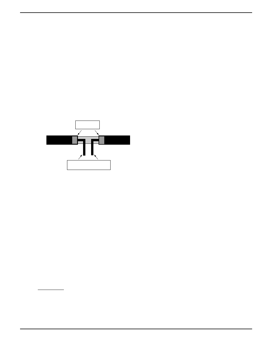
4-Wire Kelvin Sensing
Because of the low value typically required for the sense
resistor, special care must be used to measure accurately the
voltage drop across it. Specifically, the measurement tech-
nique across each R
SENSE
must employ 4-wire Kelvin sens-
ing. This is simply a means of making sure that any voltage
drops in the power traces connecting to the resistors are not
picked up by the signal conductors measuring the voltages
across the sense resistors.
Figure 6 illustrates how to implement 4-wire Kelvin sensing.
As the figure shows, all the high current in the circuit (from V
EE
through R
SENSE
, and then to the source of the output MOSFET)
flows directly through the power PCB traces and R
SENSE
. The
voltage drop resulting across R
SENSE
is sampled in such a
way that the high currents through the power traces will not
introduce any parasitic voltage drops in the sense leads. It is
recommended to connect the hot swap controller's sense
leads directly to the sense resistor's metalized contact pads.
R
SENSE
Power Trace
From V
EE
PCB Track Width:
0.03" per Ampere
using 1oz Cu
Power Trace
To MOSFET Source
Signal Trace
to MIC2588/94 V
EE
Pin
Signal Trace
to MIC2588/94 SENSE Pin
Note: Each SENSE lead trace shall be
balanced for best performance -- equal
length/equal aspect ratio.
R
SENSE
metalized
contact pads
Figure 6. 4-Wire Kelvin Sense Connections for R
SENSE
Protection Against Voltage Transients
In many telecom applications, it is very common for circuit
boards to encounter large-scale supply-voltage transients in
backplane environments. Because backplanes present a
complex impedance environment, these transients can be as
high as 2.5 times steady-state levels, or 120V in worst-case
situations. In addition, a sudden load dump anywhere on the
circuit card can generate a very high voltage spike at the drain
of the output MOSFET which, in turn, will appear at the
DRAIN pin of the MIC2588/MIC2594. In both cases, it is good
engineering practice to include protective measures to avoid
damaging sensitive ICs or the hot swap controller from these
large-scale transients. Two typical scenarios in which large-
scale transients occur are described below:
1. An output current load dump with no bypass (charge
bucket or bulk) capacitance to V
EE
. For example,
if L
LOAD
= 5
µ
H, V
IN
= 56V and t
OFF
= 0.7
µ
s, the
resulting peak short-circuit current prior to the
MOSFET turning off would reach:
55V
0.7 s
5 H
7.7A
◊
µ
(
)
µ
=
If there is no other path for this current to take when
the MOSFET turns off, it will avalanche the drain-
source junction of the MOSFET. Since the total
energy represented is small relative to the sturdi-
ness of modern power MOSFETs, it's unlikely that
this will damage the transistor. However, the actual
avalanche voltage is unknown; all that can be
guaranteed is that it will be greater than the V
BD(D-
S)
of the MOSFET. The drain of the transistor is
connected to the DRAIN pin of the MIC2588/94,
and the resulting transient does have enough
voltage and energy and can damage this, or any,
high-voltage hot swap controller.
2. If the load's bypass capacitance (for example, the
input filter capacitors for a set of DC-DC converter
modules) are on a board from which the board with
the MIC2589/MIC2595 and the MOSFET can be
unplugged, the same type of inductive transient
damage can occur to the MIC2588/MIC2594.
Protecting the controller and the power MOSFET from dam-
age against these large-scale transients can take the forms
shown in Figure 7. It is not mandatory that these techniques
are used--the application environment will dictate suitability.
As protection against sudden on-card load dumps at the
DRAIN pin of the controller, a 2.2
µ
F or larger capacitor
directly from DRAIN to V
EE
of the controller can be used to
serve as a charge reservoir. Alternatively, a 68V, 1W, 5%
Zener diode clamp can be installed in a similar fashion. Note
that the clamp diode's cathode is connected to the DRAIN pin
as shown in Figure 7. To protect the hot swap controller from
large-scale transients at the card input, a 100V clamp diode
(an SMAT70A or equivalent) can be used. In either case, the
lead lengths should be short and the layout compact to
prevent unwanted transients in the protection circuit.
[Circuit drawing under construction]
Figure 7. Using Large-Scale Transient Protection
Devices Around the MIC2588/94
Power buss inductance could easily result in localized high-
voltage transients during a turn-off event. The potential for
overstressing the part in such a case should be kept in check
with a suitable input capacitor and/or transient clamping
diode.
Power MOSFET Selection
[Section under construction]
Power MOSFET Operating Voltage Requirements
[Section under construction]
Power MOSFET Steady-State Thermal Issues
[Section under construction]
Power MOSFET Transient Thermal Issues
[Section under construction]
PCB Layout Considerations
[Section under construction]
Power MOSFET and Sense Resistor Vendors
[Section under construction]
MIC2588/MIC2594
Micrel
M9999-122303
14
December 2003
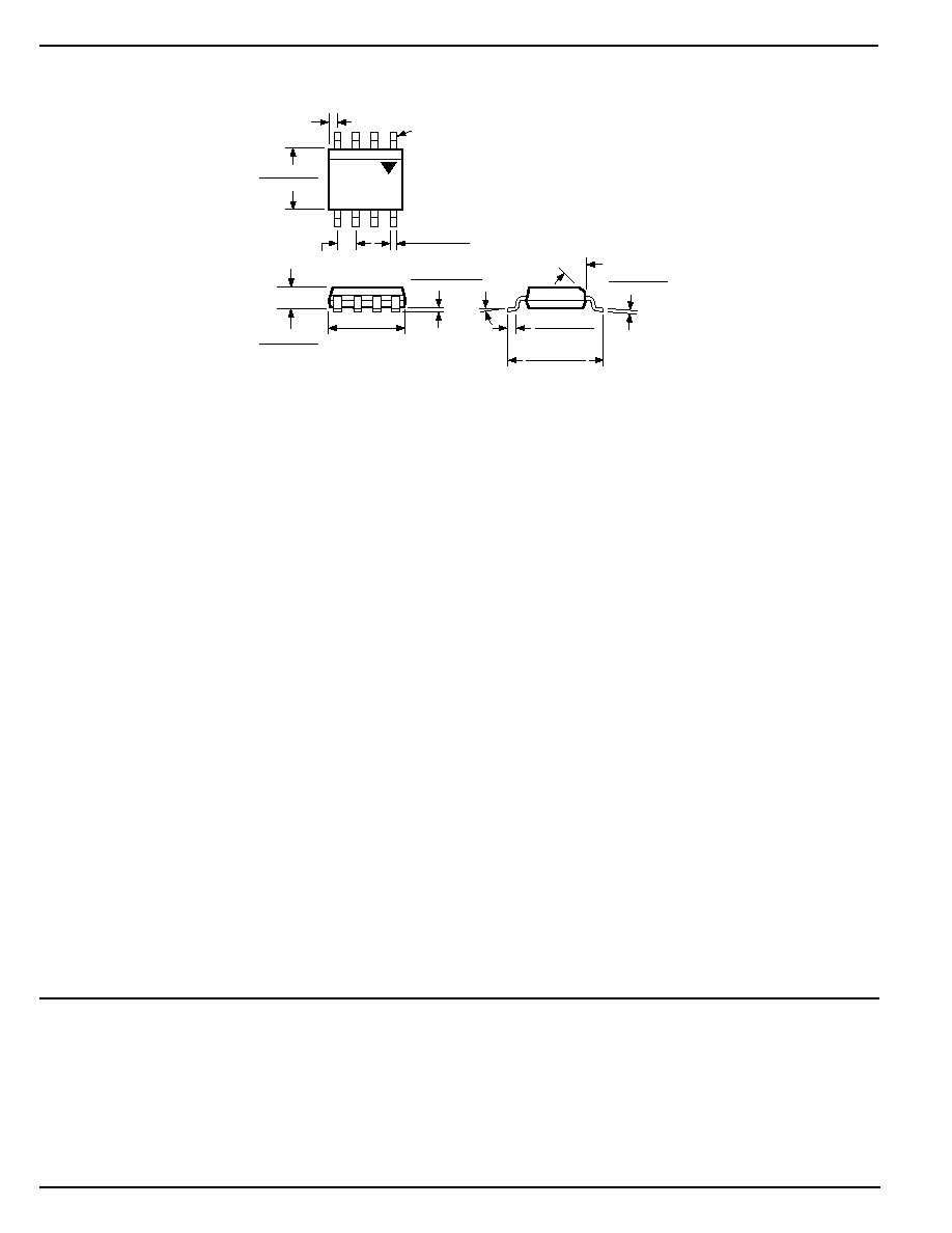
Package Information
45
∞
0
∞
≠8
∞
0.244 (6.20)
0.228 (5.79)
0.197 (5.0)
0.189 (4.8)
SEATING
PLANE
0.026 (0.65)
MAX
)
0.010 (0.25)
0.007 (0.18)
0.064 (1.63)
0.045 (1.14)
0.0098 (0.249)
0.0040 (0.102)
0.020 (0.51)
0.013 (0.33)
0.157 (3.99)
0.150 (3.81)
0.050 (1.27)
TYP
PIN 1
DIMENSIONS:
INCHES (MM)
0.050 (1.27)
0.016 (0.40)
8-Pin SOIC (M)
MICREL, INC.
1849 FORTUNE DRIVE
SAN JOSE, CA 95131
USA
TEL
+ 1 (408) 944-0800
FAX
+ 1 (408) 944-0970
WEB
http://www.micrel.com
The information furnished by Micrel in this data sheet is believed to be accurate and reliable. However, no responsibility is assumed by Micrel for its use.
Micrel reserves the right to change circuitry and specifications at any time without notification to the customer.
Micrel Products are not designed or authorized for use as components in life support appliances, devices or systems where malfunction of a product can
reasonably be expected to result in personal injury. Life support devices or systems are devices or systems that (a) are intended for surgical implant into
the body or (b) support or sustain life, and whose failure to perform can be reasonably expected to result in a significant injury to the user. A Purchaser's
use or sale of Micrel Products for use in life support appliances, devices or systems is at Purchaser's own risk and Purchaser agrees to fully indemnify
Micrel for any damages resulting from such use or sale.
© 2003 Micrel, Incorporated.