 | –≠–ª–µ–∫—Ç—Ä–æ–Ω–Ω—ã–π –∫–æ–º–ø–æ–Ω–µ–Ω—Ç: MIC2589 | –°–∫–∞—á–∞—Ç—å:  PDF PDF  ZIP ZIP |
March 2004
1
M9999-031504
MIC2589/2595
Micrel
MIC2589/MIC2595
Single-Channel, Negative High-Voltage Hot
Swap Power Controllers/Sequencers
General Description
The MIC2589 and MIC2595 are single-channel, negative-
voltage hot swap controllers designed to address the need for
safe insertion and removal of circuit boards into "live" system
backplanes, while using few external components. The
MIC2589/89R and the MIC2595/95R are each available in
14-pin SOIC packaging and work in conjunction with an
external N-Channel MOSFET for which the gate drive is
controlled to provide inrush current limiting and output volt-
age slew-rate control. Overcurrent fault protection is also
provided for which the overcurrent threshold and the
overcurrent duration are programmable. Very fast fault re-
sponse is provided to ensure that system power supplies
maintain regulation even during output short circuits. This
family offers two responses to a circuit breaker fault condition:
the MIC2589 and MIC2595 latch the circuit breaker's output
off if the overcurrent threshold interval is exceeded while the
MIC2589R and MIC2595R automatically attempt to restart at
a fixed duty cycle after a current limit fault. A primary
Power-Good signal and two secondary (delayed and stag-
gered) Power-Good signals are provided to indicate that the
output voltage of the inrush current limiter is within its valid
operating range. These signals can be used to perform an all-
at-once or a sequenced enabling of one or more DC-DC
power modules.
All support documentation can be found on Micrel's web
site at www.micrel.com.
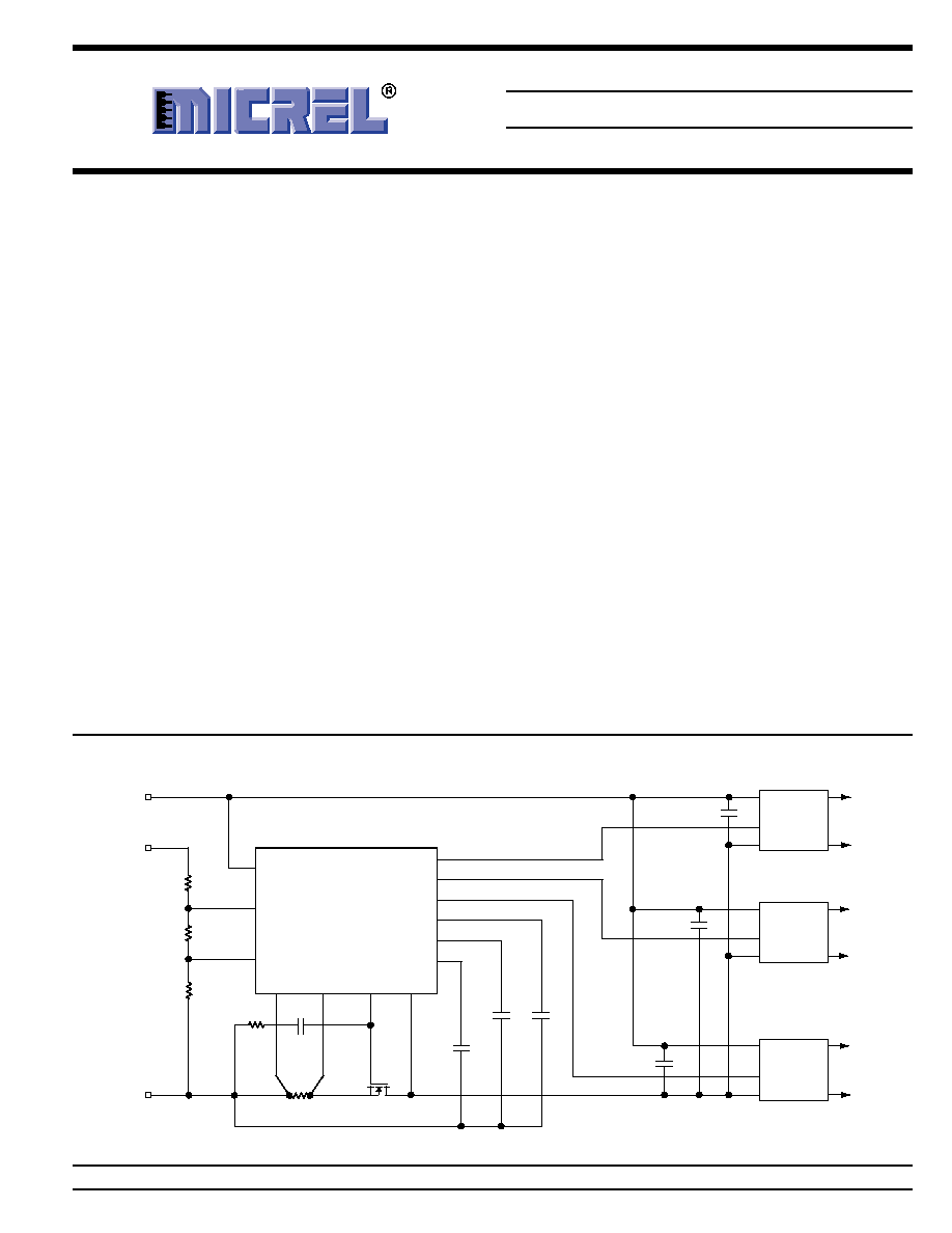
Typical Application
VDD
VEE
SENSE
GATE
DRAIN
CFILTER
UV
OV
10
9
7
4
3
14
11
5
MIC2589-1BM
MIC2589R-1BM
CNLD
6
PWRGD1
1
PWRGD2
12
PWRGD3
13
PGTIMER
2
C
GATE
M1
R4
0
C
PG
C
FILTER
C
NLD
≠48V
INPUT
(Long Pin)
≠48V
RETURN
(Short Pin)
≠48V
RETURN
(Long Pin)
R
SENSE
DC-DC Converter
100
µ
F
/ON/OFF
IN+
+3.3V
+3.3V
RETURN
IN≠
OUT
GND
DC-DC Converter
100
µ
F
/ON/OFF
IN+
+5V
+5V
RETURN
IN≠
OUT
GND
DC-DC Converter
100
µ
F
/ON/OFF
IN+
+2.5V
+2.5V
RETURN
IN≠
OUT
GND
R3
12.4k
1%
Input Overvoltage = 71.2V
Input Undervoltage = 36.5V
(See "Functional Description" for more detail)
R2
11.8k
1%
R1
698k
1%
Features
∑ Provides safe insertion and removal from live
≠48V (nominal) backplanes
∑ Operates from ≠19V to ≠80V
∑ Fast responding circuit breaker (<1
µ
s) to short circuit
conditions
∑ User-programmable overcurrent detector response time
∑ Electronic circuit breaker function:
Output latch OFF (MIC2589/95) or
Output auto-retry (MIC2589R/95R)
∑ Active current regulation precisely controls inrush
currents
∑ Regulated maximum output currents into faults
∑ Programmable undervoltage and overvoltage lockouts
(MIC2589/89R)
∑ Programmable UVLO hysteresis (MIC2595/95R)
∑ Staggered `Power-Good' outputs provide load
sequencing
∑ Fault reporting:
Active-HIGH (MIC25XX-1) and Active-LOW
(MIC25XX-2) Power-Good signal output
Applications
∑ Central office switching
∑ ≠48V power distribution
∑ Distributed power systems
Micrel, Inc. ∑ 1849 Fortune Drive ∑ San Jose, CA 95131 ∑ USA ∑ tel + 1 (408) 944-0800 ∑ fax + 1 (408) 944-0970 ∑ http://www.micrel.com

MIC2589/2595
Micrel
M9999-031504
2
March 2004
Ordering Information
PWRGD
Circuit Breaker
Part Number
Polarity
Input Voltage Monitor Pins
Function
Package
MIC2589-1BM
Active-High
Programmable UVLO & OVLO
Latched Off
14-pin SOIC
MIC2589-2BM
Active-Low
Programmable UVLO & OVLO
Latched Off
14-pin SOIC
MIC2589R-1BM
Active-High
Programmable UVLO & OVLO
Auto-Retry
14-pin SOIC
MIC2589R-2BM
Active-Low
Programmable UVLO & OVLO
Auto-Retry
14-pin SOIC
MIC2595-1BM
Active-High
Programmable UVLO Hysteresis
Latched Off
14-pin SOIC
MIC2595-2BM
Active-Low
Programmable UVLO Hysteresis
Latched Off
14-pin SOIC
MIC2595R-1BM
Active-High
Programmable UVLO Hysteresis
Auto-Retry
14 pin SOIC
MIC2595R-2BM
Active-Low
Programmable UVLO Hysteresis
Auto-Retry
14-pin SOIC
Pin Configuration
1
PWRGD1
PGTIMER
UV
OV
CFILTER
CNLD
VEE
14 VDD
PWRGD3
PWRGD2
DRAIN
GATE
SENSE
NC
13
12
11
10
9
8
2
3
4
5
6
7
14-Pin SOIC (M)
MIC2589-1BM
MIC2589R-1BM
1
PWRGD1
PGTIMER
OFF
ON
CFILTER
CNLD
VEE
14 VDD
PWRGD3
PWRGD2
DRAIN
GATE
SENSE
NC
13
12
11
10
9
8
2
3
4
5
6
7
14-Pin SOIC (M)
MIC2595-1BM
MIC2595R-1BM
1
/PWRGD1
PGTIMER
UV
OV
CFILTER
CNLD
VEE
14 VDD
/PWRGD3
/PWRGD2
DRAIN
GATE
SENSE
NC
13
12
11
10
9
8
2
3
4
5
6
7
14-Pin SOIC (M)
MIC2589-2BM
MIC2589R-2BM
1
/PWRGD1
PGTIMER
OFF
ON
CFILTER
CNLD
VEE
14 VDD
/PWRGD3
/PWRGD2
DRAIN
GATE
SENSE
NC
13
12
11
10
9
8
2
3
4
5
6
7
14-Pin SOIC (M)
MIC2595-2BM
MIC2595R-2BM

March 2004
3
M9999-031504
MIC2589/2595
Micrel
Pin Description
Pin Number
Pin Name
Pin Function
PWRGD1
Power-Good Output 1: Asserted when the voltage on the DRAIN pin
(MIC25XX-1)
(V
DRAIN
) is within V
PGTH
of VEE, indicating that the output voltage is within
Active-High
proper specifications. For the MIC2589-1 and MIC2985-1, PWRGD1 will be
1
high impedance when V
DRAIN
is less than V
PGTH
, and will pull-down to
/PWRGD1
V
DRAIN
when V
DRAIN
is greater than V
PGTH
. For the MIC2589-2 and
(MIC25XX-2)
MIC2595-2, /PWRGD1 will pull-down to V
DRAIN
when V
DRAIN
is less than
Active-Low
V
PGTH
, and will be high-impedance when V
DRAIN
is greater than V
PGTH
.
2
PGTIMER
A capacitor connected from this pin to VEE sets the time interval between
assertions of PWRGD2 (or /PWRGD2) and PWRGD3 (or /PWRGD3)
relative to PWRGD1 (or /PWRGD1). See the "Functional Description" for
further detail.
3
UV
MIC2589 and MIC2589R: Undervoltage Threshold Input. When the voltage
Threshold
at the UV pin is less than the V
UVL
threshold, the GATE pin is immediately
pulled low by an internal 100
µ
A current pull-down. The UV pin is also used
to cycle the device off and on to reset the circuit breaker. Taken together,
the OV and UV pins form a window comparator which define the limits of
V
EE
within which the load may safely be powered.
3
OFF
MIC2595 and MIC2595R: Turn-Off Threshold. When the voltage at the OFF
(Turn-Off Threshold)
pin is less than the V
OFFL
threshold, the GATE pin is immediately pulled
low by an internal 100
µ
A current pull-down. The OFF pin is also used to cycle
the device off and on to reset the circuit breaker. Taken together, the ON
and OFF pins provide programmable hysteresis for the MIC2595 to be
enabled.
4
OV
MIC2589 and MIC2589R: Overvoltage Threshold Input. When the voltage
Threshold
at the OV pin is greater than the V
OVH
threshold, the GATE pin is immediately
pulled low by an internal 100
µ
A current pull-down.
4
ON
MIC2595 and MIC2595R: Turn-On Threshold. At initial system power-up or
(Turn-On Threshold)
after the part has been shut off by the OFF pin, the voltage on the ON pin
must be above the V
ONH
threshold in order for the MIC2595 to be enabled.
5
CFILTER
Current Limit Response Timer: A capacitor connected between this pin and
VEE provides filtering against nuisance tripping of the circuit breaker by
setting a time delay, t
FLT
, for which an overcurrent event must last prior to
signaling a fault condition and latching the output off. The minimum time for
t
FLT
will be the time it takes for the output (capacitance) to charge to V
EE
during start-up. This pin is held to VEE with a 3
µ
A current pull-down when
no current limit condition exists. See the "Functional Description" for further
details.
6
CNLD
No-Load Detect Timer: A capacitor between this pin and VEE sets the
interval, t
NLD
, for which the current through the external MOSFET can drop
below 10% of full-scale current limit before the circuit breaker is tripped.
Tying this pin to V
EE
will disable this function. This pin is held to VEE by an
internal NMOS when there is no undercurrent condition.
7
VEE
Negative Supply Voltage Input.
8
NC
No Internal Connection.
9
SENSE
Circuit Breaker Sense Input: A resistor between this pin and VEE sets the
current limit trip point for the circuit. When the current limit threshold of IR =
50mV is exceeded for t
FLT
, the circuit breaker is tripped and the GATE pin is
immediately pulled low. Toggling UV or OV will reset the circuit breaker. To
disable the circuit breaker, externally tie SENSE and VEE can be connected
together.
10
GATE
Gate Drive Output: Connects to the Gate of an N-Channel MOSFET.
11
DRAIN
Drain Sense Input: Connects to the Drain of an N-Channel MOSFET.

MIC2589/2595
Micrel
M9999-031504
4
March 2004
Pin Number
Pin Name
Pin Function
12
PWRGD2
Power-Good Output 2: Asserted when the following is true: (PWRGD1 =
(MIC2589-1)
Asserted) AND (Time after Assertion of PWRGD1 = Time PWRGD2, as
(MIC2595-1)
programmed by the capacitor on PGTIMER). Once PWRGD1 is asserted,
the PGTIMER pin begins to change and PWRGD2 will assert when
PGTIMER crosses the PWRGD2 threshold (V
THRESH(PG2)
= 0.63V, typical).
Also see PWRGD1 and PGTIMER pin descriptions.
12
/PWRGD2
/Power-Good Output 2: Asserted when the following is true: (/PWRGD1 =
(MIC2589-2)
Asserted) AND (Time after Assertion of /PWRGD1 = Time /PWRGD2, as
(MIC2595-2)
programmed by the capacitor on PGTIMER). Once /PWRGD1 is asserted, the
PGTIMER pin begins to change and /PWRGD2 will assert when PGTIMER
crosses the /PWRGD2 threshold (V
THRESH(PG2)
= 0.63V, typical). Also see
/PWRGD1 and PGTIMER pin descriptions.
13
PWRGD3
Power-Good Output 3: Asserted when the following is true: (PWRGD1 =
(MIC2589-1)
Asserted) AND (Time after Assertion of PWRGD1 = Time PWRGD3, as
(MIC2595-1)
programmed by the capacitor on PGTIMER). Once PWRGD1 is asserted,
the PGTIMER pin begins to change and PWRGD3 will assert when
PGTIMER crosses the PWRGD3 threshold (V
THRESH(PG3)
= 1.15V, typical).
Also see PWRGD1 and PGTIMER pin descriptions.
13
/PWRGD3
/Power-Good Output 3: Open Collector. Asserted when the following is true:
(MIC2589-2)
(/PWRGD1 = Asserted) AND (Time after Assertion of /PWRGD1 = Time
(MIC2595-2)
/PWRGD3, as programmed by the capacitor on PGTIMER). Once /PWRGD1
is asserted, the PGTIMER pin begins to change and /PWRGD3 will assert
when PGTIMER crosses the /PWRGD3 threshold (V
THRESH(PG3)
= 1.15V,
typical). Also see /PWRGD1 and PGTIMER pin descriptions.
14
VDD
Positive Supply Input.

March 2004
5
M9999-031504
MIC2589/2595
Micrel
Absolute Maximum Ratings
(1)
(All voltages are referred to V
EE
)
Supply Voltage (V
DD
≠ V
EE
) ......................... ≠0.3V to 100V
DRAIN, PWRGD pins ................................... ≠0.3V to 100V
GATE pin ..................................................... ≠0.3V to 12.5V
SENSE, OV, UV, ON, OFF pins ....................... ≠0.3V to 6V
ESD Ratings
(3) ..............................................................................
2kV
Soldering
Vapor Phase .......................... (60 sec.) +220
∞
C +5
±
0
∞
C
Infrared ................................... (15 sec.) +235
∞
C +5
±
0
∞
C
Operating Ratings
(2)
Supply Voltage (V
DD
-V
EE
) ............................. +19V to +80V
Ambient Temperature Range (T
A
) ............... ≠40
∞
C to 85
∞
C
Junction Temperature (T
J
) ........................................ 125
∞
C
Package Thermal Resistance
SOIC
(
JA
) ......................................................... 120
∞
C/W
DC Electrical Characteristics
(4)
V
DD
= 48V, V
EE
= 0V, T
A
= 25
∞
C, unless otherwise noted. Bold indicates specifications apply over the full operating temperature range of ≠40
∞
C to 85
∞
C.
Symbol
Parameter
Condition
Min
Typ
Max
Units
V
DD
≠ V
EE
Supply Voltage
19
80
I
DD
Supply Current
4
6
mA
V
TRIP
Circuit Breaker Trip Voltage
V
TRIP
= V
SENSE
≠ V
EE
40
50
60
mV
I
NLDTH
No-Load Detect Threshold
% of full-scale current limit
I
OUT
decreasing
20
%
I
OUT
increasing
22
%
I
NLDHYS
No-Load Detect Threshold Hysteresis
% of full-scale current limit
2
%
V
CNLD
No-Load Detect Timer High Threshold
1.17
1.24
1.33
V
Voltage
I
CNLD
No-Load Detect Timer Capacitor
Note 5
10
25
40
µ
A
Charge Current
V
GATE
GATE Drive Voltage, (V
GATE
≠ V
EE
)
15V
(V
DD
≠ V
EE
)
80V
9
10
11
V
I
GATEON
GATE Pin Pull-Up Current
V
GATE
= V
EE
to 8V
30
45
60
µ
A
19V
(V
DD
≠ V
EE
)
80V
I
SENSE
SENSE Pin Current
V
SENSE
= 50mV
0.2
µ
A
I
GATEOFF
GATE Pin Sink Current
(V
SENSE
≠ V
EE
) = 100mV
100
240
mA
V
GATE
= 2V
I
CFILTER
CFILTER Charge Current
(V
SENSE
≠ V
EE
) > V
TRIP
65
95
135
µ
A
V
CFILTER
= 0.75V
V
GATE
= 3V
CFILTER Pull-Down Current
(V
SENSE
≠ V
EE
) < V
TRIP
2
4
6
µ
A
V
CFILTER
= 0.75V
V
GATE
= 3V
V
CFILTER(TRIP)
High Threshold Voltage
(V
SENSE
≠ V
EE
) > V
TRIP
1.17
1.25
1.33
V
Overcurrent Detect Timer
V
CFILTER(RETRY)
Voltage on CFILTER to Trigger Auto-Retry
0.17
0.22
0.25
V
(MIC2589R and MIC2595R only)
I
PGTIMER
PGTIMER Charge Current
Voltage on PGTIMER = 0.75 V
30
45
80
µ
A
Notes:
1. Exceeding the "Absolute Maximum Ratings" may damage the devices.
2. The devices are not guaranteed to function outside the specified Operating Conditions.
3. Devices are ESD sensitive. Handling precautions recommended. Human body model: 1.5k
in series with 100pF. Machine model: 200pF, no series
resistance.
4. Specification for packaged product only.
5. Not 100% tested. Parameters are guaranteed by design.

MIC2589/2595
Micrel
M9999-031504
6
March 2004
DC Electrical Characteristics
(6)
V
DD
= 48V, V
EE
= 0V, T
A
= 25
∞
C, unless otherwise noted. Bold indicates specifications apply over the full operating temperature range of ≠40
∞
C to 85
∞
C.
Symbol
Parameter
Condition
Min
Typ
Max
Units
V
THRESH(PG2)
PGTIMER Threshold Voltage for
0.5
0.63
0.8
V
PWRGD2 and /PWRGD2
V
THRESH(PG3)
PGTIMER Threshold Voltage for
1.00
1.15
1.30
V
PWRGD3 and /PWRGD3
R
PGTIMER
PGTIMER Discharge Resistance
Voltage on PGTIMER = 0.5 V
250
500
750
V
OVH
OV Pin High Threshold Voltage
Low-to-High transition
1.198
1.223
1.247
V
(MIC2589 and 2589R parts only)
V
OVL
OV Pin Low threshold Voltage
High-to-Low transition
1.165
1.203
1.232
V
(MIC2589 and 2589R only)
V
OVHYS
OV Pin Hysteresis
20
mV
(MIC2589 and 2589R only)
V
UVL
UV Pin Low threshold Voltage
High-to-Low transition
1.198
1.223
1.247
V
(MIC2589 and 2589R only)
V
UVH
UV Pin High Threshold Voltage
Low-to-High transition
1.213
1.243
1.272
V
(MIC2589 and 2589R only)
V
UVHYS
UV Pin Hysteresis
20
mV
(MIC2589 and 2589R only)
V
ONH
ON Pin High Threshold Voltage
Low-to-High transition
1.198
1.223
1.247
V
(MIC2595 and 2595R only)
V
OFFL
OFF Pin Low Threshold Voltage
High-to-Low transition
1.198
1.223
1.247
V
(MIC2595 and 2595R only)
I
CNTRL
Input Current (OV, UV, ON, OFF Pins)
V
UV
= 1.25V
0.5
µ
A
V
PGTH
Power-Good Threshold
High-to-Low Transition
1.1
1.26
1.40
V
(V
DRAIN
≠ V
EE
)
V
OLPG
PWRGD Output Voltage
V
OLPG
≠ V
DRAIN
(relative to voltage at the DRAIN pin) 0mA
I
PG(LOW)
1mA
MIC25XX-1
(V
DRAIN
≠ V
EE
) > V
PGTH
≠0.25
0.8
V
MIC25XX-2
(V
DRAIN
≠ V
EE
) < V
PGTH
≠0.25
0.8
V
I
LKG(PG)
PWRGD Output Leakage Current
V
PWRGD
= V
DD
= 80 V
0
1
µ
A
Note:
6. Specification for packaged product only.

March 2004
7
M9999-031504
MIC2589/2595
Micrel
AC Electrical Characteristics
(7)
Symbol
Parameter
Condition
Min
Typ
Max
Units
t
OCSENSE
Overcurrent Sense to GATE Low
V
SENSE
≠ V
EE
= 100mV
(8)
3.5
µ
s
Trip Time, Figure 2
t
OVPHL
OV High to GATE Low, Figure 3
OV = 1.5V
(8)
1
µ
s
(MIC2589 and 2589R only)
t
OVPLH
OV Low to GATE High, Figure 3
OV = 1.0V
(8)
1
µ
s
(MIC2589 and 2589R only)
t
UVPHL
UV Low to GATE Low, Figure 4
UV = 1.0V
(8)
1
µ
s
(MIC2589 and 2589R only)
t
UVPLH
UV High to GATE High, Figure 4
UV = 1.5V
(8)
1
µ
s
(MIC2589 and 2589R only)
t
OFFPHL
OFF Low to GATE Low, Figure 5
OFF = 1.0V
(8)
1
µ
s
(MIC2595 and 2595R only)
t
ONPLH
ON High to GATE High, Figure 5
ON = 1.5V
(8)
1
µ
s
(MIC2595 and 2595R only)
t
PGLH1
DRAIN Low to PWRGD1 Output High
C
LOAD
on PWRGDx = 50pF,
3
µ
s
(-1)
R
PULLUP
= 100k
(8)
t
PGHL1
DRAIN High to all PWRGDx Outputs
C
LOAD
on PWRGDx = 50pF,
5
µ
s
Low (-1)
R
PULLUP
= 100k
(8)
t
PGHL2
DRAIN Low to /PWRGD1 Output Low
C
LOAD
on /PWRGDx = 50pF,
5
µ
s
(-2)
R
PULLUP
= 100k
(8)
t
PGLH2
DRAIN High to all /PWRGDx Outputs
C
LOAD
on /PWRGDx = 50pF,
3
µ
s
High (-2)
R
PULLUP
= 100k
(8)
Notes:
7. Specification for packaged product only.
8. Not 100% production tested. Parameters are guaranteed by design.
Test Circuit
[Section under construction]

MIC2589/2595
Micrel
M9999-031504
8
March 2004
Timing Diagrams
I
LIMIT
I
LOAD
I
NLDTH
0A
V
DRAIN
V
UV
or V
OFF
V
UVL
(V
UV
-- V
EE
)
V
UVH
(V
UV
-- V
EE
)
t < t
FLT
t
t
FLT
t
NLD
(at V
EE
)
(at V
EE
)
(at V
EE
)
(at V
EE
)
OVERCURRENT
EVENT
Output OFF
(at V
DD
)
Load current is regulated
at I
LIMIT
= 50mV/R
SENSE
Reduction in V
DRAIN
to support
I
LIMIT
= 50mV/R
SENSE
Figure 1. Overcurrent and Undercurrent (No Load) Response
V
SENSE
- V
EE
100mV
1V
t
OCSENSE
V
GATE
Figure 2. SENSE to GATE LOW Timing Response
V
OV
1.223V
1V
1.203V
1V
t
OVPHL
V
GATE
t
OVPLH
Figure 3. MIC2589/89R Overvoltage Response

March 2004
9
M9999-031504
MIC2589/2595
Micrel
V
UV
1.223V
1V
1.243V
1V
t
UVPHL
V
GATE
t
UVPLH
Figure 4. MIC2589/89R Undervoltage Response
V
OFF
1.223V
1V
t
OFFHL
V
GATE
Figure 5a. MIC2595/95R OFF to GATE Drive Response
V
ON
1.223V
1V
t
ONLH
V
GATE
Figure 5b. MIC2595/95R ON to GATE Drive Response
V
DRAIN
MIC2589/95-1
MIC2589/95-2
V
PGTH
V
PGTH
V
EE
t
PGLH1
PWRGD
Outputs
t
PGHL1
V
EE
V
EE
V
PGTH
V
PGTH
t
PGHL2
t
PGLH2
V
DRAIN
/PWRGD
Outputs
PWRGD1
PWRGD2
PWRGD3
/PWRGD1
/PWRGD2
/PWRGD3
V
EE
V
PWRGD
-- V
DRAIN
= 0V
V
PWRGD
-- V
DRAIN
= 0V
PWRGDx not asserted
PWRGDx not asserted
PWRGDx asserted - High Impedance
Figure 6. DRAIN to Power-Good Response

MIC2589/2595
Micrel
M9999-031504
10
March 2004
Functional Diagram
Logic +
Circuit
Breaker
V
CFILTER
V
REF
CFILTER
+
≠
VEE
SENSE
VDD
+
≠
+
≠
V
DD1
Error
AMP
V
EE
95
µ
A
45
µ
A
50mV
4
µ
A
V
CNLD
CNLD
+
≠
PGTIMER
denotes -2 option
For Power-Good circuitry only
GATE
V
TH(PG2)
V
TH(PG3)
+
≠
+
≠
V
TH(UV/OV)
UV
+
≠
OV
+
≠
V
DD1
V
EE
25
µ
A
V
DD1
Internal VDD
and
Reference
Generator
V
EE
PWRGD1
PWRGD2
PWRGD3
V
DD1
V
EE
45
µ
A
V
EE
100
µ
A
Internal
PG
V
PGTH
+
≠
V
EE
V
EE
EN
/PWRGD1
/PWRGD2
/PWRGD3
DRAIN
6V
Clamp
V
REF
V
DD1
V
DD1
MIC2589 Block Diagram

March 2004
11
M9999-031504
MIC2589/2595
Micrel
Functional Description
Hot Swap Insertion
When circuit boards are inserted into systems carrying live
supply voltages ("hot swapped"), high inrush currents often
result due to the charging of bulk capacitance that resides
across the circuit board's supply pins. These current spikes
can cause the system's supply voltages to temporarily go out
of regulation causing data loss or system lock-up. In more
extreme cases, the transients occurring during a hot swap
event may cause permanent damage to connectors or on-
board components.
The MIC2589 and the MIC2595 are designed to address
these issues by limiting the maximum current, which is
allowed to flow during hot swap events. This is achieved by
implementing a constant-current loop at turn-on. In addition
to inrush current control, the MIC2589 and the MIC2595
incorporate input voltage supervisory functions and user-
programmable overcurrent protection, thereby providing ro-
bust protection for both the system and the circuit board.
Start-Up Cycle
When the input voltage is to the IC is between the overvoltage
and undervoltage thresholds (MIC2589 and MIC2589R) or is
greater than V
ON
(MIC2595 and MIC2595R), a start cycle is
initiated. When the IC is enabled, the GATE pin voltage rises
from 0V with respect to V
EE
to approximately 10V above V
EE
.
This 10V gate drive is sufficient to fully enhance commonly
available power MOSFETs for the lowest possible DC losses.
Capacitor C
GATE
compensates circuitry internal to the IC,
while R4 minimizes the potential for high frequency parasitic
oscillations from occurring in M1. The drain current of the
MOSFET is regulated to ensure that it never exceeds the
programmed threshold, as described in the "Circuit Breaker
Function" section.
Capacitor C
FILTER
sets the value of overcurrent detector
delay, t
FLT
, which is the time for which an overcurrent event
must last to signal a fault condition and to cause an output
latch-off. These devices will be driving a capacitive load in
most applications, so a properly chosen value of C
FILTER
prevents false-, or nuisance-, tripping at turn-on as well as
providing immunity to noise spikes after the start-up cycle is
complete. The procedure for selecting a value for C
FILTER
is
given in the "Circuit Breaker Function" section.
Resistor R4, in series with the power MOSFET's gate, may be
required in some layouts to minimize the potential for para-
sitic oscillations occurring in M1. Note though, that resistance
in this device of the circuit has a slight destabilizing effect
upon the MIC2589/95's current regulation loop. If possible,
use high-frequency PCB layout techniques and use a dummy
resistor, such that R4 = 0
. If during prototyping an R4 is
required, common values for R4 range between 4.7
to 20
for various power MOSFETs.
The Power-Good Output Signals
For the MIC2589/95-1 and MIC2589R/95R-1, power-good
output signal PWRGD1 will be high impedance when V
DRAIN
drops below V
PGTH
, and will pull-down to V
DRAIN
when
V
DRAIN
is above V
PGTH
. For the MIC2589/95-2 and the
MIC2589R/95R-2, power-good output signal /PWRGD1 will
pull down to the potential of the V
DRAIN
pin when V
DRAIN
drops below V
PGTH
and will be high impedance when V
DRAIN
is above V
PGTH
. Hence, the -1 parts have an active-high
PWRGD
X
signal and the -2 parts have an active-low /PWRGD
X
output. PWRGD
X
(or /PWRGD
X
) may be used as an enable
signal for one or more following DC/DC converter modules or
for other system uses as desired. When used as an enable
signal, the time necessary for the PWRGD (or /PWRGD)
signal to pull-up (when in high impedance state) will depend
upon the load (RC) that is present on this output.
Power-good output signals PWRGD2 (/PWRGD2) and
PWRGD3 (/PWRGD3) follow the assertion of PWRGD1
(/PWRGD1) with a sequencing delay set by an external
capacitor (C
PG
) from the controller's PGTIMER pin (Pin 2) to
V
EE
. An expression for the sequencing delay between
PWRGD2 and PWRGD1 is given by:
t
V
C
I
PGDLY2 1
THRESH(PG2)
PG
PGTIMER
-
=
◊
where V
THRESH(PG2)
(= 0.63V, typically) is the PWRGD2
threshold voltage for PGTIMER and I
PGTIMER
(= 45
µ
A, typi-
cally) is the internal PGTIMER charge current. Similarly, an
expression for the sequencing delay between PWRGD3 and
PWRGD2 is given by:
t
V
≠ V
C
I
PGDLY3 2
THRESH(PG3)
THRESH(PG2)
PG
PGTIMER
-
=
(
)
◊
where V
THRESH(PG3)
(= 1.15V, typically) is the PWRGD3
threshold voltage for PGTIMER. Therefore, power-good out-
put signal PWRGD2 (/PWRGD2) will be delayed after the
assertion of PWRGD1 (/PWRGD1) by:
t
PGDLY2-1
(ms)
14
◊
C
PG
(
µ
F) ms
Power-good output signal PWRGD3 (/PWRGD3) follows the
assertion of PWRGD2 by a delay:
t
PGDLY3-2
(ms)
11.5
◊
C
PG
(
µ
F) ms
For example, for a 10
µ
F value for C
PG
, power-good output
signal PWRGD2 will be asserted 140ms after PWRGD1.
Power-good signal PWRGD3 will then be asserted 140ms
after PWRGD2 and 255ms after the assertion of PWRGD1.
The relationships between V
DRAIN
, V
PGTH
, PWRGD1,
PWRGD2, and PWRGD3 are shown in Figure 6.

MIC2589/2595
Micrel
M9999-031504
12
March 2004
Circuit Breaker Function
The MIC2589/89R and the MIC2595/95R employ an elec-
tronic circuit breaker that protects the external power MOSFET
and other system components against large-scale faults,
such as short circuits. The current-limit threshold is set via an
external resistor, R
SENSE
, connected between the V
EE
and
SENSE. For the MIC2589/89R and MIC2595/95R, a timer is
set via capacitor C
FILTER
that determines the length of the
time delay (t
FLT
) for which the device remains in current limit
before the circuit breaker is tripped. This programmable
delay prevents tripping of the circuit breaker because of high
inrush current charging bulk and distributed capacitive loads.
Whenever the voltage across R
SENSE
exceeds 50mV, two
things happen:
1. A constant-current regulation loop is engaged which
is designed to hold the voltage across R
SENSE
equal
to 50mV. This protects both the load and the
MIC2589/95 circuits from excessively high currents.
This current-regulation loop will engage in less than
1
µ
s from the time at which the overvoltage condition
on R
SENSE
occurs.
2. Capacitor C
FILTER
is charged up to an internal
V
CFILTER(TRIP)
threshold (= 1.25V) by an internal
95
µ
A current source. If the voltage across C
FILTER
crosses this threshold, the circuit breaker trips and
the GATE pin is immediately pulled low by an internal
current pull-down. This operation turns off the
MOSFET quickly and disconnects the input from the
load. The value of C
FILTER
should be selected to
allow the circuit's minimum regulated value of I
OUT
to equal I
TRIP
for somewhat longer than the time it
takes to charge the total load capacitance.
An initial value for C
FILTER
is found by calculating the time it
will take for the MIC2589/95 to completely charge up the
output capacitive load. Assuming the load is enabled by the
PWRGD
X
(or /PWRGD
X
) signal(s) of the IC, the turn-on delay
time is derived from the following expression,
I = C
◊
(dv/dt):
t
C
V
≠ V
I
TURN-ON
LOAD
DD
EE
LIMIT
=
◊
(
)
Using parametric values specific to the MIC2589/95, an
expression relating a design nominal value for C
FILTER
to the
circuit's turn-on delay time is:
C
(nom)
t
I
(typ)
V
(typ)
t
95 A
1.25V
t
76 10
F
sec
FILTER
TURN-ON
CFILTER
CFILTER
TURN-ON
TURN-ON
≠6
=
◊
(
)
=
◊
µ
=
◊
◊
µ
Substituting the variables above with the specification limits
of the MIC2589/95, an expression for the worst-case value for
C
FILTER
is given by:
C
(max)
t
135 A
1.17V
t
115.4 10
F
sec
FILTER
TURN-ON
TURN-ON
≠6
=
◊
µ
=
◊
◊
µ
For example, in a system with a C
LOAD
= 150
µ
F, a maximum
(V
DD
≠ V
EE
) = 72V, and a maximum load current on a nominal
≠48V buss of 1.65A, the nominal circuit design equations
steps are:
1. Choose I
LIMIT
= I
HOT_SWAP
(nom) = 2A (1.65A + 20%);
2. Select an R
38.8mV
2A
19.4m
SENSE
=
=
(closest 1%
standard value is 19.6m
);
3. Using I
CHARGE
= I
LIMIT
= 2A, the application circuit turn-
on time is calculated:
t
150 F
72V
2A
5.4ms (use 6 ms)
TURN-ON
=
µ ◊
(
)
=
Allowing for capacitor tolerances and a nominal 6ms turn-on
time, an initial worst-case value for C
FILTER
is:
C
FILTER(WORST-CASE)
= 6ms x (115.4
◊
10
≠6
µ
F/sec) = 692nF
The closest standard
±
5% tolerance capacitor value is 698nF
and would be a good initial starting value for prototyping.
Whenever the hot swap controller is not in current limit, C
FILTER
is discharged to V
EE
by an internal 4
µ
A current source.
For the MIC2589R/95R devices, the circuit breaker automati-
cally resets after (20) t
FLT
time constants (20
◊
t
FLT
). If the fault
condition still exists, capacitor C
FILTER
will again be charge up
to V
FILTER(TRIP)
where the circuit breaker is tripped. Capacitor
C
FILTER
will then be discharged by an internal 4
µ
A current
source until the voltage across C
FILTER
goes below
V
FILTER(RETRY)
, at which time another start cycle is initiated.
This will continue until the fault condition is removed or input
power is removed/cycled. The duty cycle of the auto-restart
function is therefore fixed at 5% and the period of the auto-
restart cycle is given by:
t
20
C
1.25V ≠ 0.22V
95 A
C
216.8
ms
F
AUTO-RESTART
FILTER
FILTER
=
◊
(
)
◊
(
)
µ
=
◊
µ
The auto-restart period for the example above where the
worst-case C
FILTER
was determined to be 698nF is:
t
AUTO-RESTART
= 151ms
Current Sensing
As mentioned before, the MIC2589/89R and the MIC2595/95R
use an external, low-value resistor in series with the source
of the external MOSFET to measure the current flowing into
the load. The V
EE
connection (Pin 7) to the IC is one input to
the device's internal current sensing circuits and the SENSE
connection (Pin 9) is the other input.
The sense resistor is nominally valued at:
R
(nom)
V
(typ)
I
(nom)
SENSE
TRIP
HOT_SWAP
=
where V
TRIP
(typ) is the nominal circuit breaker threshold
voltage (= 50mV) and I
HOT_SWAP
(nom) is the nominal hot
swap load current level to trip the internal circuit breaker in the
application.

March 2004
13
M9999-031504
MIC2589/2595
Micrel
To accommodate worst-case tolerances in the sense resistor
(for a
±
1% initial tolerance, allow
±
3% tolerance for variations
over time and temperature) and circuit breaker threshold
voltages, a slightly more detailed calculation must be used to
determine the minimum and maximum hot swap load cur-
rents.
As the MIC2589/95's minimum current-limit threshold volt-
age is 40mV, the minimum hot swap load current is deter-
mined where the sense resistor is 3% high:
I
(min)
40mV
1.03 R
(nom)
38.8mV
R
(nom)
HOT_SWAP
SENSE
SENSE
=
◊
=
Keep in mind that the minimum hot swap load current should
be greater than the application circuit's upper steady-state
load current boundary. Once the lower value of R
SENSE
has
been calculated, it is good practice to check the maximum hot
swap load current (I
HOT_SWAP
(max)) which the circuit may let
pass in the case of tolerance build-up in the opposite direc-
tion. Here, the worst-case maximum is found using a
V
TRIP
(max) of 60mV and a sense resistor 3% low in value:
I
(max)
60mV
0.97 R
(nom)
61.9mV
R
(nom)
HOT_SWAP
SENSE
SENSE
=
◊
=
In this case, the application circuit must be sturdy enough to
operate over an ~1.6-to-1 range in hot swap load currents.
For example, if an MIC2595 circuit must pass a minimum hot
swap load current of 4A without nuisance trips, R
SENSE
should be set to
38.8mV
4A
9.7m
=
, and the nearest 1%
standard value is 9.76m
. At the other tolerance extremes,
I
HOT_SWAP
(max) for the circuit in question is then simply:
I
(max)
61.9mV
9.76m
6.3A
HOT_SWAP
=
=
With a knowledge of the application circuit's maximum hot
swap load current, the power dissipation rating of the sense
resistor can be determined using P = I
2
◊
R. Here, The I is
I
HOT_SWAP
(max) = 6.3A and the R is R
SENSE
(min) =
(0.97)(R
SENSE
(nom)) = 9.47m
. Thus, the sense resistor's
maximum power dissipation is:
P
MAX
= (6.3A)
2
◊
(9.47m
) = 0.376W
A 0.5
sense resistor is a good choice in this application.
No-Load Detection
For those applications in which a minimum load current will
always be present, the no-load detect capability of the
MIC2589/89R/95/95R family offers system designer the abil-
ity to perform a shutdown operation on such fault conditions,
such as an unscheduled or unexpected removal of PC boards
from the system or on-board fuse failure.
As long as the minimum current drawn by the load is at least
20% of the maximum output current (defined by
V
R
TRIP
SENSE
),
the output of the hot swap controllers will remain enabled. If
the output current falls below 12% of the maximum output
current, the controller's no-load detection loop is enabled. In
this loop, an internal current source, I
CNLD
, will charge an
external capacitor C
NLD
. An expression for the controller's
no-load time-out delay is given by:
t
V
C
I
NLD
CNLD
NLD
CNLD
=
◊
where V
CNLD
= 1.24V (typ); I
CNLD
= 25
µ
A (typ); and C
NLD
is
an external capacitor connected from Pin 6 to V
EE
. Once the
voltage on C
NLD
reaches its no-load threshold voltage, V
CNLD
,
the loop times out and the controller will shut down until it is
reset manually (MIC2589/95) or until it performs an auto-retry
operation (MIC2589R/95R).
Undervoltage/Overvoltage Detection (MIC2589 and
MIC2589R)
The MIC2589 and the MIC2589R have "UV" and "OV" input
pins that can be used to detect input supply rail undervoltage
and overvoltage conditions. Undervoltage lockout prevents
energizing the load until the supply input is stable and within
tolerance. In a similar fashion, overvoltage turnoff prevents
damage to sensitive circuit components should the input
voltage exceed normal operational limits. Each of these pins
is internally connected to analog comparators with 20mV of
hysteresis. When the UV pin falls below its V
UVL
threshold or
the OV pin is above its V
OVH
threshold, the GATE pin is
immediately pulled low. The GATE pin will be held low until
the UV pin is above its V
UVH
threshold or the OV pin is below
its V
OVL
threshold. The circuit's UV and OV threshold voltage
levels are programmed using the resistor divider R1, R2, and
R3 as shown in the "Typical Application " where the equations
to set the trip points are shown below. For the following
example, the circuit's UV threshold is set to V
UV
= 37V and the
OV threshold is set at V
OV
= 72V, values commonly used in
Central Office power distribution applications.
V
V
(typ)
R1 R2 R3
R2 R3
V
V
(typ)
R1 R2 R3
R3
UV
UVL
OV
OVH
=
◊
+
+
(
)
+
(
)
=
◊
+
+
(
)
Given V
UV
, V
OV
, and any one resistor value, the remaining
two resistor values can be determined. A suggested value for
R3 is that which will provide approximately 100
µ
A of current
through the voltage divider chain at V
DD
= V
UV
. This yields the
following as a starting point:
R3 =
V
(typ)
100 A
1.223V
100 A
12.23k
OVH
µ
=
µ
=
The closest standard 1% value for R3 = 12.4k
. Solving for
R2 and R1 yields:

MIC2589/2595
Micrel
M9999-031504
14
March 2004
R2 = R3
V
V
≠ 1
R2
12.4k
72V
37V
≠ 1
11.73k
OV
UV
◊
=
◊
=
The closest standard 1% values for R2 = 11.8k
. Lastly, the
value for R1 is calculated:
R1= R3
V
≠ 1.223V
1.223V
≠ R2
R1= 12.4k
72V ≠ 1.223V
1.223V
≠ R2
R1= 705.81k
OV
◊
(
)
◊
(
)
The closest standard 1% value for R1 = 698k
.
Using standard 1% resistor values, the circuit's nominal
UV and OV thresholds are:
V
UV
= 36.5V
V
OV
= 71.2V
Programmable UVLO Hysteresis (MIC2595 and
MIC2595R)
The MIC2595 and the MIC2595R devices have user-pro-
grammable hysteresis by means of the ON and OFF pins
(Pins 4 and 3, respectively). This allows setting the
MIC2595/95R to turn on at a voltage V1, and not turn off until
a second voltage V2, where V2 < V1. This can significantly
simplify dealing with source impedances in the supply buss
while at the same time increasing the amount of available
operating time from a loosely regulated power rail (for ex-
ample, a battery supply). The MIC2595/95R holds the output
off until the voltage at the ON pin is above its V
ONH
threshold
value given in the "Electrical Characteristics" table. Once the
output has been enabled by the ON pin, it will remain on until
the voltage at the OFF pin falls below its respective V
OFFL
threshold value, or the part turns off due to an external fault
condition. Should either event occur, the GATE pin is imme-
diately pulled low and will remain low until the ON pin voltage
once again above its V
ONH
threshold. The circuit's turn-on
and turn-off voltage levels are set using the resistor divider
R1, R2, and R3 as shown in the "Typical Application" where
the equations to set the trip points are shown below. For the
following example, the circuit's ON threshold is set to V
ON
=
40V and the circuit's OFF threshold is set to
V
OFF
= 35V.
V
V
(typ)
R1 R2 R3
R3
V
V
(typ)
R1 R2 R3
R2 + R3
ON
ONH
OFF
OFFL
=
◊
+
+
(
)
=
◊
+
+
(
)
Given V
OFF
, V
ON
, and any one resistor value, the remaining
two resistor values can be readily determined. A suggested
value for R3 is that which will provide approximately 100
µ
A of
current through the voltage divider chain at V
DD
= V
OFF
. This
yields the following as a starting point:
R3
V
(typ)
100 A
1.223V
100 A
12.23k
OFFL
=
µ
=
µ
=
The closest standard 1% value for R3 = 12.4k
. Solving for
R2 and R1 yields:
R2 = R3
V
V
≠ 1
R2 = 12.4k
40V
35V
≠ 1
1.77k
ON
OFF
◊
◊
=
The closest standard 1% value for R2 = 1.78 k
. Lastly, the
value for R1 is calculated:
R1= R3
V
≠ 1.223V
1.223V
≠ R2
R1= 12.4k
40V ≠ 1.223V
1.223V
≠ R2
ON
◊
(
)
◊
(
)
R1 = 391.38k
The closest standard 1% value for R1 = 392k
.
Using standard 1% resistor values, the circuit's nominal
ON and OFF thresholds are:
V
ON
= 40.1V
V
OFF
= 35V

March 2004
15
M9999-031504
MIC2589/2595
Micrel
Applications Information
4-Wire Kelvin Sensing
Because of the low value typically required for the sense
resistor, special care must be used to measure accurately the
voltage drop across it. Specifically, the measurement tech-
nique across R
SENSE
must employ 4-wire Kelvin sensing.
This is simply a means of ensuring that any voltage drops in
the power traces connected to the resistors are not picked up
by the signal conductors measuring the voltages across the
sense resistors.
Figure 7 illustrates how to implement 4-wire Kelvin sensing.
As the figure shows, all the high current in the circuit (from V
EE
through R
SENSE
and then to the source of the output MOSFET)
flows directly through the power PCB traces and through
R
SENSE
. The voltage drop across R
SENSE
is sampled in such
a way that the high currents through the power traces will not
introduce any parasitic voltage drops in the sense leads. It is
recommended to connect the hot swap controller's sense
leads directly to the sense resistor's metalized contact pads.
R
SENSE
Power Trace
From V
EE
PCB Track Width:
0.03" per Ampere
using 1oz. Cu
Power Trace
To MOSFET Source
Signal Trace
to MIC2589/95 V
EE
Pin
Signal Trace
to MIC2589/95 SENSE Pin
Note: Each SENSE lead trace shall be
balanced for best performance -- equal
length/equal aspect ratio.
R
SENSE
metalized
contact pads
Figure 7. 4-Wire Kelvin Sense Connections for R
SENSE
Protection Against Voltage Transients
In many telecom applications, it is very common for circuit
boards to encounter large-scale supply-voltage transients in
backplane environments. Because backplanes present a
complex impedance environment, these transients can be as
high as 2.5 times steady-state levels, or 120V in worst-case
situations. In addition, a sudden load dump anywhere on the
circuit card can generate a very high voltage spike at the drain
of the output MOSFET which, in turn, will appear at the
DRAIN pin of the MIC2589/95. In both cases, it is good
engineering practice to include protective measures to avoid
damaging sensitive ICs or the hot swap controller from these
large-scale transients. Two typical scenarios in which large-
scale transients occur are described below:
1. An output current load dump with no bypass (charge
bucket or bulk) capacitance to V
EE
. For example,
if L
LOAD
= 5
µ
H, V
IN
= 56V and t
OFF
= 0.7
µ
s, the
resulting peak short-circuit current prior to the
MOSFET turning off would reach:
55V
0.7 s
5 H
= 7.7A
◊
µ
(
)
µ
If there is no other path for this current to take when
the MOSFET turns off, it will avalanche the drain-
source junction of the MOSFET. Since the total
energy represented is small relative to the sturdi-
ness of modern power MOSFETs, it's unlikely that
this will damage the transistor. However, the actual
avalanche voltage is unknown; all that can be
guaranteed is that it will be greater than the V
BD(D-
S)
of the MOSFET. The drain of the transistor is
connected to the DRAIN pin of the MIC2589/95,
and the resulting transient does have enough
voltage and energy and can damage this, or any,
high-voltage hot swap controller.
2. If the load's bypass capacitance (for example, the
input filter capacitors for a set of DC-DC converter
modules) are on a board from which the board with
the MIC2589/95 and the MOSFET can be un-
plugged, the same type of inductive transient dam-
age can occur to the MIC2589/95.
Protecting the controller and the power MOSFET from dam-
age against these large-scale transients can take the forms
shown in Figure 8. It is not mandatory that these techniques
are used - the application environment will dictate suitability.
As protection against sudden on-card load dumps at the
DRAIN pin of the controller, a 2.2
µ
F or larger capacitor
directly from DRAIN to VEE of the controller can be used to
serve as a charge reservoir. Alternatively, a 68V, 1W, 5%
Zener diode clamp can be installed in a similar fashion. Note
that the clamp diode's cathode is connected to the DRAIN pin
as shown in Figure 8. To protect the hot swap controller from
large-scale transients at the card input, a 100V clamp diode
(an SMAT70A or equivalent) can be used. In either case, the
lead lengths should be short and the layout compact to
prevent unwanted transients in the protection circuit.
[Circuit drawing under construction]
Figure 8. Using Large-Scale Transient Protection
Devices Around the MIC2589/95 and the
MIC2589R/95R
The same logic applies to the input of the MIC2589/95 circuit.
Power bus inductance could easily result in localized high-
voltage transients during a turn-off event. The potential for
overstressing the part in such a case should be kept in check
with a suitable input capacitor and/or transient clamping
diode.
Power MOSFET Selection
[Section under construction]
Power MOSFET Operating Voltage Requirements
[Section under construction]
Power MOSFET Steady-State Thermal Issues
[Section under construction]
Power MOSFET Transient Thermal Issues
[Section under construction]
PCB Layout Considerations
[Section under construction]

MIC2589/2595
Micrel
M9999-031504
16
March 2004
Resistor Vendors
Resistor Types
Contact Data
Vishay (Dale)
"WSL" Series
www.vishay.com/docs/wsl_30100.pdf
(203)452-5664
IRC
"OARS" Series
www.irctt.com/pdf_files/OARS.pdf
"LR" Series
www.irctt.com/pdf_files/LRC.pdf
(second source to "WSL")
(828) 264-8861
Table 1. Suggested Sense Resistors
Power MOSFET and Sense Resistor Vendors
Table 1 shows some of the various sense resistor types
available for use with the MIC2589/95 product family.

March 2004
17
M9999-031504
MIC2589/2595
Micrel
Package Information
45
∞
3
∞
≠6
∞
0.244 (6.20)
0.228 (5.80)
0.344 (8.75)
0.337 (8.55)
0.006 (0.15)
SEATING
PLANE
0.026 (0.65)
MAX
)
0.016 (0.40)
TYP
0.154 (3.90)
0.057 (1.45)
0.049 (1.25)
0.193 (4.90)
0.050 (1.27)
TYP
PIN 1
DIMENSIONS:
INCHES (MM)
14-Pin SOIC (M)
MICREL, INC.
1849 FORTUNE DRIVE
SAN JOSE, CA 95131
USA
TEL
+ 1 (408) 944-0800
FAX
+ 1 (408) 944-0970
WEB
http://www.micrel.com
The information furnished by Micrel in this data sheet is believed to be accurate and reliable. However, no responsibility is assumed by Micrel for its use.
Micrel reserves the right to change circuitry and specifications at any time without notification to the customer.
Micrel Products are not designed or authorized for use as components in life support appliances, devices or systems where malfunction of a product can
reasonably be expected to result in personal injury. Life support devices or systems are devices or systems that (a) are intended for surgical implant into
the body or (b) support or sustain life, and whose failure to perform can be reasonably expected to result in a significant injury to the user. A Purchaser's
use or sale of Micrel Products for use in life support appliances, devices or systems is at Purchaser's own risk and Purchaser agrees to fully indemnify
Micrel for any damages resulting from such use or sale.
© 2004 Micrel, Incorporated.