August 1999
1
MIC2660
MIC2660
Micrel
MIC2660
IttyBittyTM Charge Pump
Not Recommended for New Designs
General Description
The MIC2660 IttyBittyTM charge pump functions as a low-
current, step-up converter where conventional inductor based,
dc-to-dc converters are too complex and expensive. This
device features a complete, self-contained charge pump in a
tiny 5-lead SOT-23-5 package.
The MIC2660 is powered from a 3V to 5V nominal supply and
produces nominally 5V to 9V as a function of the input
voltage. The output is unregulated and follows a load-line
type function.
The MIC2660 can be used with or without external compo-
nents. When used with two noncritical external capacitors, a
3V input will produce 5V at 3.8mA. With no external compo-
nents, a 3V input will produce 5V at 2.5mA.
The MIC2660 charge pump consists of an approximately
18MHz oscillator and a voltage tripler.
The MIC2660 is available in the SOT-23-5 package and
is rated for ≠40
∞
C to +85
∞
C ambient temperature range.
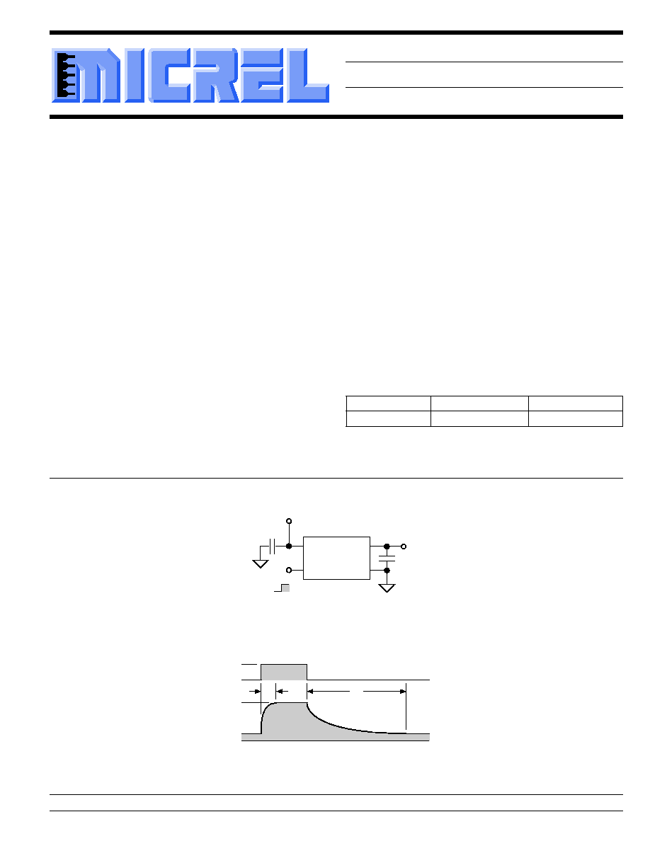
Typical Application
IN
OUT
MIC2660
1
3
GND
2
+3V Input
EN
5
0.01µF
+5V, 2.5mA*
Output
0.01µF
* The output is unregulated and
follows a load-line type function
Enable
Disable
Low-Current Unregulated Step-Up Supply
Timing Diagram
EN
0V
2V
OUT
5V
1V
0V
0.2
µs
1.3
µs
Output vs. Enable Input
Features
∑ 3V input produces approx. 5V unregulated output*
3.8mA with 1
µ
F external output capacitor
2.5mA without external capacitor
∑ 5V input produces approx. 9V unregulated output*
4.5mA output without external capacitor
∑ CMOS-logic compatible enable
∑ ESD protected
Applications
∑ Squib firing
∑ Refresh
∑ Burst/dump
∑ Low duty cycle load
∑ LCD bias generator
∑ Local 5V logic supply
∑ MOSFET driver
∑ Battery or solarcell boost
Ordering Information
Part Number
Temperature Range
Package
MIC2660BM5
≠40
∞
C to +85
∞
C
SOT-23-5
Micrel, Inc. ∑ 1849 Fortune Drive ∑ San Jose, CA 95131 ∑ USA ∑ tel + 1 (408) 944-0800 ∑ fax + 1 (408) 944-0970 ∑ http://www.micrel.com

MIC2660
Micrel
MIC2660
2
August 1999
Electrical Characteristics
Parameter
Condition (Note 1)
Min
Typ
Max
Units
Output Voltage, Enabled
V
IN
= 3V, V
EN
= V
IN
, C
OUT
= 1000pF, R
L
= 2k
4.5
5
V
V
IN
= 5V, V
EN
= V
IN
, C
OUT
= 1000pF, R
L
= 2k
8.1
9
V
Output Voltage, Disabled
V
IN
= 3V, V
EN
= GND, C
OUT
= 1000pF, R
L
= 2k
.9
1.0
1.3
V
V
IN
= 5V, V
EN
= GND, C
OUT
= 1000pF, R
L
= 2k
2.9
3.0
3.3
V
Input Current
V
IN
= 3V, V
EN
= V
IN
, R
L
= 2k
14.5
19.5
mA
V
IN
= 5V, V
EN
= V
IN
, R
L
= 2k
28.5
38.5
mA
Quiescent Current
V
IN
= 3V, V
EN
< 0.4V
1.5
3
µ
A
V
IN
= 5V, V
EN
< 0.4V
3.5
5
µ
A
Output Current
V
IN
= 3V, V
EN
= V
IN
, V
OUT
= V
OUT min
1.9
2.5
mA
V
IN
= 5V, V
EN
= V
IN
, V
OUT
= V
OUT min
3.4
4.5
mA
Enable Threshold
V
IN
= 3V
1.5
V
V
IN
= 5V
2.5
V
Enable Current
V
IN
= 5V, V
EN
= V
IN
10
µ
A
Turn-On Time
V
IN
= 3V
Load = 2k
, C
OUT
= 1000pF, Note 2
200
ns
Turn-Off Time
V
IN
= 3V
Load = 2k
, C
OUT
= 1000pF, Note 3
1.3
µ
s
General Note: Devices are ESD protected, however handling precautions are recommended.
Note 1:
Typicals values at T
A
= 25
∞
C. Minimum and maximum values at ≠40
∞
C
T
A
+85
∞
C.
Note 2:
Turn-on time is the time between V
EN
= 0.5
◊
V
IN
and V
OUT
= 0.9 (V
OUTmax
≠ V
OUTmin
) for a rising EN input.
Note 3:
Turn-off time is the time between V
EN
= 0.5
◊
V
IN
and V
OUT
= V
IN
≠ 1.9V for a falling EN input.
Pin Configuration
Part
Identification
IN
EN
NC
OUT
C10
1
3
4
5
2
GND
SOT-23-5 (M5)
Pin Description
Pin Number
Pin Name
Pin Function
1
IN
Supply (Input): +3V to +5V supply.
2
GND
Ground: Power return.
3
OUT
Output: Charge pump output. Connect to load.
4
NC
Not internally connected.
5
EN
Enable (Input): CMOS compatible input. EN high (V
EN
= V
IN
) enables the
charge pump . EN low (V
IN
= 0V) disables the charge pump.
Lead Temperature, Soldering 10sec. ........................ 300
∞
C
Package Thermal Resistance
SOT-23-5
JA
.................................................... 220
∞
C/W
SOT-23-5
JC
.................................................... 130
∞
C/W
Absolute Maximum Ratings
Input Voltage (V
IN
) ..................................................... +5.5V
Enable Voltage (V
EN
) ......................................... V
IN
+ 1.3V
Ambient Temperature Range (T
A
) ............. ≠40
∞
C to +85
∞
C
August 1999
3
MIC2660
MIC2660
Micrel
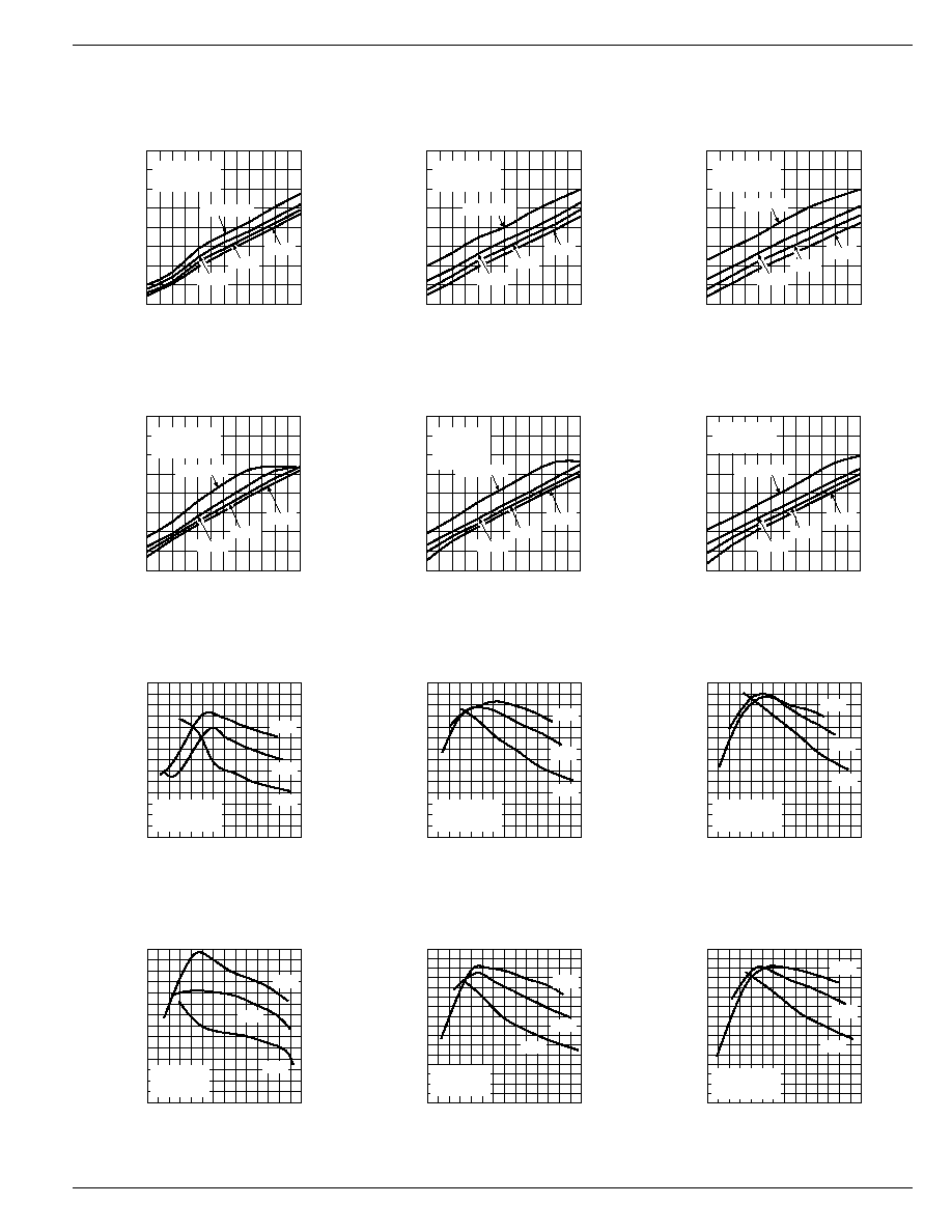
0
5
10
15
20
2.0
2.5
3.0
3.5
4.0
4.5
5.0
OUTPUT VOLTAGE (V)
SUPPLY VOLTAGE (V)
Output Voltage
vs. Supply Voltage
C
OUT
= NONE
T
A
= -55
∞
C
NO LOAD
1mA
2mA
3mA
0
5
10
15
20
2.0
2.5
3.0
3.5
4.0
4.5
5.0
OUTPUT VOLTAGE (V)
SUPPLY VOLTAGE (V)
Output Voltage
vs. Supply Voltage
C
OUT
= NONE
T
A
= 25
∞
C
NO LOAD
1mA
2mA
3mA
0
5
10
15
20
2.0
2.5
3.0
3.5
4.0
4.5
5.0
OUTPUT VOLTAGE (V)
SUPPLY VOLTAGE (V)
Output Voltage
vs. Supply Voltage
C
OUT
= NONE
T
A
= 125
∞
C
NO LOAD
1mA
2mA
3mA
0
5
10
15
20
2.0
2.5
3.0
3.5
4.0
4.5
5.0
OUTPUT VOLTAGE (V)
SUPPLY VOLTAGE (V)
Output Voltage
vs. Supply Voltage
C
OUT
= 1
µ
F
T
A
= -55
∞
C
NO LOAD
1mA
2mA
3mA
0
5
10
15
20
2.0
2.5
3.0
3.5
4.0
4.5
5.0
OUTPUT VOLTAGE (V)
SUPPLY VOLTAGE (V)
Output Voltage
vs. Supply Voltage
C
OUT
= 1
µ
F
T
A
= 25
∞
C
NO LOAD
1mA
2mA
3mA
0
5
10
15
20
2.0
2.5
3.0
3.5
4.0
4.5
5.0
OUTPUT VOLTAGE (V)
SUPPLY VOLTAGE (V)
Output Voltage
vs. Supply Voltage
C
OUT
= 1
µ
F
T
A
= 125
∞
C
NO LOAD
1mA
2mA
3mA
0
5
10
15
20
25
30
35
0
2
4
6
8
10
12
14
EFFICIENCY (%)
OUTPUT VOLTAGE (V)
Efficiency
vs. Output Voltage
C
OUT
= NONE
T
A
= -55
∞
C
1mA
2mA
3mA
0
5
10
15
20
25
30
35
0
2
4
6
8
10
12
14
EFFICIENCY (%)
OUTPUT VOLTAGE (V)
Efficiency
vs. Output Voltage
C
OUT
= NONE
T
A
= 25
∞
C
1mA
2mA
3mA
0
5
10
15
20
25
30
35
0
2
4
6
8
10
12
14
EFFICIENCY (%)
OUTPUT VOLTAGE (V)
Efficiency
vs. Output Voltage
C
OUT
= NONE
T
A
= 125
∞
C
1mA
2mA
3mA
0
5
10
15
20
25
30
35
0
2
4
6
8
10
12
14
EFFICIENCY (%)
OUTPUT VOLTAGE (V)
Efficiency
vs. Output Voltage
C
OUT
= 1
µ
F
T
A
= -55
∞
C
1mA
2mA
3mA
0
5
10
15
20
25
30
35
40
0
2
4
6
8
10
12
14
EFFICIENCY (%)
OUTPUT VOLTAGE (V)
Efficiency
vs. Output Voltage
C
OUT
= 1
µ
F
T
A
= 25
∞
C
1mA
2mA
3mA
0
5
10
15
20
25
30
35
40
0
2
4
6
8
10
12
14
EFFICIENCY (%)
OUTPUT VOLTAGE (V)
Efficiency
vs. Output Voltage
C
OUT
= NONE
T
A
= 125
∞
C
1mA
2mA
3mA
Typical Characteristics
MIC2660
Micrel
MIC2660
4
August 1999
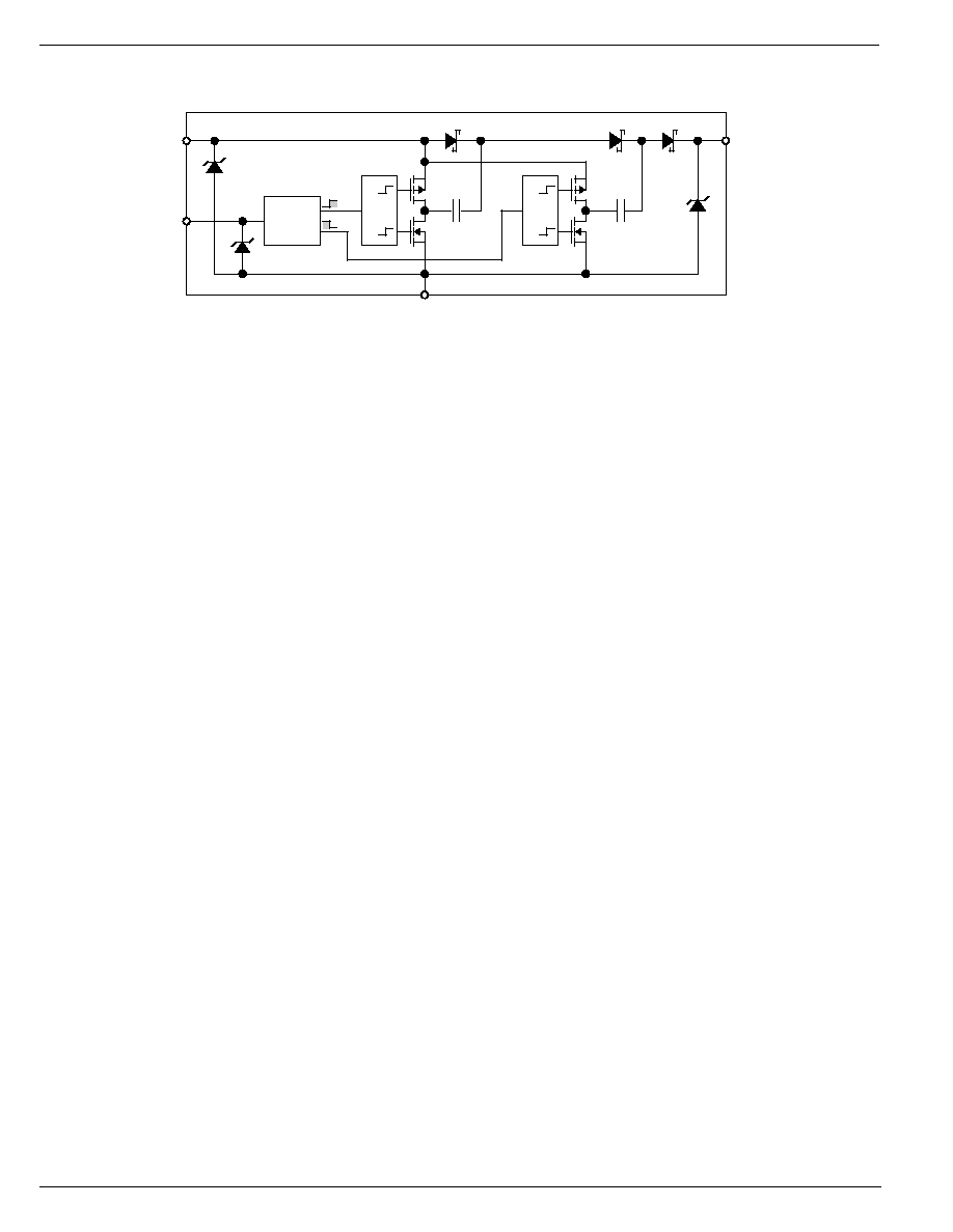
Block Diagram
OSC
EN
OUT
GND
IN
MIC2660
2
◊
3
◊
D1
D2
D3
C1
C2
XLO
XLO
Q1
Q2
Q4
Q3
Functional Description
Refer to the block diagram.
The MIC2660 charge pump consists of an oscillator and a
voltage tripler. A logic-high applied to EN activates the
charge pump. The charge pump produces an output voltage
that is higher than the input voltage.
Supply Input
IN (supply input) is rated for +2.7V to +5.5V.
Ouput
OUT is connected to IN, less 3 diode drops, at all times.
Enable
EN (enable) is a CMOS input. A logic low turns the oscillator
off. The threshold is approximately half the supply voltage. A
floating EN input may cause unpredictable operation.
Oscillator
The oscillator produces a square wave at approximately
18MHz. It has a noninverting and an inverting output.
Crossover Lockout
The charge pump contains two crossover lockout (XLO)
circuits. Each crossover lockout circuit drives a totem pole,
consisting of a P-channel MOSFET and an N-channel MOS-
FET. The crossover lockout alternately switches the MOS-
FETs with no significant transition current (shoot-through
current from supply to ground).
Tripler
Voltage stepup is performed by charging an internal capaci-
tor then switching the charged capacitor in series with the
supply voltage to produce a higher voltage. A description of
the nominal voltage tripler output is:
V
OUT
= 3V
IN
≠ 3V
D
.
where:
V
OUT
= output voltage
V
IN
= supply voltage
V
D
= voltage drop across forward biased diode
All formulas are simplified. Refer to the last paragraph of this
subsection about the actual output voltage.
The following sequence describes the basic operation of the
tripler by showing how the voltage at the "2
◊
" and "3
◊
" nodes,
V
2
◊
and V
3
◊
, increases.
Q2 turns on, completing the ground path to charge C1 (and
the 2
◊
node) to the supply voltage, less a diode voltage drop.
V
2
◊
(charging)
= V
IN
≠ V
D1
After Q2 turns off, Q1 turns on. The Q1-Q2 side of C1 is
switched (offset upward) from ground to V
IN
. The 2
◊
node,
that was nominally at the supply voltage, becomes nominally
twice the supply voltage.
V
2
◊
= V
IN
≠ V
D1
+ V
IN
While Q1 is on, Q4 is also on. When Q4 is on, the nominally
doubled voltage at the 2
◊
node is applied across C2, through
D2.
V
3
◊
(charging)
= V
IN
≠ V
D1
+ V
IN
≠ V
D2
After Q4 turns off, Q3 turns on. The Q3-Q4 side of C2 is
switched from ground to V
IN
. The 3
◊
node, that was nomi-
nally twice the supply voltage, becomes nominally three
times the supply voltage.
V
3
◊
= V
IN
≠ V
D1
+ V
IN
≠ V
D2
+ V
IN
The tripled voltage is available at the output through D3.
V
OUT
= V
IN
≠ V
D1
+ V
IN
≠ V
D2
+ V
IN
≠ V
D3
The output is nominally 3 times the supply voltage less the
voltage drop across three diodes.
The actual output is lower. These simplified formulas do not
show that the voltage across the capacitors decreases when
charge flows to the following stage or output. An actual
device also has some internal loss.
ESD Protection
Zener diodes are provided at IN, EN, and OUT to limit ESD
voltage.

August 1999
5
MIC2660
MIC2660
Micrel
Applications Information
Electromagnetic Interference
The 18MHz oscillator may cause interference to radio cir-
cuits. 0.01
µ
F bypass capacitors should be mounted close to
the IN and OUT terminals.
Low-Side MOSFET Charge-Pump Driver
A standard MOSFET requires approximately 15V to fully
enhance the gate for minimum R
DS
(on)
. Substituting a logic-
level MOSFET reduces the required gate voltage, allowing
an MIC2660 to be used as an low-side FET driver.
A 3V powered MIC2660 will fully enhance a logic-level
N-channel MOSFET low-side switch, with a 5k gate pull-
down resistor, in less than 1ms after the enable pin rises
above 1.5V. The 1nF MOSFET gate capacitance will be
discharged to turn-off in less than 10ms after the enable pin
goes below 1.5V.
Enable
Disable
IN
OUT
MIC2660
1
3
GND
2
+3V to +5V
EN
5
Load
Supply
R
LOAD
1µF
0.1µF
100k
Figure 1. Charge-Pump Driver
An MIC2660 boosts a 5V input to 9V≠12V to fully enhance an
N-channel MOSFET, which may have its drain connected to
a higher voltage, through a high-side load. A TTL high signal
applied to CS enables the internal oscillator, which quickly
develops 9V≠12V at the gate of the MOSFET, clamped by a
zener diode. A resistor from the gate to ground ensures that
the FET will turn off quickly when the MIC2660 is turned off.
Charge-Pump/Dump
A large capacitor can be charged to the unloaded tripled
voltage output after a time based on the maximum current
provided by the MIC2660. A 1000
µ
F Capacitor can be
charged from 2V to approximately 12V in less than 3 seconds
by a 5V powered MIC2660. (i = C
dv/dt).
Once charged, a maximum current of 3mA may be drawn
continuously at the 12V level. A high value bleeder resistor
(100k) is not needed to prevent spikes from exceeding the
capacitor voltage rating, since the MIC2660's internal 15V
ESD zener limits maximum output. A 68
resistor in series
with the output limits short-circuit current to 30mA.
IN
OUT
MIC2660
1
3
GND
2
+5V
EN
5
+12V
1000µF
0.1µF
100k
68
Figure 2. Charge-Pump/Dump
5-Volt Lamp Flasher
An IttyBitty MIC1557 oscillator provides a short pulse once
per second, enabling the CS pin of an MIC2660, which
charges the gate-to-drain capacitance of a logic-level
N-channel MOSFET to approximately 9V, which turns on a
lamp. When the CS pin is low, a 2k resistor discharges the
gate capacitance, turning off the lamp. A resistor (R
S
) in
series with a diode determines the "on" time to approximately
R
S
||R
T
◊
C
T
,while R
T
and C
T
set the "off" time to 1.1R
T
◊
C
T
.
IN
OUT
MIC2660
1
3
GND
2
EN
5
VS
CS
MIC1557
4
3
GND
2
+5V
OUT
5
T/T
1
5V lamp
C
T
0.68µF
IRL3103
N-channel
FET
0.1µF
2k
R
S
470k
R
T
1M
Figure 3. 5-Volt Lamp Flasher