September 2000
1
MIC2777
MIC2777
Micrel
MIC2777
Dual Micro-Power Low Voltage Supervisor
Final Information
General Description
The MIC2777 is a dual power supply supervisor that provides
under-voltage monitoring, manual reset capability, and power-
on reset generation in a compact 5-pin SOT package. Fea-
tures include two under-voltage detectors, one fixed and one
adjustable, and both active-high and active-low reset out-
puts. One under-voltage detector compares V
DD
against a
fixed threshold. Ten factory-programmed thresholds are avail-
able. The other under-voltage detector is user-adjustable.
The reset outputs are asserted for no less than 140ms at
power-on and any time V
DD
or the input voltage drops below
the corresponding reference voltage. They remain asserted
for the timeout period after the input voltage and V
DD
subse-
quently rise back above the threshold boundaries. A reset
can be generated at any time by pulling down on the adjust-
able input. Hysteresis is included to prevent chattering due to
noise. Typical supply current is a low 3.5
µ
A.
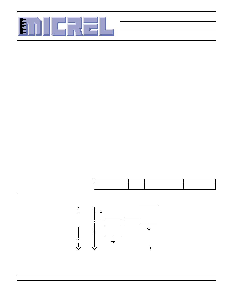
Typical Application
IN
R1
R2
/RST
VDD
RST
OTHER
LOGIC
MIC2777
MICROPROCESSOR
Manual
Reset
/RESET
V
CORE
V
CORE
1.0V
V
I/O
1.8V
V
I/O
GND
GND
Typical Application
Features
∑ Monitors two independent power supplies for under-
voltage conditions
∑ One fixed and one user adjustable input
∑ 1.5% theshold accuracy
∑ Choice of factory-programmed thresholds
∑ User-adjustable input can monitor supplies as low as
0.3V
∑ Generates 140ms (minimum) power-on RESET pulse
∑ Manual reset capability
∑ Both active-high and active-low RESET outputs
∑ Input may be pulled above V
DD
(abs. max.)
∑ /RST output valid down to 1.2V
∑ Ultra-low supply current, 3.5
µ
A typical
∑ Rejects brief input transients
∑ IttyBittyTM 5-lead SOT-23 package
Applications
∑ Monitoring processor, ASIC, or FPGA core and I/O
voltages
∑ Computer systems
∑ PDAs, hand-held PCs
∑ Embedded controllers
∑ Telecommunications systems
∑ Power supplies
∑ Wireless / Cellular systems
∑ Networking hardware
Micrel, Inc. ∑ 1849 Fortune Drive ∑ San Jose, CA 95131 ∑ USA ∑ tel + 1 (408) 944-0800 ∑ fax + 1 (408) 944-0970 ∑ http://www.micrel.com
IttyBittyTM is a trademark of Micrel, Inc.
Ordering Information
Part Number
Marking
Junction Temp. Range
Package
MIC2777-XXBM5
UNXX
≠40
∞
C to +85
∞
C
SOT-23-5
MIC2777
Micrel
MIC2777
2
September 2000
Pin Configuration
/RST
VDD
IN
RST
1
3
4
5
2
GND
SOT-23-5 (M5)
Standard Voltage Options*
Voltage
Typical
Nominal Threshold
Code
Application (V
DD
)
Voltage (V
TH
)
46
5.0V
±
5%
4.68
44
5.0V
±
10%
4.43
31
3.3V
±
5%
3.09
29
3.3V
±
10%
2.93
28
3.0V
±
5%
2.81
26
2.85V
±
5%
2.67
25
2.70V
±
5%
2.53
23
2.5V
±
5%
2.34
22
2.4V
±
5%
2.25
17
1.8V
±
5%
1.69
*There are ten standard versions available with an order increment of 3000 pieces. Samples of standard versions are
normally available from stock. Contact factory for information on non-standard versions. Available in tape-and-reel only.
Pin Description
Pin Number
Pin Name
Pin Function
1
/RST
Digital (Output): Asserted low whenever V
IN
or V
DD
falls below the reference
voltage. It will remain asserted for no less than 140ms after V
IN
and V
DD
return above the threshold limits.
2
GND
Ground
3
RST
Digital (Output): Asserted high whenever V
IN
or V
DD
falls below the refer-
ence voltage. It will remain asserted for no less than 140ms after V
IN
and
V
DD
return within above the threshold limit.
4
IN
Analog (Input): The voltage on this pin is compared to the internal 300mV
reference. An undervoltage condition will trigger a reset sequence. Manual
reset capability can be achieved by adding a switch between this pin and
ground.
5
VDD
Analog (Input): Power supply input for internal circuitry and input to the fixed
voltage monitor: The votage on this pin is compared against the internal
voltage reference. An undervoltage condition will trigger a reset sequence.
September 2000
3
MIC2777
MIC2777
Micrel
Absolute Maximum Ratings
(Note 1)
Supply Voltage (V
DD
) ..................................... ≠0.3V to +7V
Input Voltage (V
IN
) ......................................... ≠0.3V to +7V
RST, (/RST) Current .................................................. 20mA
Storage Temperature (T
S
) ....................... ≠65
∞
C to +150
∞
C
ESD Rating, Note 3 ................................................... 1.5kV
Operating Ratings
(Note 2)
Supply Voltage (V
DD
) .................................. +1.5V to +5.5V
Input Voltage
(V
IN
) ........................................................... ≠0.3V to +6.0V
Ambient Temperature Range (T
A
) ............. ≠40
∞
C to +85
∞
C
Package Thermal Resistance (
JA
) ...................... 256
∞
C/W
Electrical Characteristics
Note 5; T
A
= +25
∞
C, bold values indicate ≠40
∞
C
T
A
+85
∞
C; unless noted
Symbol
Parameter
Condition
Min
Typ
Max
Units
I
DD
Supply Current
V
DD
= V
IN
3.5
µ
A
Note 5; /MR, RST, /RST open
VDD VOLTAGE THRESHOLD
Under-Voltage Threshold On V
DD
V
TH
-1.5%
V
TH
V
TH
+1.5%
V
V
HYST
Hysteresis Voltage
1
%
IN, UNDER-VOLTAGE DECTECTOR INPUT
V
REF
Under-Voltage Threshold
295
300
305
mV
V
HYST
Hysteresis Voltage
3
mV
I
IN
Input Current
5
pA
T
MIN
T
A
T
MAX
10
nA
RST, /RST OUTPUTS
t
PROP
Propagation Delay
V
IN
= (V
REF(MAX)
+ 100mV) to
20
µ
s
V
IN
= (V
REF(MIN)
≠ 100mV) or
V
DD
= (V
TH
+ 2.5%) to (V
TH
≠ 2.5%), V
IN
=V
DD
t
RST
Reset Pulse Width
140
280
ms
V
OL
RST or /RST Output Voltage Low
I
SINK
= 1.6mA;
0.3
V
V
DD
1.6V
I
SINK
= 100
µ
A;
0.3
V
V
DD
1.2V,
Note 4
V
OH
RST or /RST Output Voltage High
I
SOURCE
= 500
µ
A;
0.8V
DD
V
V
DD
1.5V
RST asserted, I
SOURCE
= 10
µ
A;
0.8V
DD
V
V
DD
1.2V,
Note 4
Note 1.
Exceeding the absolute maximum rating may damage the device.
Note 2.
The device is not guaranteed to function outside its operating rating.
Note 3.
Devices are ESD sensitive. Handling precautions recommended. Human body model, 1.5k in series with 100pF.
Note 4.
V
DD
operating range is 1.5V to 5.5V. Output is guaranteed to be asserted down to V
DD
= 1.2V.
Note 5.
V
DD
equals the nominal "Typical Application (V
DD
)" as shown in "Standard Voltage Options Table."

MIC2777
Micrel
MIC2777
4
September 2000
Timing Diagram
V
TH
V
IN
0V
V
HYST
V
DD
0V
V
/RST
(ACTIVE LOW)
V
OH
V
OL
V
RST
(ACTIVE HIGH)
V
OH
V
OL
t
RST
t
RST
A
A
A
V
REF
V
HYST
Propagation delays not shown for clarity.
Note A.
The MIC2777 ignores very brief transients.
See "Applications Information" for details.
September 2000
5
MIC2777
MIC2777
Micrel
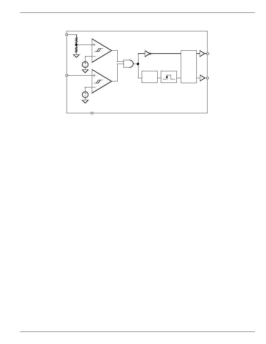
Functional Diagram
GND
V
DD
IN
MIC2777
V
REF
V
REF
RST
R
S
Q
/Q
/RST
Delay
Line
One Shot
Functional Description
IN, Under-Voltage Detector Input
The voltage present at the IN pin is compared to the internal
300mV reference voltage. A reset is triggered if and when V
IN
falls below V
REF
. Typically, a resistor divider is used to scale
the input voltage to be monitored such that V
IN
will fall below
V
REF
as the voltage being monitored falls below the desired
trip-point. Hysteresis is employed to prevent chattering due to
noise. The comparator on the IN input is relatively immune to
very brief negative-going transients.
V
DD
Input
The V
DD
pin is both the power supply terminal and a moni-
tored input voltage. The voltage at this pin is continually
compared against the internal reference. The trip-point at
which a reset occurs is factory programmed. A reset is
triggered if and when V
DD
falls below the trip-point. Hyster-
esis is employed to prevent chattering due to noise. The
comparator on the V
DD
input is relatively immune to very brief
negative-going transients.
RST, /RST Reset Output
Typically, the MIC2777 is used to monitor the power supplies
of intelligent circuits such as microcontrollers and micropro-
cessors. By connecting the appropriate reset output of a
MIC2777 to the reset input of a
µ
C or
µ
P, the processor will
be properly reset at power-on and during power-down and
brown-out conditions.
The reset outputs are asserted any time V
DD
or V
IN
drops
below the corresponding threshold voltage. The reset out-
puts remain asserted for t
RST
(min) after V
IN
and/or V
DD
subsequent return above the threshold boundaries and/or
/MR is released. A reset pulse is also generated at power-on.
Manual Reset
The ability to initiate a reset via external logic or a manual
switch is provided in addition to the MIC2777's automatic
supervisory functions. Typically, a momentary push-button
switch is connected such that IN is shorted to ground when
the switch contacts close. Assuming V
DD
and V
IN
are within
tolerance when the switch is released, the reset outputs will
be de-asserted no less than 140ms later. IN can also be
driven by an open-drain or open-collector logic signal.

MIC2777
Micrel
MIC2777
6
September 2000
Application Information
Programming the Voltage Threshold
Referring to the "Typical Application Circuit", the voltage
threshold on the IN pin is calculated as follows:
V
V
R1 R2
R2
TH
REF
=
◊
+
(
)
where V
REF
= 0.300V
In order to provide the additional criteria needed to solve for
the resistor values, the resistors can be selected such that the
two resistors have a given total value, that is, R1 + R2 =
R
TOTAL
. Imposing this condition on the resistor values pro-
vides two equations that can be solved for the two unknown
resistor values. A value such as 1M
for R
TOTAL
is a
reasonable choice since it keeps quiescent current to a
generally acceptable level while not causing any measurable
errors due to input bias currents. The larger the resistors, the
larger the potential errors due to input bias current (I
IN
). The
maximum recommended value of R
TOTAL
is 3M
.
Applying this criteria and rearranging the V
TH
expression to
solve for the resistor values gives:
R2
R
V
V
TOTAL
REF
TH
=
(
)
(
)
R1
R
R2
TOTAL
=
-
Application Example
Figure 1 below illustrates a hypothetical MIC2777-23 applica-
tion in which the MIC2777-23 is used to monitor the core and
I/O supplies of a high-performance CPU or DSP. The core
supply, V
CORE
, in this example is 1.0V
±
5%. The main power
rail and I/O voltage, V
I/O
, is 2.5V
±
5%. As shown in Figure 1,
the MIC2777 is powered by V
I/O
. The minimum value of V
I/O
is 2.5V ≠5% = 2.375V; the maximum is 2.5V +5% = 2.625V.
This is well within the MIC2777's power supply range of 1.5V
to 5.5V.
Resistors R1 and R2 must be selected to correspond to the
V
CORE
supply of 1.0V. The goal is to insure that the core
supply voltage is adequate to insure proper operation, i.e.,
V
CORE
(1.0V ≠5%) = 0.950V. Because there is always a
small degree of uncertainty due to the accuracy of the
resistors, variations in the devices' voltage reference, etc.,
the threshold will be set slightly below this value. The poten-
tial variation in the MIC2777's input voltage reference (V
REF
)
is specified as
±
1.5%. The resistors chosen will have their
own tolerance specification. This example will assume the
use of 1% accurate resistors. The potential worst-case error
contribution due to input bias current can be calculated once
the resistor values are chosen. If the guidelines above
regarding the maximum total value of R1+R2 are followed,
this error contribution will be very small thanks to the MIC2777's
very low input bias current.
To summarize, the various potential error sources are:
∑ Variation in V
REF
:
specified at
±
1.5%
∑ Resistor tolerance:
chosen by designer (typically
±
1%)
∑ Input bias current, I
IN
:
calculated once resistor values are known, typically
very small
Taking the various potential error sources into account, the
threshold voltage will be set slightly below the minimum
V
CORE
specification of 0.950V so that when the actual thresh-
old voltage is at its maximum, it will not intrude into the normal
operating range of V
CORE
. The target threshold voltage will
be set as follows:
Given that the total tolerance on V
TH
for the IN pin is [V
REF
tolerance] + [resistor tolerance]
=
±
1.5% +
±
1% =
±
2.5%,
and V
TH(max)
= V
CORE(min)
,
then V
CORE(min)
= V
TH
+ 2.5% V
TH
= 1.025 V
TH
,
therefore, solving for V
TH
results in
V
=
V
1.025
=
0.950
1.025
= 0.9268V
TH
CORE(min)
Solving for R1 and R2 using this value for V
TH
and the
equations above yields:
R1 = 676.3k
673k
R2 = 323.7k
324k
The resulting circuit is shown in Figure 1.
Input Bias Current Effects
Now that the resistor values are known, it is possible to
calculate the maximum potential error due to input bias
current, I
IN
. As shown in the "Electrical Characteristics" table,
the maximum value of I
IN
is 10nA. (Note that the typical value
is a much smaller 5pA!) The magnitude of the offset caused
by I
IN
is given by:
V
I
R1|| R2
ERROR
IN(max)
=
◊
(
)
=
V
1 10
A
2.189 10
=
ERROR
5
= ± ◊
◊
◊
-
8
V
2.189 10
V =
ERROR
3
= ±
◊
-
V
2.189mV
ERROR
= ±
The typical error is about three orders of magnitude lower
than this - close to one
microvolt! Generally, the error due
to input bias can be discounted. If it is to be taken into
account, simply adjust the target threshold voltage
downward by this amount and recalculate R1 and R2. The
resulting value will be very close to optimum. If accuracy
is more important than the quiescent current in the
resistors, simply reduce the value of R
TOTAL
to minimize
offset errors.
September 2000
7
MIC2777
MIC2777
Micrel
IN
/RST
RST
VDD
GND
MIC2777-23
R1
676k
1%
R2
324k
1%
/RESET
VCORE
GND
V
CORE
1.0V
±
5%
MICROPROCESSOR
VI/O
V
I/O
2.5V
±
5%
Figure 1. MIC2777 Example Design
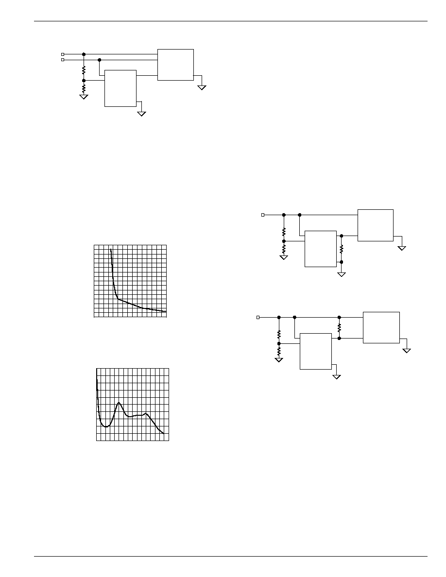
Transient response
The MIC2777 is inherently immune to very short negative-
going "glitches." Very brief transients may exceed the voltage
thresholds without tripping the output.
As shown in Figure 3a and 3b, in general the narrower the
transient, the deeper the threshold overdrive that will be
ignored by the MIC2777. The graph represents the typical
allowable transient duration for a given amount of threshold
overdrive that will not generate a reset.
0
5
10
15
20
25
30
35
40
0
100
200
300
MAX. TRANSIENT DURATION (
µ
s)
RESET COMP. OVERDRIVE, V
REF
≠V
IN
(mV)
Typical INPUT
Transient Response
Figure 3a. Typical INPUT Transient Response
0
20
40
60
80
100
0
500
1000
1500
2000
MAX. TRANSIENT DURATION (
µ
s)
RESET COMP. OVERDRIVE, V
REF
≠V
DD
(mV)
Typical V
DD
Transient Response
Figure 3b. Typical V
DD
Transient Response
Ensuring Proper Operation at Low Supply
At levels of V
DD
below 1.2V, the MIC2777's /RST output
cannot turn on sufficiently to produce a valid logic-low on
/RST. In this situation, other circuits driven by /RST could be
allowed to float, causing undesired operation. (In most cases,
however, it is expected that the circuits driven by the MIC2777
will be similarly inoperative at V
DD
1.2V.)
If a given application requires that /RST be valid below V
DD
= 1.2V, this can be accomplished by adding a pull-down
resistor to the /RST output. A value of 100k
is recom-
mended as this is usually an acceptable compromise of
quiescent current and pull-down current. The resistor's value
is not critical, however. See Figure 4.
The statements above also apply to the MIC2777's RST
output. That is, to ensure valid RST signal levels at V
DD
<
1.2V, a pull-up resistor (as opposed to a pull-down) should be
added to the RST output. A value of 100k
is typical for this
application as well. See Figure 5.
IN
/RST
RST
VDD
GND
MIC2777-XX
R1
R2
/RESET
VCC
GND
V
CC
MICROPROCESSOR
100k
Rpull-down
Figure 4. MIC2777 Valid /RST Below 1.2V
IN
RST
/RST
VDD
GND
MIC2777-XX
R1
R2
RESET
VCC
GND
V
CC
MICROPROCESSOR
100k
Rpull-up
Figure 5. MIC2777 Valid RST Below 1.2V
MIC2777
Micrel
MIC2777
8
September 2000
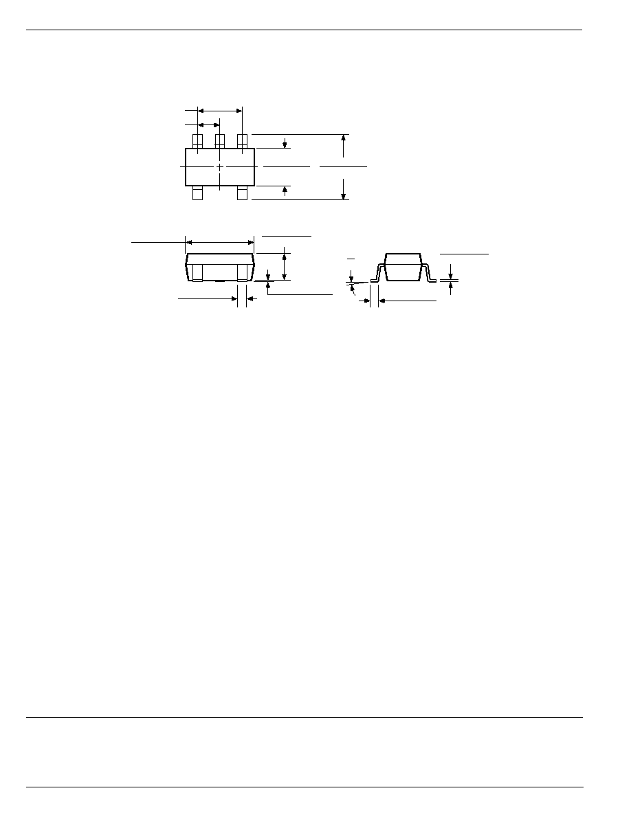
Package Information
0.20 (0.008)
0.09 (0.004)
0.60 (0.024)
0.10 (0.004)
3.02 (0.119)
2.80 (0.110)
10
∞
0
∞
3.00 (0.118)
2.60 (0.102)
1.75 (0.069)
1.50 (0.059)
0.95 (0.037) REF
1.30 (0.051)
0.90 (0.035)
0.15 (0.006)
0.00 (0.000)
DIMENSIONS:
MM (INCH)
0.50 (0.020)
0.35 (0.014)
1.90 (0.075) REF
SOT-23-5 (M5)
MICREL INC.
1849 FORTUNE DRIVE
SAN JOSE, CA 95131
USA
TEL
+ 1 (408) 944-0800
FAX
+ 1 (408) 944-0970
WEB
http://www.micrel.com
This information is believed to be accurate and reliable, however no responsibility is assumed by Micrel for its use nor for any infringement of patents or
other rights of third parties resulting from its use. No license is granted by implication or otherwise under any patent or patent right of Micrel Inc.
© 2000 Micrel Incorporated