
September 29, 2000
1
MIC284
MIC284
Micrel
MIC284
Two-Zone Thermal Supervisor
Advance Information
Typical Application
CLK
FROM
SERIAL BUS
HOST
OVER-TEMP
SHUTDOWN
REMOTE
DIODE
2200pF
0.1
µF
MIC284
/INT
/CRIT
3.3V
DATA
4
◊ 10k
pull-ups
VDD
T1
A0
GND
2-Channel SMBus Temperature Measurement System
Features
∑ Optimized for CPU Thermal Supervision in Computing
Applications
∑ Measures Local and Remote Temperature
∑ Sigma-Delta ADC for 8-Bit Temperature Results
∑ 2-Wire SMBus-compatible Interface
∑ Programmable Thermostat Settings for both Internal and
External Zones
∑ Open-Drain Interrupt Output Pin
∑ Open-Drain Over Temperature Output Pin for Fan
Control or Hardware Shutdown
∑ Interrupt Mask and Status Bits
∑ Low Power Shutdown Mode
∑ Failsafe response to diode faults
∑ 2.7V to 5.5V Power Supply Range
∑ 8-Lead SOIC and MSOP Packages
Applications
∑ Desktop, Server and Notebook Computers
∑ Power Supplies
∑ Test and Measurement Equipment
∑ Wireless Systems
∑ Networking/Datacom Hardware
Micrel, Inc. ∑ 1849 Fortune Drive ∑ San Jose, CA 95131 ∑ USA ∑ tel + 1 (408) 944-0800 ∑ fax + 1 (408) 944-0970 ∑ http://www.micrel.com
General Description
The MIC284 is a versatile digital thermal supervisor capable
of measuring temperature using its own internal sensor and
an inexpensive external sensor or embedded silicon diode
such as those found in the Intel Pentium III* CPU. A 2-wire
serial interface is provided to allow communication with either
I
2
C** or SMBus* masters. Features include an open-drain
over-temperature output with dedicated registers for imple-
menting fan control or over-temperature shutdown circuits.
Interrupt status and mask bits are provided for reduced
software overhead. The open-drain interrupt output pin can
be used as either an overtemperature alarm or a thermostatic
control signal. A programmable address pin permits two
devices to share the bus. (Alternate base addresses avail-
able-contact Micrel.) Superior performance, low power and
small size makes the MIC284 an excellent choice for the most
demanding thermal management applications.
*SMBus and Pentium III are trademarks of Intel Corporation.
**I
2
C is a trademark of Philips Electronics, N.V.
Ordering Information
Part Number
Base Address
(
*
)
Junction Temp. Range
Package
Notes
MIC284-0BM
100 100x
≠55
∞C to +125∞C
8-Lead SOP
MIC284-1BM
100 101x
≠55
∞C to +125∞C
8-Lead SOP
Contact Factory
MIC284-2BM
100 110x
≠55
∞C to +125∞C
8-Lead SOP
Contact Factory
MIC284-3BM
100 111x
≠55
∞C to +125∞C
8-Lead SOP
Contact Factory
MIC284-0BMM
100 100x
≠55
∞C to +125∞C
8-Lead MSOP
MIC284-1BMM
100 101x
≠55
∞C to +125∞C
8-Lead MSOP
Contact Factory
MIC284-2BMM
100 110x
≠55
∞C to +125∞C
8-Lead MSOP
Contact Factory
MIC284-3BMM
100 111x
≠55
∞C to +125∞C
8-Lead MSOP
Contact Factory
* The least-significant bit of the slave address is determined by the state of the A0 pin.

MIC284
Micrel
MIC284
2
September 29, 2000
Pin Description
Pin Number
Pin Name
Pin Function
1
DATA
Digital I/O: Open-drain. Serial data input/output.
2
CLK
Digital Input: The host provides the serial bit clock on this input.
3
/INT
Digital Output: Open-drain. Interrupt or thermostat output.
4
GND
Ground: Power and signal return for all IC functions.
5
/CRIT
Digital Output: Open-Drain. Over-temperature indication
6
T1
Analog Input: Connection to remote temperature sensor (diode junction)
7
A0
Digital Input: Slave address selection input. See Table 1. MIC284 Slave
Address Settings.
8
VDD
Analog Input: Power supply input to the IC.
Pin Configuration
1
DATA
CLK
/INT
GND
8
VDD
A0
T1
/CRIT
7
6
5
2
3
4

September 29, 2000
3
MIC284
MIC284
Micrel
Absolute Maximum Ratings
(Note 1)
Power Supply Voltage, V
DD ...................................................
6.0V
Voltage on Any Pin ................................ ≠0.3V to V
DD
+0.3V
Current Into Any Pin ................................................
±10 mA
Power Dissipation, T
A
= +125
∞C ............................... 30mW
Junction Temperature ............................................. +150
∞C
Storage Temperature ............................... ≠65
∞C to +150∞C
ESD Ratings (Note 3)
Human Body Model .................................................. TBD V
Machine Model ......................................................... TBD V
Soldering
Vapor Phase (60 sec.) ............................. +220
∞C
+5
/
≠0
∞C
Infrared (15 sec.) ...................................... +235
∞C
+5
/
≠0
∞C
Operating Ratings
(Note 2)
Power Supply Voltage, V
DD ..............................
+2.7V to +5.5V
Ambient Temperature Range (T
A
) ............ -55
∞C to +125∞C
Package Thermal Resistance (
JA
)
SOP ................................................................. +152
∞C/W
MSOP .............................................................. +206
∞C/W
Electrical Characteristics
2.7V
V
DD
5.5; T
A
= +25
∞C, bold values indicate ≠55∞C T
A
+125∞C, Note 4; unless noted.
Symbol
Parameter
Condition
Min
Typ
Max
Units
Power Supply
I
DD
Supply Current
/INT, open, A0 = V
DD
or GND,
350
750
µA
CLK = DATA = high, normal mode
/INT, /CRIT open, A0 = V
DD
or GND
shutdown mode, CLK = 100kHz
3
µA
/INT, /CRIT open, A0 = V
DD
or GND
shutdown mode, CLK = DATA = high
1
10
µA
t
POR
Power-On Reset Time, Note 7
V
DD
> V
POR
200
µs
V
POR
Power-On Reset Voltage
all registers reset to default values,
2.0
2.7
V
A/D conversions initiated
V
HYST
Power-On Reset Hysteresis Voltage
250
mV
Temperature-to-Digital Converter Characteristics
Accuracy--Local Temperature
0
∞C T
A
+100∞C, /INT and /CRIT open,
±1
±
2
∞C
Note 4, 9
3V
V
DD
3.6V
≠55
∞C T
A
+125∞C, /INT and /CRIT open,
±2
±
3
∞C
3V
V
DD
3.6V
Accuracy--Remote Temperature
0
∞C T
D
+100∞C, /INT and /CRIT open,
±1
±
3
∞C
Note 4, 5, 9
3V
V
DD
3.6V, 0∞C T
A
+85∞C
≠55
∞C T
D
+125∞C, /INT and /CRIT open,
±2
±
5
∞C
3V
V
DD
3.6V, 0∞C T
A
+85∞C
t
CONV0
Conversion Time, local zone
50
80
ms
Note 7
t
CONV1
Conversion Time, remote zone
Note 7
100
160
ms
Remote Temperature Input (T1)
I
F
Current to External Diode
high level, T1 forced to 1.5V
224
400
µA
Note 7
low level
7.5
14
µA
Address Input (A0)
V
IL
Low Input Voltage
2.7V
V
DD
5.5V
0.6
V
V
IH
High Input Voltage
2.7V
V
DD
5.5V
2.0
V
C
IN
Input Capacitance
10
pF
I
LEAK
Input Current
±0.01
±
1
µA

MIC284
Micrel
MIC284
4
September 29, 2000
Symbol
Parameter
Condition
Min
Typ
Max
Units
Serial Data I/O Pin (DATA)
V
OL
Low Output Voltage
I
OL
= 3mA
0.4
V
Note 6
I
OL
= 6mA
0.8
V
V
IL
Low Input Voltage
2.7V
V
DD
5.5V
0.3V
DD
V
V
IH
High Input Voltage
2.7V
V
DD
5.5V
0.7V
DD
V
C
IN
Input Capacitance
10
pF
I
LEAK
Input current
±0.01
±
1
µA
Serial Clock Input (CLK)
V
IL
Low Input Voltage
2.7V
V
DD
5.5V
0.3V
DD
V
V
IH
High Input Voltage
2.7V
V
DD
5.5V
0.7V
DD
V
C
IN
Input Capacitance
10
pF
I
LEAK
Input current
±0.01
±
1
µA
Status Output (/INT)
V
OL
Low Output Voltage,
I
OL
= 3mA
0.4
V
Note 6
I
OL
= 6mA
0.8
V
t
INT
Interrupt Propagation Delay,
from TEMP > T_SET or TEMPx < T_HYSTx
t
CONV
+1
µs
Note 7, 8
to INT < V
OL
, FQ = 00, R
PULLUP
= 10k
t
nINT
Interrupt Reset Propagation Delay,
from any register read to /INT > V
OH
1
µs
Note 7
FQ = 00, R
PULLUP
= 10k
T_SET0
Default T_SET0 Value
t
POR
after V
DD
> V
POR
81
81
81
∞C
T_HYST0
Default T_HYST0 Value
t
POR
after V
DD
> V
POR
76
76
76
∞C
T_SET1
Default T_SET1 Value
t
POR
after V
DD
> V
POR
97
97
97
∞C
T_HYST1
Default T_HYST1 Value
t
POR
after V
DD
> V
POR
92
92
92
∞C
Over-Temperature Output (/CRIT)
V
OL
Low Output Voltage,
I
OL
= 3mA
0.4
V
Note 6
I
OL
= 6mA
0.8
V
t
CRIT
/CRIT Propagation Delay,
from TEMPx > T_SETx or TEMPx < T_HYSTx
t
CONV
+1
µs
Note 7, 8
to INT < V
OL
, FQ = 00, R
PULLUP
= 10k
t
nCRIT
/CRIT Reset Propagation Delay,
from TEMPx < nCRITx to /CRIT > V
OH
1
µs
Note 7
FQ = 00, R
PULLUP
= 10k
CRIT1
Default CRIT1 Value
t
POR
after V
DD
> V
POR
97
97
97
∞C
nCRIT1
Default nCRIT1 Value
t
POR
after V
DD
> V
POR
92
92
92
∞C
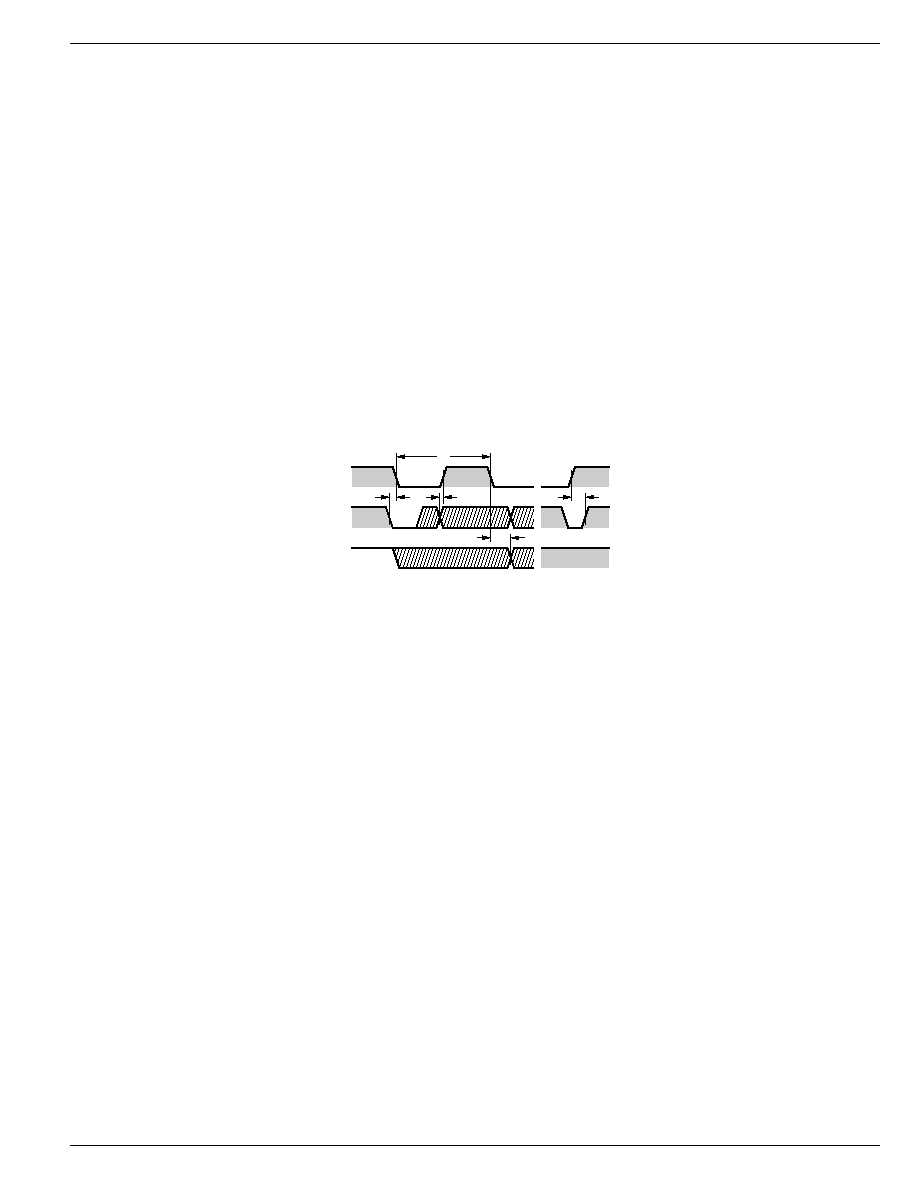
Serial Interface Timing (Note 7)
t
1
CLK (Clock) Period
2.5
µs
t
2
Data In Setup Time to CLK High
100
ns
t
3
Data Out Stable After CLK Low
0
ns
t
4
DATA Low Setup Time to CLK Low
start condition
100
ns
t
5
DATA High Hold Time
stop condition
100
ns
After CLK High
September 29, 2000
5
MIC284
MIC284
Micrel
Note 1.
Exceeding the absolute maximum rating may damage the device.
Note 2.
The device is not guaranteed to function outside its operating rating.
Note 3.
Devices are ESD sensitive. Handling precautions recommended.
Human body model: 1.5k in series with 100pF. Machine model: 200pF, no series resistance.
Note 4.
Final test on outgoing product is performed at T
A
= TBD
∞C.
Note 5.
T
D
is the temperature of the remote diode junction. Testing is performed using a single unit of one of the transistors listed in Table 6.
Note 6.
Current into this pin will result in self-heating of the MIC284. Sink current should be minimized for best accuracy.
Note 7.
Guaranteed by design over the operating temperature range. Not 100% production tested.
Note 8.
t
CONV
= t
CONV0
+ t
CONV1
. t
CONV0
is the conversion time for the local zone; t
CONV1
is the conversion time for the remote zone.`
Note 9.
Accuracy specification does not include quantization noise, which may be as great as
±
1
/
2
LSB (
±0.5∞C).
Timing Diagram
t
1
t
2
t
5
t
4
t
3
SCL
SDA Data In
SDA Data Out
Serial Interface Timing
MIC284
Micrel
MIC284
6
September 29, 2000
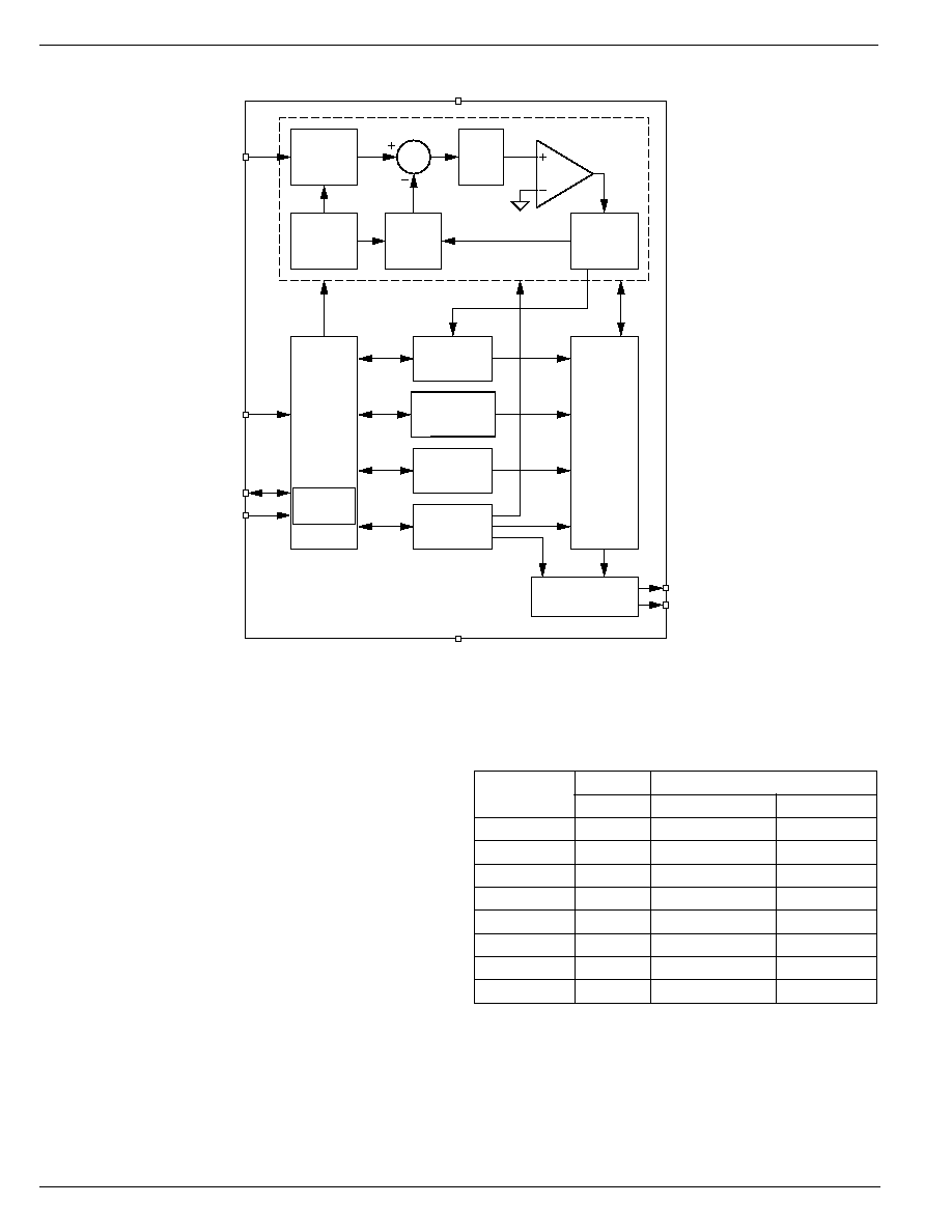
FUNCTIONAL DESCRIPTION
Pin Descriptions
VDD: Power supply input. See electrical specifications.
GND: Ground return for all MIC284 functions.
CLK: Clock input to the MIC284 from the two-wire serial bus.
The clock signal is provided by the host, and is shared by all
devices on the bus.
DATA: Serial data I/O pin that connects to the two-wire serial
bus. DATA is bi-directional and has an open-drain output
driver. An external pull-up resistor or current source some-
where in the system is necessary on this line. This line is
shared by all devices on the bus.
A0: This inputs sets the least significant bit of the MIC284's
7-bit slave address. The six most-significant bits are fixed
and are determined by the part number ordered. (See order-
ing information table above.) Each MIC284 will only respond
to its own unique slave address, allowing up to eight MIC284s
to share a single bus. A match between the MIC284's
address and the address specified in the serial bit stream
must be made to initiate communication. A0 should be tied
directly to VDD or ground. See "Temperature Measurement
Functional Diagram
2:1
MUX
TEMPERATURE-TO-DIGITAL
CONVERTER
1-Bit
DAC
A0
DATA
VDD
MIC284
CLK
/CRIT
GND
2-Wire
Serial Bus
Interface
Temperature
Hysteresis
Registers
State
Machine
and
Digital
Comparator
Digital Filter
and
Control
Logic
Open-Drain
Output
Configuration
Register
Bandgap
Sensor
and
Reference
Result
Registers
T_SET & /CRIT
Setpoint
Registers
T1
/INT
Pointer
Register
and Power On" for more information. A0 determines the slave
address as shown in Table 1:
r
e
b
m
u
N
t
r
a
P
s
t
u
p
n
I
s
s
e
r
d
d
A
e
v
a
l
S
4
8
2
C
I
M
0
A
y
r
a
n
i
B
x
e
H
0
-
4
8
2
C
I
M
0
0
0
0
1
0
0
1
b
8
4
h
1
1
0
0
1
0
0
1
b
9
4
h
1
-
4
8
2
C
I
M
0
0
1
0
1
0
0
1
b
A
4
h
1
1
1
0
1
0
0
1
b
B
4
h
2
-
4
8
2
C
I
M
0
0
0
1
1
0
0
1
b
C
4
h
1
1
0
1
1
0
0
1
b
D
4
h
3
-
4
8
2
C
I
M
0
0
1
1
1
0
0
1
b
E
4
h
1
1
1
1
1
0
0
1
b
F
4
h
Table 1. MIC284 Slave Address Settings
/INT: Temperature events are indicated to external circuitry
via this output. Operation of the /INT output is controlled by
the MODE and IM bits in the MIC284's configuration register.
See "Comparator and Interrupt Modes" below. This output is
open-drain and may be wire-OR'ed with other open-drain
signals. Most systems will require a pull-up resistor or current
source on this pin. If the IM bit in the configuration register is

September 29, 2000
7
MIC284
MIC284
Micrel
set, it prevents the /INT output from sinking current. In I
2
C
and SMBus systems, the IM bit is therefore an interrupt mask
bit.
/CRIT: Over-temperature events are indicated to external
circuitry via this output. This output is open-drain and may be
wire-OR'ed with other open-drain signals. Most systems will
require a pull-up resistor or current source on this pin.
T1: This pin connects to an off-chip PN diode junction, for
monitoring the junction temperature at a remote location. The
remote diode may be an embedded thermal sensing junction
in an integrated circuit so equipped (such as Intel's Pentium
III), or a discrete 2N3906-type bipolar transistor with base and
collector tied together.
Temperature Measurement
The temperature-to-digital converter is built around a switched
current source and an eight-bit analog-to-digital converter.
Each diode's temperature is calculated by measuring its
forward voltage drop at two different current levels. An
internal multiplexer directs the MIC284's current source out-
put to either an internal or external diode junction. The
MIC284 uses two's-complement data to represent tempera-
tures. If the MSB of a temperature value is zero, the
temperature is zero or positive. If the MSB is one, the
temperature is negative. More detail on this is given in the
"Temperature Data Format" section below. A "temperature
event" results if the value in either of the temperature result
registers (TEMPx) becomes greater than the value in the
corresponding temperature setpoint register (T_SETx). An-
other temperature event occurs if and when the measured
temperature subsequently falls below the temperature hys-
teresis setting in T_HYSTx.
During normal operation the MIC284 continuously performs
temperature-to-digital conversions, compares the results
against the setpoint registers, and updates the states of /INT,
/CRIT, and the status bits accordingly. The remote zone is
converted first, followed by the local zone. The states of /INT,
/CRIT, and the status bits are updated after each measure-
ment is taken. The remote diode junction connected to T1
may be embedded in an integrated circuit such as a CPU,
ASIC, or graphics processor, or it may be a diode-connected
discrete transistor.
Diode Faults
The MIC284 is designed to respond in a failsafe manner to
hardware faults in the external sensing circuitry. If the
connection to the external diode is lost or the sense line (T1)
is shorted to VDD or ground, the temperature data reported
by the A/D converter will be forced to its full-scale value
(+127
∞C). This will cause a temperature event to occur if
T_SET1 or CRIT1 are set to any value less than 127
∞C (7F
h
= 0111 1111
b
). An interrupt will be generated on /INT if so
enabled. The temperature reported for the external zone will
remain +127
∞C until the fault condition is cleared. This fault
detection mechanism requires that the MIC284 complete the
number of conversion cycles specified by Fault_Queue. The
part will therefore require one or more conversion cycles
following power-on or a transition from shutdown to normal
operation before reporting an external diode fault.
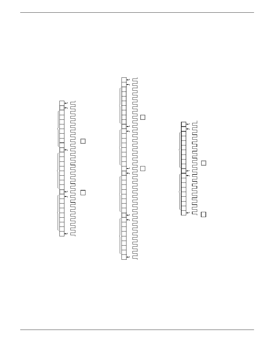
Serial Port Operation
The MIC284 uses standard SMBus Write_Byte and
Read_Byte operations for communication with its host. The
SMBus Write_Byte operation involves sending the device's
slave address (with the R/W bit low to signal a write opera-
tion), followed by a command byte and a data byte. The
SMBus Read_Byte operation is similar, but is a composite
write and read operation: the host first sends the device's
slave address followed by the command byte, as in a write
operation. A new start bit must then be sent to the MIC284,
followed by a repeat of the slave address with the R/W bit
(LSB) set to the high (read) state. The data to be read from
the part may then be clocked out.
The command byte is eight bits wide. This byte carries the
address of the MIC284 register to be operated upon, and is
stored in the part's pointer register. The pointer register is an
internal write-only register. The command byte (pointer
register) values corresponding to the various MIC284 regis-
ter addresses are shown in Table 2. Command byte values
other than those explicitly shown are reserved, and should
not be used. Any command byte sent to the MIC284 will
persist in the pointer register indefinitely until it is overwritten
by another command byte. If the location latched in the
pointer register from the last operation is known to be correct
(i.e., points to the desired register), then the Receive_Byte
procedure may be used. To perform a Receive_Byte, the host
sends an address byte to select the MIC284, and then
retrieves the data byte. Figures 1 through 3 show the formats
for these procedures.

MIC284
Micrel
MIC284
8
September 29, 2000
e
t
y
B
_
d
n
a
m
m
o
C
r
e
t
s
i
g
e
R
t
e
g
r
a
T
y
r
a
n
i
B
x
e
H
l
e
b
a
L
n
o
i
t
p
i
r
c
s
e
D
0
0
0
0
0
0
0
0
b
0
0
h
0
P
M
E
T
e
r
u
t
a
r
e
p
m
e
t
l
a
c
o
l
1
0
0
0
0
0
0
0
b
1
0
h
G
I
F
N
O
C
r
e
t
s
i
g
e
r
n
o
i
t
a
r
u
g
i
f
n
o
c
0
1
0
0
0
0
0
0
b
2
0
h
0
T
S
Y
H
_
T
s
i
s
e
r
e
t
s
y
h
e
r
u
t
a
r
e
p
m
e
t
l
a
c
o
l
1
1
0
0
0
0
0
0
b
3
0
h
0
T
E
S
_
T
t
n
i
o
p
t
e
s
e
r
u
t
a
r
e
p
m
e
t
l
a
c
o
l
0
0
0
0
1
0
0
0
b
0
1
h
1
P
M
E
T
e
r
u
t
a
r
e
p
m
e
t
e
t
o
m
e
r
0
1
0
0
1
0
0
0
b
2
1
h
1
T
S
Y
H
_
T
s
i
s
e
r
e
t
s
y
h
e
r
u
t
a
r
e
p
m
e
t
e
t
o
m
e
r
1
1
0
0
1
0
0
0
b
3
1
h
1
T
E
S
_
T
t
n
i
o
p
t
e
s
e
r
u
t
a
r
e
p
m
e
t
e
t
o
m
e
r
0
1
0
0
0
1
0
0
b
2
2
h
1
T
I
R
C
n
s
i
s
e
r
e
t
s
y
h
e
r
u
t
a
r
e
p
m
e
t
-
r
e
v
o
1
1
0
0
0
1
0
0
b
3
2
h
1
T
I
R
C
t
n
i
o
p
t
e
s
e
r
u
t
a
r
e
p
m
e
t
-
r
e
v
o
Table 2. MIC284 Register Addresses
September 29, 2000
9
MIC284
MIC284
Micrel
S
1001
XX
A
0
0
A
0
0
XXXXXXA
X
X
X
XXXX
X
/A
P
MIC284 Sla
v
e
Address
D
ATA
CLK
Command Byte
Data Byte to MIC284
ST
AR
T
ST
OP
R/W =
WRITE
A
CKNO
WLEDGE
A
CKNO
WLEDGE
NO
T A
CKNO
WLEDGE
Master-to-sla
v
e
tr
ansmission
Sla
v
e-to-master response
Figure 1. WRITE_BYTE Protocol
S
1001
XX
A
0
XX
A
0
0
A
0
0
XXXXXXAS
1
1
1
00
X
X
X
XXXX
A
X
/A
P
MIC284 Sla
v
e
Address
D
ATA
CLK
Command Byte
MIC284 Sla
v
e
Address
Data Read F
rom MIC284
ST
AR
T
ST
AR
T
ST
OP
R/W =
WRITE
R/W = READ
A
CKNO
WLEDGE
A
CKNO
WLEDGE
A
CKNO
WLEDGE
NO
T A
CKNO
WLEDGE
Master-to-sla
v
e
tr
ansmission
Sla
v
e-to-master response
Figure 2. READ_BYTE Protocol
S
1001
XX
A
0
1A
/
A
X
X
X
XXX
P
X
X
MIC284 Sla
v
e
Address
D
ATA
CLK
Data Byte from MIC284
ST
AR
T
ST
OP
R/W = READ
A
CKNO
WLEDGE
NO
T A
CKNO
WLEDGE
Master-to-sla
v
e
tr
ansmission
Sla
v
e-to-master response
Figure 3. RECEIVE_BYTE
MIC284
Micrel
MIC284
10
September 29, 2000
S
1001
XXX
AX
X
XXXXXXXA
MIC284 Sla
v
e
Address
First Byte of
T
r
ansaction
ST
AR
T
A
CKNO
WLEDGE
A
CKNO
WLEDGE
R/W = DONT CARE
/A
P
X
X
XXXXXX
Last Byte of
T
r
ansaction
A/D Con
v
e
r
ter
in Standb
y
Con
v
ersion
in Prog
ress
Ne
w Con
v
ersion
in Prog
ress
Ne
w Con
v
ersion
Begins
Con
v
ersion Interr
upted
By MIC284 Ac
kno
wledge
First
Result
Ready
t
CONV1
ST
OP
NO
T A
CKNO
WLEDGE
...
Master-to-sla
v
e
tr
ansmission
Sla
v
e-to-master response
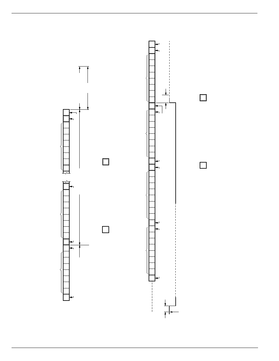
Figure 4. A/D Converter Timing
A
SS
1000
XX
A
0
XX
A
0
0
A
00000001
A
1
0
1
00
X
X
XXXXXX
/
A
P
MIC284 Sla
v
e
Address
T
emper
ature e
v
ent occurs
MIC284 Sla
v
e
Address
INT
Command Byte = 01
h
= CONFIG
CONFIG V
alue*
ST
AR
T
ST
AR
T
ST
OP
R/W =
WRITE
A
CKNO
WLEDGE
A
CKNO
WLEDGE
A
CKNO
WLEDGE
R/W = READ
NO
T A
CKNO
WLEDGE
Master-to-sla
v
e
tr
ansmission
Sla
v
e-to-master response
t
n/INT
t
/INT
*
Status bits in CONFIG are cleared to z
ero f
ollo
wing this oper
ation
Figure 5. Responding to Interrupts

September 29, 2000
11
MIC284
MIC284
Micrel
e
r
u
t
a
r
e
p
m
e
T
y
r
a
n
i
B
x
e
H
C
∞
5
2
1
+
1
0
1
1
1
1
1
0
b
D
7
h
C
∞
5
2
+
1
0
0
1
1
0
0
0
b
9
1
h
C
∞
0
.
1
+
1
0
0
0
0
0
0
0
b
1
0
h
C
∞
0
0
0
0
0
0
0
0
0
b
0
0
h
C
∞
0
.
1
≠
1
1
1
1
1
1
1
1
b
F
F
h
C
∞
5
2
≠
1
1
1
0
0
1
1
1
b
7
E
h
C
∞
0
4
≠
0
0
0
1
1
0
1
1
b
8
D
h
C
∞
5
5
≠
1
0
0
1
0
0
1
1
b
9
C
h
Table 3. Digital Temperature Format
Temperature Data Format
The LSB of each register represents one degree Centigrade.
The values are in a two's complement format, wherein the
most significant bit (D7), represents the sign: zero for positive
temperatures and one for negative temperatures. Table 3
shows examples of the data format used by the MIC284 for
temperatures.
A/D Converter Timing
Whenever the MIC284 is not in its low power shutdown mode,
the internal A/D converter (ADC) attempts to make continu-
ous conversions unless interrupted by a bus transaction
accessing the MIC284. When the part is accessed, the
conversion in progress will be halted, and the partial result
discarded. When the access to the MIC284 is complete, the
ADC will begin a new conversion cycle with results for the
remote zone valid t
CONV1
after that, and for the local zone
t
CONV0
later. Figure 4 shows this behavior. The conversion
time is twice as long for external conversions as it is for
internal conversions. This allows the use of a filter capacitor
on T1 without a loss of accuracy due to the resulting longer
settling times.
Upon powering-up, coming out of shutdown mode, or resum-
ing operation following a serial bus transaction, the ADC will
begin acquiring temperature data starting with the external
zone (zone 1), followed by the internal zone (zone 0). If the
ADC is interrupted by a serial bus transaction, it will restart the
conversion that was interrupted and then continue in the
normal sequence. This sequence will repeat indefinitely until
the MIC284 is shut down, powered off, or is interrupted by a
serial bus transaction as described above.
Power-On
When power is initially applied, the MIC284's internal regis-
ters are set to their default states, and A0 is read to establish
the device's slave address. The MIC284's power-up default
state can be summarized as follows:
∑ Normal Mode operation (i.e., part is not in shut-
down)
∑ /INT function is set to Comparator Mode
∑ Fault Queue depth = 1 (FQ=00)
∑ Interrupts are enabled (IM = 0)
∑ T_SET0 = 81
∞C; T_HYST0 = 76∞C
∑ T_SET1 = 97
∞C; T_HYST1 = 92∞C
∑ CRIT1 = 97
∞C; nCRIT1 = 92∞C
∑ Initialized to recognize overtemperature faults
Comparator and Interrupt Modes
Depending on the setting of the MODE bit in the configuration
register, the /INT output will behave either as an interrupt
request signal or a thermostatic control signal. Thermostatic
operation is known as
comparator mode. The /INT output is
asserted when the measured temperature, as reported in
either of the TEMPx registers, exceeds the threshold pro-
grammed into the corresponding T_SETx register for the
number of conversions specified by Fault_Queue (described
below). In comparator mode, /INT will remain asserted and
the status bits will remain high unless and until the measured
temperature falls below the value in the T_HYSTx register for
Fault_Queue conversions. No action on the part of the host
is required for operation in comparator mode. Note that
entering shutdown mode will not affect the state of /INT when
the device is in comparator mode.
In
interrupt mode, once a temperature event has caused a
status bit (Sx) to be set, and the /INT output to be asserted,
they will not be automatically de-asserted when the mea-
sured temperature falls below T_HYSTx. They can only be
de-asserted by reading any of the MIC284's internal registers
or by putting the device into shutdown mode. If the most
recent temperature event was an overtemperature condition,
Sx will not be set again, and /INT cannot be reasserted, until
the device has detected that TEMPx < T_HYSTx. Similarly,
if the most recent temperature event was an undertemperature
condition, Sx will not be set again, and /INT cannot be
reasserted, until the device has detected that TEMPx >
T_SETx. This keeps the internal logic of the MIC284 back-
ward compatible with that of the LM75 and similar devices. In
both modes, the MIC284 will be responsive to over-tempera-
ture events at power-up. See "Interrupt Generation", below.
Shutdown Mode
Setting the SHDN bit in the configuration register halts the
otherwise continuous conversions by the A/D converter. The
MIC284's power consumption drops to 1
µA typical in shut-
down mode. All registers may be read from or written to while
in shutdown mode. Serial bus activity will slightly increase the
part's power consumption.
Entering shutdown mode will not affect the state of /INT when
the device is in comparator mode (MODE = 0). It will retain
its state until after the device exits shutdown mode and
resumes A/D conversions.

MIC284
Micrel
MIC284
12
September 29, 2000
If the device is shut down while in interrupt mode (mode = 1),
the /INT pin will be unconditionally de-asserted and the
internal latches holding the interrupt status will be cleared.
Therefore, no interrupts will be generated while the MIC284
is in shutdown mode, and the interrupt status will not be
retained. Regardless of the setting of the MODE bit, the state
of /CRIT and its corresponding status bit, CRIT1, does not
change when the MIC284 enters shutdown mode. They will
retain their states until after the device exits shutdown mode
and resumes A/D conversions. Since entering shutdown
mode stops A/D conversions, the MIC284 is incapable of
detecting or reporting temperature events of any kind while in
shutdown. Diode fault detection requires one or more A/D
conversion cycles to detect external sensor faults, therefore
diode faults will not be reported until the MIC284 exits
shutdown (see "Diode Faults" above).
Fault Queues
Fault queues (programmable digital filters) are provided in
the MIC284 to prevent false tripping due to thermal or
electrical noise. The two bits in CONFIG[4:3] set the depth of
Fault_Queue. Fault_Queue then determines the number of
consecutive temperature events (TEMPx > T_SETx, TEMPx
< T_HYSTx, TEMP1 > CRIT1, or TEMP1 < nCRIT1) which
must occur in order for the condition to be considered valid.
There are separate fault queues for each zone and for the
over-temperature detect function. As an example, assume
the part is in comparator mode, and CONFIG[4:3] is pro-
grammed with 10
b
. The measured temperature in zone one
would have to exceed T_SET1 for four consecutive A/D
conversions before /INT would be asserted or the S1 status
bit set. Similarly, TEMP1 would have to be less than T_HYST1
for four consecutive conversions before /INT would be reset.
Like any filter, the fault queue function also has the effect of
delaying the detection of temperature events. In this ex-
ample, it would take 4 x t
CONV
to detect a temperature event.
The depth of Fault_Queue vs. D[4:3] of the configuration
register is shown in Table 4:
]
3
:
4
[
G
I
F
N
O
C
h
t
p
e
D
e
u
e
u
Q
_
t
l
u
a
F
0
0
*
n
o
i
s
r
e
v
n
o
c
1
1
0
s
n
o
i
s
r
e
v
n
o
c
2
0
1
s
n
o
i
s
r
e
v
n
o
c
4
1
1
s
n
o
i
s
r
e
v
n
o
c
6
g
n
i
t
t
e
s
t
l
u
a
f
e
D
*
Table 4. Fault_Queue Depth Settings
Interrupt Generation
Assuming the MIC284 is in interrupt mode and interrupts are
enabled, there are five different conditions that will cause the
MIC284 to set one of the status bits (S0, S1, or CRIT1) in
CONFIG and assert the /INT output and/or the /CRIT output.
These conditions are listed in Table 5. When a temperature
event occurs, the corresponding status bit will be set in
CONFIG. This action cannot be masked. However, a
temperature event will only generate an interrupt signal on /
INT if it is specifically enabled by the interrupt mask bit (IM =0
in the configuration register). Following an interrupt, the host
should read the contents of the configuration register to
confirm that the MIC284 was the source of the interrupt. A
read operation on
any register will cause /INT to be de-
asserted. This is shown in Figure 5. The status bits will be
cleared once CONFIG has been read.
Since temperature-to-digital conversions continue while /INT
is asserted, the measured temperature could change be-
tween the MIC284's assertion of /INT or /CRIT and the host's
response. It is good practice for the interrupt service routine
to read the value in TEMPx, to verify that the over-tempera-
ture or under-temperature condition still exists. In addition,
more than one temperature event may have occurred simul-
taneously or in rapid succession between the assertion of
/INT and servicing of the MIC284 by the host. The interrupt
service routine should allow for this eventuality. Keep in mind
that clearing the status bits and deasserting /INT is
not
sufficient to allow further interrupts to occur. TEMPx must
become less than T_HYSTx if the last event was an over-
temperature condition, or greater than T_SETx if the last
event was an under-temperature condition, before /INT can
be asserted again.
Putting the device into shutdown mode will de-assert /INT
and clear the S0 and S1 status bits. This should not be done
before completing the appropriate interrupt service routine(s).
/CRIT Output
If and when the measured remote temperature exceeds the
value programmed into the CRIT1 register, the /CRIT output
will be asserted and CRIT1 in the configuration register will be
set. If and when the measured temperature in zone one
subsequently falls below the value programmed into nCRIT1,
the /CRIT output will be de-asserted and the CRIT1 bit in
CONFIG will be cleared. This action cannot be masked and
is completely independent of the settings of the mode bit and
interrupt mask bit. The host may poll the state of the /CRIT
output at any time by reading the configuration register. The
state of the CRIT1 bit exactly follows the state of the /CRIT
output. The states of /CRIT and CRIT1 do not change when
the MIC284 enters shutdown mode. Entering shutdown mode
stops A/D conversions, however, so their states will not
change while the device is shut down.
Polling
The MIC284 may either be polled by the host, or request the
host's attention via the /INT pin. In the case of polled
operation, the host periodically reads the contents of CONFIG
to check the state of the status bits. The act of reading
CONFIG clears the status bits. If more than one event that
sets a given status bit occurs before the host polls the
MIC284, only the fact that at least one such event has
occurred will be apparent to the host. For polled systems, the
interrupt mask bit should be set (IM = 1). This will disable
interrupts from the MIC284, and prevent the /INT pin from
sinking current. The host may poll the state of the /CRIT
output at any time by reading the configuration register. The
state of the CRIT1 bit exactly follows the state of the /CRIT
output.

September 29, 2000
13
MIC284
MIC284
Micrel
T
N
E
V
E
*
N
O
I
T
I
D
N
O
C
*
*
e
s
n
o
p
s
e
R
4
8
2
C
I
M
e
t
o
m
e
r
,
e
r
u
t
a
r
e
p
m
e
t
h
g
i
H
1
T
E
S
_
T
>
1
P
M
E
T
T
N
I
/
t
r
e
s
s
a
,
G
I
F
N
O
C
n
i
1
S
t
e
S
l
a
c
o
l
,
e
r
u
t
a
r
e
p
m
e
t
h
g
i
H
0
T
E
S
_
T
>
0
P
M
E
T
T
N
I
/
t
r
e
s
s
a
,
G
I
F
N
O
C
n
i
0
S
t
e
S
e
t
o
m
e
r
,
e
r
u
t
a
r
e
p
m
e
t
w
o
L
1
T
S
Y
H
_
T
<
1
P
M
E
T
T
N
I
/
t
r
e
s
s
a
,
G
I
F
N
O
C
n
i
1
S
t
e
S
l
a
c
o
l
,
e
r
u
t
a
r
e
p
m
e
t
w
o
L
0
T
S
Y
H
_
T
<
0
P
M
E
T
T
N
I
/
t
r
e
s
s
a
,
G
I
F
N
O
C
n
i
0
S
t
e
S
e
t
o
m
e
r
,
e
r
u
t
a
r
e
p
m
e
t
-
r
e
v
O
1
T
I
R
C
>
1
P
M
E
T
T
I
R
C
/
t
r
e
s
s
a
,
G
I
F
N
O
C
n
i
T
I
R
C
t
e
S
e
t
o
m
e
r
,
e
r
u
t
a
r
e
p
m
e
t
-
r
e
v
O
T
O
N
1
T
I
R
C
n
<
P
M
E
T
T
I
R
C
/
t
r
e
s
s
a
-
e
d
,
G
I
F
N
O
C
n
i
T
I
R
C
r
a
e
l
C
t
l
u
a
F
e
d
o
i
D
D
N
G
r
o
D
D
V
o
t
d
e
t
r
o
h
s
1
T
r
o
n
e
p
o
1
T
T
N
I
/
t
r
e
s
s
a
,
G
I
F
N
O
C
n
i
1
S
d
n
a
T
I
R
C
t
e
S
*
*
*
T
I
R
C
/
d
n
a
d
e
z
i
n
g
o
c
e
r
e
b
o
t
s
n
o
i
s
r
e
v
n
o
c
e
u
e
u
Q
_
t
l
u
a
F
r
o
f
e
u
r
t
e
b
t
s
u
m
N
O
I
T
I
D
N
O
C
*
d
e
l
b
a
n
e
s
t
p
u
r
e
t
n
i
s
e
m
u
s
s
A
*
*
F
7
=
C
∞
7
2
1
+
n
a
h
t
s
s
e
l
e
u
l
a
v
y
n
a
o
t
t
e
s
e
r
a
1
T
I
R
C
d
n
a
1
T
E
S
_
T
t
a
h
t
s
e
m
u
s
s
A
*
*
*
h
1
1
1
1
1
1
1
0
=
b
.
Table 5. MIC284 Temperature Events

MIC284
Micrel
MIC284
14
September 29, 2000
Register Set and Programmer's Model
Internal Register Set
e
m
a
N
n
o
i
t
p
i
r
c
s
e
D
e
t
y
B
d
n
a
m
m
o
C
n
o
i
t
a
r
e
p
O
t
l
u
a
f
e
D
p
U
-
r
e
w
o
P
0
P
M
E
T
e
r
u
t
a
r
e
p
m
e
t
l
a
c
o
l
0
0
h
y
l
n
o
d
a
e
r
t
i
b
-
8
0
0
h
)
C
∞
0
(
)
1
(
G
I
F
N
O
C
r
e
t
s
i
g
e
r
n
o
i
t
a
r
u
g
i
f
n
o
c
1
0
h
e
t
i
r
w
/
d
a
e
r
t
i
b
-
8
0
0
h
)
2
(
0
T
S
Y
H
_
T
s
i
s
e
r
e
t
s
y
h
l
a
c
o
l
2
0
h
e
t
i
r
w
/
d
a
e
r
t
i
b
-
8
C
4
h
)
C
∞
6
7
+
(
0
T
E
S
_
T
t
n
i
o
p
t
e
s
e
r
u
t
a
r
e
p
m
e
t
l
a
c
o
l
3
0
h
e
t
i
r
w
/
d
a
e
r
t
i
b
-
8
1
5
h
)
C
∞
1
8
+
(
1
P
M
E
T
e
r
u
t
a
r
e
p
m
e
t
e
t
o
m
e
r
0
1
h
y
l
n
o
d
a
e
r
t
i
b
-
8
0
0
h
)
C
∞
0
(
)
1
(
1
T
S
Y
H
_
T
s
i
s
e
r
e
t
s
y
h
e
t
o
m
e
r
2
1
h
e
t
i
r
w
/
d
a
e
r
t
i
b
-
8
C
5
h
)
C
∞
2
9
+
(
1
T
E
S
_
T
e
r
u
t
a
r
e
p
m
e
t
e
t
o
m
e
r
t
n
i
o
p
t
e
s
3
1
h
e
t
i
r
w
/
d
a
e
r
t
i
b
-
8
1
6
h
)
C
∞
7
9
+
(
1
T
I
R
C
n
e
r
u
t
a
r
e
p
m
e
t
-
r
e
v
o
s
i
s
e
r
e
t
s
y
h
2
2
h
e
t
i
r
w
/
d
a
e
r
t
i
b
-
8
C
5
h
)
C
∞
2
9
+
(
1
T
I
R
C
e
r
u
t
a
r
e
p
m
e
t
-
r
e
v
o
t
n
i
o
p
t
e
s
e
r
u
t
a
r
e
p
m
e
t
3
2
h
e
t
i
r
w
/
d
a
e
r
t
i
b
-
8
1
6
h
)
C
∞
7
9
+
(
(1)
TEMP0 and TEMP1 will contain measured temperature data after the completion of one conversion cycle.
(2)
After the first Fault_Queue conversions are complete, status bits will be set if TEMPx > T_SETx or TEMP1 > CRIT1.
Detailed Register Descriptions
Configuration Register
)
G
I
F
N
O
C
(
R
E
T
S
I
G
E
R
N
O
I
T
A
R
U
G
I
F
N
O
C
e
t
i
r
W
/
d
a
e
R
t
i
B
-
8
]
7
[
D
]
6
[
D
]
5
[
D
]
4
[
D
]
3
[
D
]
2
[
D
]
1
[
D
]
0
[
D
y
l
n
o
d
a
e
r
y
l
n
o
d
a
e
r
y
l
n
o
d
a
e
r
e
t
i
r
w
/
d
a
e
r
e
t
i
r
w
/
d
a
e
r
e
t
i
r
w
/
d
a
e
r
e
t
i
r
w
/
d
a
e
r
l
a
c
o
l
s
u
t
a
t
s
)
0
S
(
e
t
o
m
e
r
s
u
t
a
t
s
)
1
S
(
T
I
R
C
/
s
u
t
a
t
s
)
1
T
I
R
C
(
e
u
e
u
q
t
l
u
a
f
h
t
p
e
d
)
]
0
:
1
[
Q
F
(
t
p
u
r
r
e
t
n
i
k
s
a
m
)
M
I
(
T
N
I
/
P
M
C
e
d
o
m
)
E
D
O
M
(
n
w
o
d
t
u
h
S
)
N
D
H
S
(
s
t
i
B
n
o
i
t
c
n
u
F
n
o
i
t
a
r
e
p
O
0
S
)
y
l
n
o
d
a
e
r
(
s
u
t
a
t
s
t
p
u
r
r
e
t
n
i
l
a
c
o
l
t
n
e
v
e
o
n
=
0
,
d
e
r
u
c
c
o
t
n
e
v
e
=
1
1
S
)
y
l
n
o
d
a
e
r
(
s
u
t
a
t
s
t
p
u
r
r
e
t
n
i
e
t
o
m
e
r
t
n
e
v
e
o
n
=
0
,
d
e
r
u
c
c
o
t
n
e
v
e
=
1
1
T
I
R
C
)
y
l
n
o
d
a
e
r
(
s
u
t
a
t
s
e
r
u
t
a
r
e
p
m
e
t
-
r
e
v
o
e
t
o
m
e
r
t
n
e
v
e
o
n
=
0
,
e
r
u
t
a
r
e
p
m
e
t
-
r
e
v
o
=
1
]
0
:
1
[
Q
F
h
t
p
e
d
e
u
e
u
Q
_
t
l
u
a
F
,
s
n
o
i
s
r
e
v
n
o
c
2
=
1
0
,
n
o
i
s
r
e
v
n
o
c
1
=
0
0
s
n
o
i
s
r
e
v
n
o
c
6
=
1
1
,
s
n
o
i
s
r
e
v
n
o
c
4
=
0
1
M
I
k
s
a
m
t
p
u
r
r
e
t
n
i
d
e
l
b
a
n
e
s
t
p
u
r
r
e
t
n
i
=
0
,
d
e
l
b
a
s
i
d
=
1
E
D
O
M
t
p
u
r
r
e
t
n
i
/
r
o
t
a
r
a
p
m
o
c
n
i
p
T
N
I
/
r
o
f
n
o
i
t
c
e
l
e
s
e
d
o
m
,
e
d
o
m
t
p
u
r
r
e
t
n
i
=
1
e
d
o
m
r
o
t
a
r
a
p
m
o
c
=
0
N
D
H
S
n
w
o
d
t
u
h
s
/
l
a
m
r
o
n
n
o
i
t
c
e
l
e
s
e
d
o
m
g
n
i
t
a
r
e
p
o
,
n
w
o
d
t
u
h
s
=
1
l
a
m
r
o
n
=
0
CONFIG Power-Up Value: 0000 0000
b
= 00
h
(*)
∑ not in shutdown mode
∑ comparator mode
∑ /INT = active low
∑ Fault_Queue depth = 1
∑ interrupts enabled.
∑ no temperature events pending
CONFIG Command Byte Value: 0000 0001
b
= 01
h
* Following the first Fault_Queue conversions, one or more of the status bits may be set.

September 29, 2000
15
MIC284
MIC284
Micrel
T_SET0 Power-Up Value: 0101 0001
b
= 51
h
(+81
∞C)
T_SET0 Command Byte Value: 0000 0011
b
= 03
h
* Each LSB represents one degree Centigrade. The values are
in a two's complement format such that 0
∞C is reported as
0000 0000
b
. See "Temperature Data Format" for more details.
Local Temperature Setpoint Register
)
0
T
E
S
_
T
(
T
N
I
O
P
T
E
S
E
R
U
T
A
R
E
P
M
E
T
L
A
C
O
L
e
t
i
r
W
/
d
a
e
R
t
i
B
-
8
]
7
[
D
]
6
[
D
]
5
[
D
]
4
[
D
]
3
[
D
]
2
[
D
]
1
[
D
]
0
[
D
B
S
M
6
t
i
b
5
t
i
b
4
t
i
b
3
t
i
b
2
t
i
b
1
t
i
b
B
S
L
t
n
i
o
p
t
e
s
e
r
u
t
a
r
e
p
m
e
t
l
a
c
o
l
s
t
i
B
n
o
i
t
c
n
u
F
n
o
i
t
a
r
e
p
O
]
0
:
7
[
D
*
t
n
i
o
p
t
e
s
e
r
u
t
a
r
e
p
m
e
t
l
a
c
o
l
e
t
i
r
w
/
d
a
e
r
T_HYST0 Power-Up Value: 0100 1100
b
= 4C
h
(+76
∞C)
T_HYST0 Command Byte Value: 0000 0010
b
= 02
h
* Each LSB represents one degree Centigrade. The values are
in a two's complement format such that 0
∞C is reported as
0000 0000
b
. See "Temperature Data Format" for more details.
Local Temperature Hysteresis Register
)
0
T
S
Y
H
_
T
(
S
I
S
E
R
E
T
S
Y
H
E
R
U
T
A
R
E
P
M
E
T
L
A
C
O
L
e
t
i
r
W
/
d
a
e
R
t
i
B
-
8
]
7
[
D
]
6
[
D
]
5
[
D
]
4
[
D
]
3
[
D
]
2
[
D
]
1
[
D
]
0
[
D
B
S
M
6
t
i
b
5
t
i
b
4
t
i
b
3
t
i
b
2
t
i
b
1
t
i
b
B
S
L
g
n
i
t
t
e
s
s
i
s
e
r
e
t
s
y
h
e
r
u
t
a
r
e
p
m
e
t
l
a
c
o
l
s
t
i
B
n
o
i
t
c
n
u
F
n
o
i
t
a
r
e
p
O
]
0
:
7
[
D
*
g
n
i
t
t
e
s
s
i
s
e
r
e
t
s
y
h
e
r
u
t
a
r
e
p
m
e
t
l
a
c
o
l
e
t
i
r
w
/
d
a
e
r
Local Temperature Result Register
)
0
P
M
E
T
(
S
T
L
U
S
E
R
E
R
U
T
A
R
E
P
M
E
T
L
A
C
O
L
y
l
n
O
d
a
e
R
t
i
B
-
8
]
7
[
D
]
6
[
D
]
5
[
D
]
4
[
D
]
3
[
D
]
2
[
D
]
1
[
D
]
0
[
D
B
S
M
6
t
i
b
5
t
i
b
4
t
i
b
3
t
i
b
2
t
i
b
1
t
i
b
B
S
L
*
C
D
A
m
o
r
f
a
t
a
d
e
r
u
t
a
r
e
p
m
e
t
l
a
c
o
l
s
t
i
B
n
o
i
t
c
n
u
F
n
o
i
t
a
r
e
p
O
]
0
:
7
[
D
l
a
c
o
l
e
h
t
r
o
f
a
t
a
d
e
r
u
t
a
r
e
p
m
e
t
d
e
r
u
s
a
e
m
*
e
n
o
z
y
l
n
o
d
a
e
r
TEMP0 Power-Up Value: 0000 0000
b
= 00
h
(0
∞C)
TEMP0 Command Byte Value: 0000 0000
b
= 00
h
* Each LSB represents one degree Centigrade. The values are
in a two's complement format such that 0
∞C is reported as
0000 0000
b
. See "Temperature Data Format" for more details.
TEMP0 will contain measured temperature data after the
completion of one conversion.

MIC284
Micrel
MIC284
16
September 29, 2000
T_SET1 Power-Up Value: 0110 0001
b
= 61
h
(+97
∞C)
T_SET1 Command Byte Value: 0001 0011
b
= 13
h
* Each LSB represents one degree Centigrade. The values are
in a two's complement format such that 0
∞C is reported as
0000 0000
b
. See "Temperature Data Format" for more details.
Remote Temperature Setpoint Register
)
1
T
E
S
_
T
(
T
N
I
O
P
T
E
S
E
R
U
T
A
R
E
P
M
E
T
E
T
O
M
E
R
e
t
i
r
W
/
d
a
e
R
t
i
B
-
8
]
7
[
D
]
6
[
D
]
5
[
D
]
4
[
D
]
3
[
D
]
2
[
D
]
1
[
D
]
0
[
D
B
S
M
6
t
i
b
5
t
i
b
4
t
i
b
3
t
i
b
2
t
i
b
1
t
i
b
B
S
L
t
n
i
o
p
t
e
s
e
r
u
t
a
r
e
p
m
e
t
e
t
o
m
e
r
s
t
i
B
n
o
i
t
c
n
u
F
n
o
i
t
a
r
e
p
O
]
0
:
7
[
D
*
t
n
i
o
p
t
e
s
e
r
u
t
a
r
e
p
m
e
t
e
t
o
m
e
r
e
t
i
r
w
/
d
a
e
r
T_HYST1 Power-Up Value: 0101 1100
b
= 5C
h
(+92
∞C)
T_HYST1 Command Byte Value: 0001 0010
b
= 12
h
* Each LSB represents one degree Centigrade. The values are
in a two's complement format such that 0
∞C is reported as
0000 0000
b
. See "Temperature Data Format" for more details.
Remote Temperature Hysteresis Register
)
1
T
S
Y
H
_
T
(
S
I
S
E
R
E
T
S
Y
H
E
R
U
T
A
R
E
P
M
E
T
E
T
O
M
E
R
e
t
i
r
W
/
d
a
e
R
t
i
B
-
8
]
7
[
D
]
6
[
D
]
5
[
D
]
4
[
D
]
3
[
D
]
2
[
D
]
1
[
D
]
0
[
D
B
S
M
6
t
i
b
5
t
i
b
4
t
i
b
3
t
i
b
2
t
i
b
1
t
i
b
B
S
L
g
n
i
t
t
e
s
s
i
s
e
r
e
t
s
y
h
e
r
u
t
a
r
e
p
m
e
t
e
t
o
m
e
r
s
t
i
B
n
o
i
t
c
n
u
F
n
o
i
t
a
r
e
p
O
]
0
:
7
[
D
*
g
n
i
t
t
e
s
s
i
s
e
r
e
t
s
y
h
e
r
u
t
a
r
e
p
m
e
t
e
t
o
m
e
r
e
t
i
r
w
/
d
a
e
r
Remote Temperature Result Register
)
1
P
M
E
T
(
T
L
U
S
E
R
E
R
U
T
A
R
E
P
M
E
T
E
T
O
M
E
R
y
l
n
O
d
a
e
R
t
i
B
-
8
]
7
[
D
]
6
[
D
]
5
[
D
]
4
[
D
]
3
[
D
]
2
[
D
]
1
[
D
]
0
[
D
B
S
M
6
t
i
b
5
t
i
b
4
t
i
b
3
t
i
b
2
t
i
b
1
t
i
b
B
S
L
*
C
D
A
m
o
r
f
a
t
a
d
e
r
u
t
a
r
e
p
m
e
t
e
t
o
m
e
r
s
t
i
B
n
o
i
t
c
n
u
F
n
o
i
t
a
r
e
p
O
]
0
:
7
[
D
e
t
o
m
e
r
e
h
t
r
o
f
a
t
a
d
e
r
u
t
a
r
e
p
m
e
t
d
e
r
u
s
a
e
m
*
e
n
o
z
y
l
n
o
d
a
e
r
TEMP1 Power-Up Value: 0000 0000
b
= 00
h
(0
∞C)
TEMP1 Command Byte Value: 0001 0000
b
= 10
h
* Each LSB represents one degree Centigrade. The values are
in a two's complement format such that 0
∞C is reported as
0000 0000
b
. See "Temperature Data Format" for more details.
TEMP1 will contain measured temperature data for the
selected zone after the completion of one conversion.

September 29, 2000
17
MIC284
MIC284
Micrel
CRIT1 Power-Up Value: 0110 0001
b
= 61
h
(+97
∞C)
CRIT1 Command Byte Value: 0010 0011b = 23
h
* Each LSB represents one degree Centigrade. The values are
in a two's complement format such that 0
∞C is reported as
0000 0000
b
. See "Temperature Data Format" for more details.
Remote Over-Temperature Setpoint Register
)
1
T
I
R
C
(
T
N
I
O
P
T
E
S
E
R
U
T
A
R
E
P
M
E
T
-
R
E
V
O
E
T
O
M
E
R
e
t
i
r
W
/
d
a
e
R
t
i
B
-
8
]
7
[
D
]
6
[
D
]
5
[
D
]
4
[
D
]
3
[
D
]
2
[
D
]
1
[
D
]
0
[
D
B
S
M
6
t
i
b
5
t
i
b
4
t
i
b
3
t
i
b
2
t
i
b
1
t
i
b
B
S
L
t
n
i
o
p
t
e
s
e
r
u
t
a
r
e
p
m
e
t
-
r
e
v
o
e
t
o
m
e
r
s
t
i
B
n
o
i
t
c
n
u
F
n
o
i
t
a
r
e
p
O
]
0
:
7
[
D
*
t
n
i
o
p
t
e
s
e
r
u
t
a
r
e
p
m
e
t
-
r
e
v
o
e
t
o
m
e
r
e
t
i
r
w
/
d
a
e
r
Remote Over-Temperature Hysteresis Register
)
1
T
I
R
C
n
(
S
I
S
E
R
E
T
S
Y
H
E
R
U
T
A
R
E
P
M
E
T
-
R
E
V
O
E
T
O
M
E
R
e
t
i
r
W
/
d
a
e
R
t
i
B
-
8
]
7
[
D
]
6
[
D
]
5
[
D
]
4
[
D
]
3
[
D
]
2
[
D
]
1
[
D
]
0
[
D
B
S
M
6
t
i
b
5
t
i
b
4
t
i
b
3
t
i
b
2
t
i
b
1
t
i
b
B
S
L
g
n
i
t
t
e
s
s
i
s
e
r
e
t
s
y
h
e
r
u
t
a
r
e
p
m
e
t
-
r
e
v
o
e
t
o
m
e
r
s
t
i
B
n
o
i
t
c
n
u
F
n
o
i
t
a
r
e
p
O
]
0
:
7
[
D
*
g
n
i
t
t
e
s
s
i
s
e
r
e
t
s
y
h
e
r
u
t
a
r
e
p
m
e
t
e
t
o
m
e
r
e
t
i
r
w
/
d
a
e
r
nCRIT Power-Up Value: 0101 1100
b
= 5C
h
(+92
∞C)
nCRIT1 Command Byte Value: 0010 0010
b
= 22
h
* Each LSB represents one degree Centigrade. The values are
in a two's complement format such that 0
∞C is reported as
0000 0000
b
. See "Temperature Data Format" for more details.

MIC284
Micrel
MIC284
18
September 29, 2000
Applications
Remote Diode Selection
Most small-signal PNP transistors with characteristics similar
to the JEDEC 2N3906 will perform well as remote tempera-
ture sensors. Table 6 lists several examples of such parts
that Micrel has tested for use with the MIC284. Other
transistors equivalent to these should also work well.
Minimizing Errors
Self-Heating
One concern when using a part with the temperature accu-
racy and resolution of the MIC284 is to avoid errors induced
by self-heating (V
DD
◊ I
DD
) + (V
OL
◊ I
OL
). In order to
understand what level of error this might represent, and how
to reduce that error, the dissipation in the MIC284 must be
calculated and its effects reduced to a temperature offset.
The worst-case operating condition for the MIC284 is when
V
DD
= 5.5V, MSOP-08 package. T he maximum power
dissipated in the part is given in Equation 1 below.
In most applications, the /INT output will be low for at most a
few milliseconds before the host resets it back to the high
state, making its duty cycle low enough that its contribution to
self-heating of the MIC284 is negligible. Similarly, the DATA
pin will in all likelihood have a duty cycle of substantially below
25% in the low state. These considerations, combined with
more typical device and application parameters, give a better
system-level view of device self-heating in interrupt-mode
usage. This is illustrated by Equation 2.
If the part is to be used in comparator mode, calculations
similar to those shown in Equation 2 (accounting for the
expected value and duty cycle of I
OL(/INT)
and I
OL(/CRIT)
)
will give a good estimate of the device's self-heating error.
In any application, the best test is to verify performance
against calculation in the final application environment. This
is especially true when dealing with systems for which some
Vendor
Part Number
Package
Fairchild
MMBT3906
SOT-23
On Semiconductor
MMBT3906L
SOT-23
Phillips Semiconductor
PMBT3906
SOT-23
Samsung
KST3906-TF
SOT-23
Table 6. Transistors Suitable for Remote Temperature Sensing Use
of the thermal data (e.g., PC board thermal conductivity and
ambient temperature) may be poorly defined or unobtainable
except by empirical means.
Series Resistance
The operation of the MIC284 depends upon sensing the
V
CB-E
of a diode-connected PNP transistor ("diode") at two
different current levels. For remote temperature measure-
ments, this is done using an external diode connected be-
tween T1 and ground.
Since this technique relies upon measuring the relatively
small voltage difference resulting from two levels of current
through the external diode, any resistance in series with the
external diode will cause an error in the temperature reading
from the MIC284. A good rule of thumb is this: for each ohm
in series with the external transistor, there will be a 0.9
∞C error
in the MIC284's temperature measurement. It isn't difficult to
keep the series resistance well below an ohm (typically <
0.1
), so this will rarely be an issue.
Filter Capacitor Selection
It is sometimes desirable to use a filter capacitor between the
T1 and GND pins of the MIC284. The use of this capacitor is
recommended in environments with a lot of high frequency
noise (such as digital switching noise), or if long wires are
used to attach to the remote diode. The maximum recom-
mended total capacitance from the T1 pin to GND is 2700pF.
This typically suggests the use of a 2200pF NP0 or C0G
ceramic capacitor with a 10% tolerance.
If the remote diode is to be at a distance of more than
6" --
12" from the MIC284, using twisted pair wiring or shielded
microphone cable for the connections to the diode can
significantly help reduce noise pickup. If using a long run of
shielded cable, remember to subtract the cable's conductor-
to-shield capacitance from the 2700pF maximum total ca-
pacitance.
P
[(I
V
) (I
V
) (I
V
) (I
V
)]
P
[(0.75mA
5.5V) + (6mA
0.8V) + (6mA
0.8V) + (6mA
0.8V)
P
18.53mW
R
of MSOP - 08 package is 206 C / W
Maximum T relative to T due to self heating is 18.53mW 206 C / W = 3.82 C
D
DD
DD
OL(DATA)
OL(DATA)
OL(/INT)
OL(/INT)
OL(/CRIT)
OL(/CRIT)
D
D
(j-a)
J
A
=
◊
+
◊
+
◊
+
◊
=
◊
◊
◊
◊
=
∞
◊
∞
∞
Equation 1. Worst-case self-heating
[(0.35mA I
3.3V) (25% 1.5mA I
0.3V) (1% 1.5mA I
0.3V) + (25% 1.5mA I
0.3V) = 1.38mW
T
(1.38mW
206 C / W)
DD(typ)
OL(DATA)
OL(/INT)
OL(/CRIT)
J
◊
+
◊
◊
+
◊
◊
◊
◊
=
◊
∞
=
∞
0.29 C
Equation 2. Real-world self-heating example
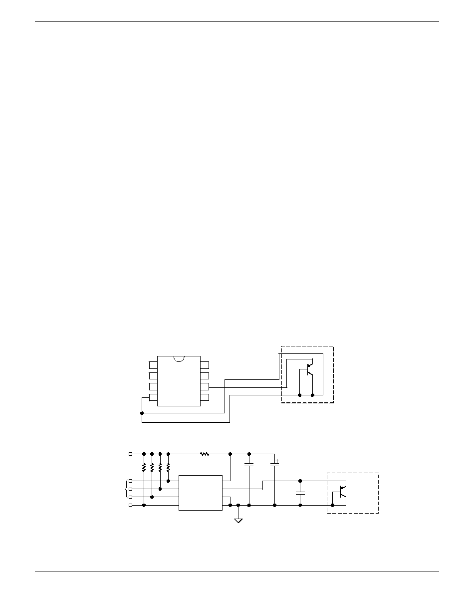
September 29, 2000
19
MIC284
MIC284
Micrel
REMOTE DIODE (T1)
GUARD/RETURN
1
2
3
DATA
CLK
/INT
GND
8
7
6
5
4
VDD
A0
T1
/CRIT
GUARD/RETURN
MIC284
Figure 6. Guard Traces/Kelvin Ground Returns
CLK
FROM
SERIAL BUS
HOST
OVER-TEMP
SHUTDOWN
Remote
Diode
2200pF
MIC284
/INT
/CRIT
DATA
100
3.3V
10k pull-ups
VDD
T1
A0
GND
4.7
µF
0.1
µF
Figure 7. V
DD
Decoupling for Very Noisy Supplies
Layout Considerations
The following guidelines should be kept in mind when design-
ing and laying out circuits using the MIC284:
1. Place the MIC284 as close to the remote diode
as possible, while taking care to avoid severe
noise sources such as high frequency power
transformers, CRTs, memory and data busses,
and the like.
2. Since any conductance from the various volt-
ages on the PC Board and the T1 line can
induce serious errors, it is good practice to
guard the remote diode's emitter trace with a
pair of ground traces. These ground traces
should be returned to the MIC284's own ground
pin. They should not be grounded at any other
part of their run. However, it is highly desirable
to use these guard traces to carry the diode's
own ground return back to the ground pin of the
MIC284, thereby providing a Kelvin connection
for the base of the diode. See Figure 6.
3. When using the MIC284 to sense the tempera-
ture of a processor or other device which has an
integral thermal diode, e.g., Intel's Pentium III,
connect the emitter and base of the remote
sensor to the MIC284 using the guard traces
and Kelvin return shown in Figure 6. The
collector of the remote diode is typically inacces-
sible to the user on these devices. To allow for
this, the MIC284 has superb rejection of noise
appearing from collector to GND, as long as the
base to ground connection is relatively quiet.
4. Due to the small currents involved in the mea-
surement of the remote diode's
V
BE
, it is
important to adequately clean the PC board after
soldering to prevent current leakage. This is
most likely to show up as an issue in situations
where water-soluble soldering fluxes are used.
5. In general, wider traces for the ground and T1
lines will help reduce susceptibility to radiated
noise (wider traces are less inductive). Use
trace widths and spacing of 10 mils wherever
possible and provide a ground plane under the
MIC284 and under the connections from the
MIC284 to the remote diode. This will help
guard against stray noise pickup.
6. Always place a good quality power supply
bypass capacitor directly adjacent to, or under-
neath, the MIC284. This should be a 0.1
µF
ceramic capacitor. Surface-mount parts provide
the best bypassing because of their low induc-
tance.
7. When the MIC284 is being powered from
particularly noisy power supplies, or from
supplies which may have sudden high-amplitude
spikes appearing on them, it can be helpful to
add additional power supply filtering. This
should be implemented as a 100
resistor in
series with the part's VDD pin, and a 4.7
µF,
6.3V electrolytic capacitor from VDD to GND.
See Figure 7.
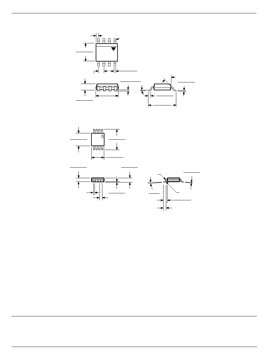
MIC284
Micrel
MIC284
20
September 29, 2000
Package Information
45
∞
0
∞≠8∞
0.244 (6.20)
0.228 (5.79)
0.197 (5.0)
0.189 (4.8)
SEATING
PLANE
0.026 (0.65)
MAX
)
0.010 (0.25)
0.007 (0.18)
0.064 (1.63)
0.045 (1.14)
0.0098 (0.249)
0.0040 (0.102)
0.020 (0.51)
0.013 (0.33)
0.157 (3.99)
0.150 (3.81)
0.050 (1.27)
TYP
PIN 1
DIMENSIONS:
INCHES (MM)
0.050 (1.27)
0.016 (0.40)
8-Lead SOP (M)
0.008 (0.20)
0.004 (0.10)
0.039 (0.99)
0.035 (0.89)
0.021 (0.53)
0.012 (0.03) R
0.0256 (0.65) TYP
0.012 (0.30) R
5
∞ MAX
0
∞ MIN
0.122 (3.10)
0.112 (2.84)
0.120 (3.05)
0.116 (2.95)
0.012 (0.03)
0.007 (0.18)
0.005 (0.13)
0.043 (1.09)
0.038 (0.97)
0.036 (0.90)
0.032 (0.81)
DIMENSIONS:
INCH (MM)
0.199 (5.05)
0.187 (4.74)
8-Lead MSOP (MM)
MICREL INC.
1849 FORTUNE DRIVE
SAN JOSE, CA 95131
USA
TEL
+ 1 (408) 944-0800
FAX
+ 1 (408) 944-0970
WEB
http://www.micrel.com
This information is believed to be accurate and reliable, however no responsibility is assumed by Micrel for its use nor for any infringement of patents or
other rights of third parties resulting from its use. No license is granted by implication or otherwise under any patent or patent right of Micrel Inc.
© 2000 Micrel Incorporated