July 1999
1
MIC29310/29312
MIC29310/29312
Micrel
General Description
The MIC29310 and MIC29312 are low cost versions of
MIC29300 family low-dropout (LDO) regulators. Manufac-
tured on Micrel's proprietary Super beta PNPTM process, the
MIC29310/2 is a 3A LDO regulator with very low-dropout
voltage (600mV over the full load) and low ground current.
Along with a total accuracy of
Ī
2% (over temperature, line
and load regulation) these regulators feature very fast tran-
sient recovery from input voltage surges and output load
current changes.
The MIC29310 is available in fixed 3.3V and 5V outputs
voltages; the MIC29312 has an adjustable output which can
be set by two external resistors to a voltage between 1.24V
to 15V. In addition, all versions are fully protected against
overcurrent faults, reversed input polarity, reversed lead
insertion, and overtemperature operation.
A TTL logic enable (EN) pin is available in the MIC29312 to
shutdown the regulator. When not used, the device can be
set to continuous operation by connecting EN to the input
(IN).
The MIC29310/2 is available in the standard 3- and 5-pin
TO-220 and TO-263 packages with an operating junction
temperature range of 0
į
C to +125
į
C.
Features
∑ Low cost versions of MIC29300 family
∑ Fast transient response
∑ 3A current over full temperature range
∑ 600mV dropout voltage at full load
∑ Low ground current
∑ Accurate 1% guaranteed tolerance
∑ "Zero" current shutdown mode (MIC29312)
∑ Fixed voltage and adjustable versions
Applications
∑ Processor peripheral and I/O supplies
∑ PC add-in cards
∑ High-efficiency "green" computer systems
∑ High-efficiency linear power supplies
∑ High-efficiency switching supply post regulator
∑ Battery-powered equipment
MIC29310/29312
3A Fast-Response LDO Regulator
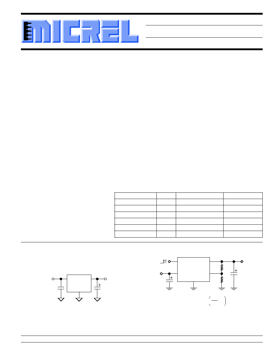
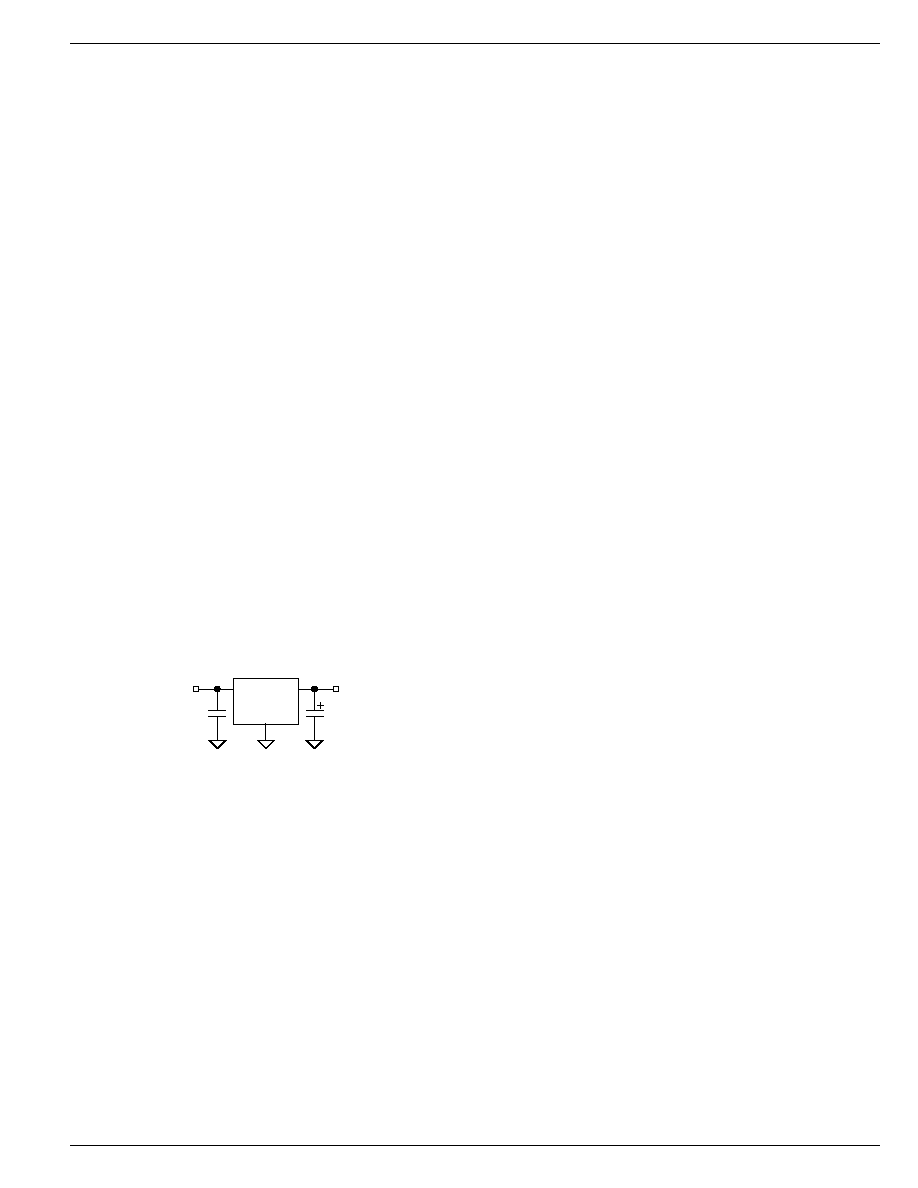
Typical Application
IN
OUT
GND
V
IN
V
OUT
Fixed Regulator Configuration
MIC29312
OUT
ADJ
R1*
V
OUT
* For best performance, total series resistance
(R1 + R2) should be small enough to pass
the minimum regulator load current of 10mA.
R2*
EN
GND
V
IN
IN
On
Off
V
OUT
= 1. 240
R1
R2
+ 1
Adjustable Regulator Configuration
Ordering Information
Part Number
Voltage
Junction Temp. Range
Package
MIC29310-3.3BT
3.3V
0
į
C to +125
į
C
TO-220-3
MIC29310-3.3BU
3.3V
0
į
C to +125
į
C
TO-263-3
MIC29310-5.0BT
5.0V
0
į
C to +125
į
C
TO-220-3
MIC29310-5.0BU
5.0V
0
į
C to +125
į
C
TO-263-3
MIC29312BT
Adj.
0
į
C to +125
į
C
TO-220-5
MIC29312BU
Adj.
0
į
C to +125
į
C
TO-263-5
For applications requiring even lower dropout
voltage, input voltage greater than 16V, or an
error flag, see the MIC29300/29301/29302/
29303.
Micrel, Inc. ∑ 1849 Fortune Drive ∑ San Jose, CA 95131 ∑ USA ∑ tel + 1 (408) 944-0800 ∑ fax + 1 (408) 944-0970 ∑ http://www.micrel.com

MIC29310/29312
Micrel
MIC29310/29312
2
July 1999
Pin Description
Pin Number
Pin Number
Pin Name
Pin Function
MIC29310
MIC29312
1
EN
Enable (Input): Active-high, logic-level enable/shutdown control.
1
2
IN
Unregulated Input: +16V maximum supply.
2,
TAB
3,
TAB
GND
Ground: Ground pin and
TAB
are internally connected.
3
4
OUT
Regulator Output
5
ADJ
Ouput Voltage Adjust: 1.24V feedback from external resistive divider.
Pin Configuration
TAB
3
OUT
2
GND
1
IN
MIC29310-x.xBT
TO-220 (T)
TAB
5
ADJ
4
OUT
3
GND
2
IN
1
EN
MIC29312-x.xBT
TO-220-5 (T)
TAB
3
OUT
2
GND
1
IN
MIC29310-x.xBU
TO-263 (U)
TAB
5
ADJ
4
OUT
3
GND
2
IN
1
EN
MIC29312-x.xBU
TO-263-5 (U)
Absolute Maximum Ratings
(Note 1)
Input Voltage (V
IN
) ........................................ ≠20V to +20V
Power Dissipation (P
D
) ............................ Internally Limited
Storage Temperature Range (T
S
) ............ ≠65
į
C to +150
į
C
Lead Temperature (soldering, 5 sec.) ....................... 260
į
C
ESD, Note 3
Operating Ratings
(Note 2)
Input Voltage (V
IN
) ....................................... +2.3V to +16V
Junction Temperature (T
J
) ........................... 0
į
C to +125
į
C
Package Thermal Resistance
TO-263
(
JC
) ......................................................... 2
į
C/W
TO-220 (
JC
) ......................................................... 2
į
C/W
TO-220 (
JA
) ....................................................... 55
į
C/W

July 1999
3
MIC29310/29312
MIC29310/29312
Micrel
Electrical Characteristics
T
J
= 25
į
C, bold values indicate 0
į
C
T
J
+125
į
C; unless noted
Parameter
Condition
Min
Typ
Max
Units
Output Voltage
10mA
I
O
I
FL
, (V
OUT
+ 1V)
V
IN
8V, Note 4
≠2
2
%
Line Regulation
I
O
= 10mA, (V
OUT
+ 1V)
V
IN
16V
0.06
0.5
%
Load Regulation
V
IN
= V
OUT
+ 1V, 10mA
I
OUT
I
FULL LOAD
, Notes 4, 8
0.2
1
%
V
O
/
T
Output Voltage Temperature Coefficient, Note 8
20
100
ppm/
į
C
Dropout Voltage
V
OUT
= ≠1%, Note 5
I
O
= 100mA
80
200
mV
I
O
= 750mA
220
mV
I
O
= 1.5A
330
mV
I
O
= 3A
600
1000
mV
Ground Current
I
O
= 750mA, V
IN
= V
OUT
+ 1V
5
20
mA
I
O
= 1.5A
15
mA
I
O
= 3A
60
150
mA
I
GNDDO
Ground Pin
V
IN
= 0.5V less than specified V
OUT
. I
OUT
= 10mA
2
3
mA
Current at Dropout
Current Limit
V
OUT
= 0V, Note 6
3.0
3.8
A
Minimum Load Current
7
10
mA
e
n
, Output Noise Voltage
C
L
= 10
Ķ
F
400
Ķ
V
RMS
(10Hz to 100kHz) I
L
= 100mA
C
L
= 33
Ķ
F
260
Ķ
V
RMS
Reference (MIC29312 only)
Reference Voltage
10mA
I
O
I
FL
, V
OUT
+ 1V
V
IN
8V, Note 4
1.215
1.265
V
MAX
Adjust Pin Bias Current
40
80
nA
120
nA
Reference Voltage
Note 9
20
ppm/
į
C
Temperature Coefficient
Adjust Pin Bias Current
0.1
nA/
į
C
Temperature Coefficient
Enable Input (MIC29312 only)
Input Logic Voltage
low (off)
0.8
V
high (on)
2.4
V
Enable Pin Input Current
V
EN
= V
IN
15
30
Ķ
A
75
Ķ
A
V
EN
= 0.8V
≠
2
Ķ
A
4
Ķ
A
Regulator Output
Note 10
10
Ķ
A
Current in Shutdown
20
Ķ
A
Note 1.
Exceeding the absolute maximum rating may damage the device.
Note 2.
The device is not guaranteed to function outside its operating rating.
Note 3.
Devices are ESD sensitive. Handling precautions recommended.
Note 4:
Full Load current is defined as 3A for the MIC29310/29312. For testing, V
OUT
is programmed to 5V.
Note 5:
Dropout voltage is defined as the input-to-output differential when the output voltage drops to 99% of its nominal value with V
OUT
+ 1V applied
to V
IN
.
Note 6:
For this test, V
IN
is the larger of 8V or V
OUT
+ 3V.
Note 7:
Ground pin current is the regulator quiescent current. The total current drawn from the source is the sum of the load current plus the ground
pin current.
Note 8:
Output voltage temperature coefficient is defined as the worst case voltage change divided by the total temperature range.
Note 9:
V
REF
V
OUT
(V
IN
≠ 1V), 2.4V
V
IN
16V, 10mA < I
L
I
FL
, T
J
T
J(max).
Note 10: V
EN
0.8V and V
IN
8V, V
OUT
= 0.
MIC29310/29312
Micrel
MIC29310/29312
4
July 1999
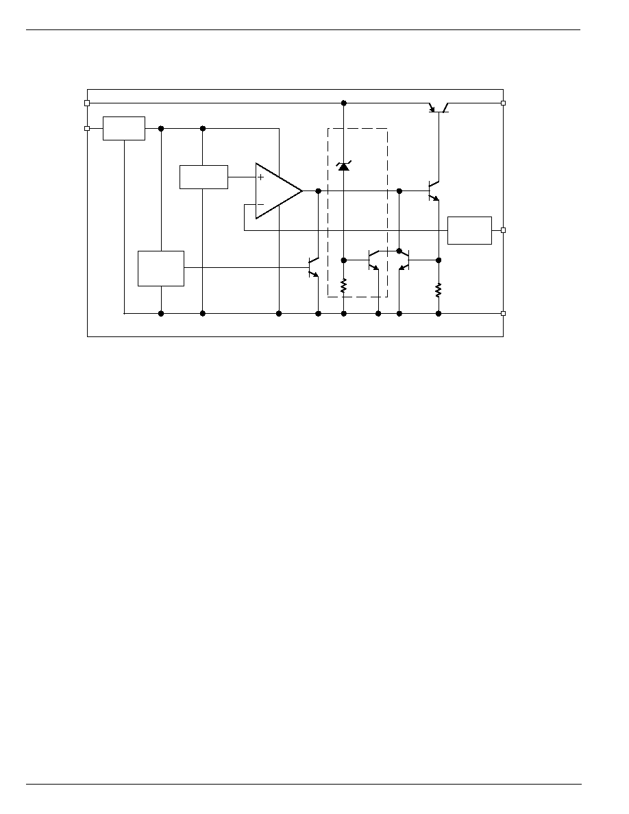
Block Diagram
On/Off
Reference
Bias
Feed-
back
GND
16V
OUT
ADJ*
*EN
IN
O.V.
I
LIMIT
Thermal
Shut-
down
* MIC29312 only.
MIC29310/29312
July 1999
5
MIC29310/29312
MIC29310/29312
Micrel
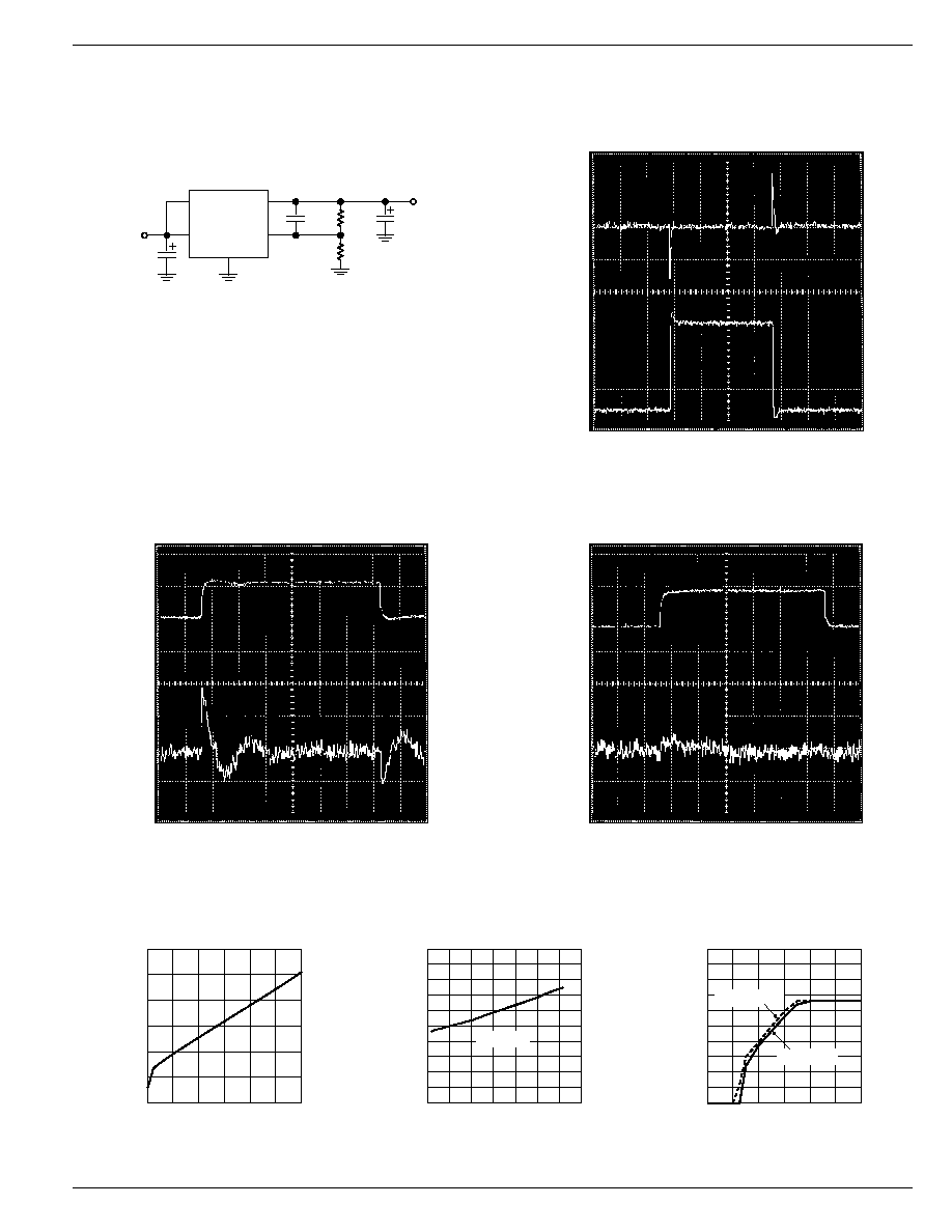
0.00
0.10
0.20
0.30
0.40
0.50
0.60
0
1
2
3
DROPOUT VOLTAGE (V)
OUTPUT CURRENT (A)
MIC2931x Dropout Voltage
vs. Output Current
0
0.2
0.4
0.6
0.8
1
-60 -30
0
30
60
90 120 150
DROPOUT VOLTAGE (mV)
TEMPERATURE (
į
C)
MIC2931x Dropout Voltage
vs. Temperature
I
LOAD
= 3A
0.0
1.0
2.0
3.0
4.0
5.0
0
2
4
6
OUTPUT VOLTAGE (V)
INPUT VOLTAGE (V)
MIC29310-3.3
Dropout Characteristics
I
LOAD
= 3A
I
LOAD
= 10mA
Typical Characteristics
0mA
200mA
3A
3.525V
+20mV
≠20mV
LOAD CURRENT OUTPUT VOLTAGE
MIC29312 Load Transient Response
(See Test Circuit Schematic)
1ms/division
6.525V
4.525V
3.525V
+20mV
≠20mV
OUTPUT VOLTAGE INPUT VOLTAGE
MIC29312 Line Transient Response
with 3A Load, 10
Ķ
F Output Capacitance
200
Ķ
s/division
I
OUT
= 3A
C
OUT
=10
Ķ
F
6.525V
4.525V
3.525V
+20mV
≠20mV
OUTPUT VOLTAGE INPUT VOLTAGE
MIC29312 Line Transient Response
with 3A Load, 100
Ķ
F Output Capacitance
200
Ķ
s/division
I
OUT
= 3A
C
OUT
= 100
Ķ
F
V
IN
= V
OUT
+ 1V
MIC29312
EN
IN
OUT
ADJ
GND
0.1ĶF
93.1k
1%
49.9k
1%
V
OUT
3.525V nominal
4
◊
330ĶF
AVX
TPSE337M006R0100
tantalum
V
OUT
load (not shown):
Intelģ Power Validator
MIC29312 Load Transient Response Test Circuit
MIC29310/29312
Micrel
MIC29310/29312
6
July 1999
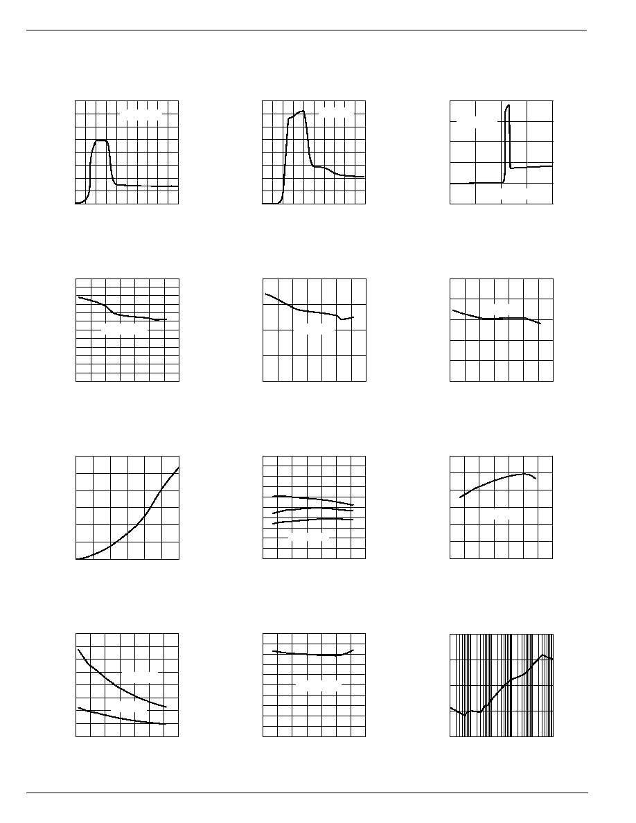
0
10
20
30
40
50
-60 -30
0
30
60
90 120 150
ADJUST PIN CURRENT (nA)
TEMPERATURE (
į
C)
MIC29312 Adjust Pin Current
vs. Temperature
I
LOAD
= 10mA
0.0
1.0
2.0
3.0
4.0
5.0
6.0
-60 -30
0
30
60
90 120 150
GROUND CURRENT (mA)
TEMPERATURE (
į
C)
MIC2931x Ground Current
vs. Temperature
I
OUT
= 750mA
0
5
10
15
20
-60 -30
0
30
60
90 120 150
GROUND CURRENT (mA)
TEMPERATURE (
į
C)
MIC2931x Ground Current
vs. Temperature
I
OUT
= 1.5A
0
20
40
60
80
100
-60 -30
0
30
60
90 120 150
GROUND CURRENT (mA)
TEMPERATURE (
į
C)
MIC2931x Ground Current
vs. Temperature
I
OUT
= 3A
0
10
20
30
40
50
60
0
1
2
3
GROUND CURRENT (mA)
OUTPUT CURRENT (A)
MIC2931x Ground Current
vs. Output Current
3.20
3.22
3.24
3.26
3.28
3.30
3.32
3.34
3.36
3.38
3.40
-60 -30
0
30
60
90 120 150
OUTPUT VOLTAGE (V)
TEMPERATURE (
į
C)
MIC29310-3.3 Output Voltage
vs. Temperature
3 DEVICES
0
1
2
3
4
5
6
-60 -30
0
30
60
90 120 150
CURRENT (A)
TEMPERATURE (
į
C)
MIC2931x Short Circuit
Current vs. Temperature
V
OUT
= 0V
0
5
10
15
20
25
30
35
40
-60 -30
0
30
60
90 120 150
ENABLE CURRENT (
Ķ
A)
TEMPERATURE (
į
C)
MIC29312 Enable Current
vs. Temperaure
V
EN
= 5V
V
EN
= 2V
0.001
0.01
0.1
1
10
10x10
0
100x10
0
1x10
3
10x10
3
100x10
3
1x10
6
OUTPUT IMPEDANCE (
)
FREQUENCY (Hz)
MIC2931x Output Impedance
vs. Frequency
0.0
0.5
1.0
1.5
2.0
0
2
4
6
8
10
GROUND CURRENT (mA)
INPUT VOLTAGE (V)
MIC2931x Ground Current
vs. Input Voltage
I
OUT
= 10mA
0
50
100
150
200
0
2
4
6
8
10
GROUND CURRENT (mA)
INPUT VOLTAGE (V)
MIC2931x Ground Current
vs. Input Voltage
I
OUT
= 3A
-0.5
0.0
0.5
1.0
1.5
2.0
-20
-10
0
10
20
GROUND CURRENT (mA)
INPUT VOLTAGE (V)
MIC2931x Ground Current
vs. Input Voltage
R
LOAD
= 100
V
OUT
= 3.3V
July 1999
7
MIC29310/29312
MIC29310/29312
Micrel
Applications Information
The MIC29310 and MIC29312 are high performance low-
dropout voltage regulators suitable for all moderate to high-
current voltage regulator applications. Their 600mV of drop-
out voltage at full load make them especially valuable in
battery powered systems and as high efficiency noise filters
in "post-regulator" applications. Unlike older NPN-pass tran-
sistor designs, where the minimum dropout voltage is limited
by the base-emitter voltage drop and collector-emitter satu-
ration voltage, dropout performance of the PNP output of
these devices is limited merely by the low V
CE
saturation
voltage.
A trade-off for the low dropout voltage is a varying base drive
requirement. But Micrel's Super Ŗeta PNPTM process re-
duces this drive requirement to merely 2% to 5% of the load
current.
MIC29310/312 regulators are fully protected from damage
due to fault conditions. Current limiting is provided. This
limiting is linear; output current under overload conditions is
constant. Thermal shutdown disables the device when the
die temperature exceeds the maximum safe operating tem-
perature. Transient protection allows device (and load) sur-
vival even when the input voltage spike above and below
nominal. The output structure of these regulators allows
voltages in excess of the desired output voltage to be applied
without reverse current flow. The MIC29312 version offers a
logic level ON/OFF control: when disabled, the devices draw
nearly zero current.
An additional feature of this regulator family is a common
pinout: a design's current requirement may change up or
down yet use the same board layout, as all of Micrel's high-
current Super Ŗeta PNPTM regulators have identical pinouts.
IN
OUT
GND
V
IN
V
OUT
Figure 3. The MIC29310 regulator requires only two
capacitors for operation.
Thermal Design
Linear regulators are simple to use. The most complicated
design parameters to consider are thermal characteristics.
Thermal design requires the following application-specific
parameters:
∑ Maximum ambient temperature, T
A
∑ Output Current, I
OUT
∑ Output Voltage, V
OUT
∑ Input Voltage, V
IN
First, we calculate the power dissipation of the regulator from
these numbers and the device parameters from this datasheet.
P
D
= I
OUT
◊
(1.02V
IN
≠ V
OUT
)
Where the ground current is approximated by 2% of I
OUT
.
Then the heat sink thermal resistance is determined with this
formula:
T
J MAX
≠ T
A
SA
= ------------ ≠ (
JC
+
CS
)
P
D
Where T
J MAX
125
į
C and
CS
is between 0 and 2
į
C/W.
The heat sink may be significantly reduced in applications
where the minimum input voltage is known and is large
compared with the dropout voltage. Use a series input
resistor to drop excessive voltage and distribute the heat
between this resistor and the regulator. The low dropout
properties of Micrel Super Ŗeta PNP regulators allow very
significant reductions in regulator power dissipation and the
associated heat sink without compromising performance.
When this technique is employed, a capacitor of at least
0.1
Ķ
F is needed directly between the input and regulator
ground.
Please refer to Application Note 9 for further details and
examples on thermal design and heat sink specification.
Capacitor Requirements
For stability and minimum output noise, a capacitor on the
regulator output is necessary. The value of this capacitor is
dependent upon the output current; lower currents allow
smaller capacitors. MIC29310/2 regulators are stable with a
minimum capacitor value of 10
Ķ
F at full load.
This capacitor need not be an expensive low ESR type:
aluminum electrolytics are adequate. In fact, extremely low
ESR capacitors may contribute to instability. Tantalum ca-
pacitors are recommended for systems where fast load
transient response is important.
Where the regulator is powered from a source with a high AC
impedance, a 0.1
Ķ
F capacitor connected between Input and
GND is recommended. This capacitor should have good
characteristics to above 250kHz.
Transient Response and 5V to 3.3V Conversion
The MIC29310/2 have excellent response to variations in
input voltage and load current. By virtue of their low dropout
voltage, these devices do not saturate into dropout as readily
as similar NPN-based designs. A 3.3V output Micrel LDO will
maintain full speed and performance with an input supply as
low as 4.2V, and will still provide some regulation with
supplies down to 3.8V, unlike NPN devices that require 5.1V
or more for good performance and become nothing more
than a resistor under 4.6V of input. Micrel's PNP regulators
provide superior performance in "5V to 3.3V" conversion
applications than NPN regulators, especially when all toler-
ances are considered.
Minimum Load Current
The MIC29310/2 regulators are specified between finite
MIC29310/29312
Micrel
MIC29310/29312
8
July 1999
loads. If the output current is too small, leakage currents
dominate and the output voltage rises. A 10mA minimum
load current is necessary for proper regulation.
Adjustable Regulator Design
R1
100k
R2
56.2k
VOUT = 1.240V
◊
[1 + (R1 / R2)]
VIN
4.75V to 5.25V
VOUT
3.45V
MIC29312BT
22ĶF
10ĶF
Figure 4. Adjustable Regulator with Resistors
The adjustable regulator version, MIC29312, allows pro-
gramming the output voltage anywhere between 1.25V and
the 15V maximum operating rating of the family. Two resis-
tors are used. Resistors can be quite large, up to 1M
,
because of the very high input impedance and low bias
current of the sense comparator. The resistor values are
calculated by:
V
OUT
R1 = R2
◊
( ≠---- ≠ 1 )
1.240
Where V
O
is the desired output voltage. Figure 4 shows
component definition. Applications with widely varying load
currents may scale the resistors to draw the minimum load
current required for proper operation (see the table below).
Enable Input
The MIC29312 version features an enable (EN) input that
allows ON/OFF control of the device. Special design allows
"zero" current drain when the device is disabled--only micro-
amperes of leakage current flows. The EN input has TTL/
CMOS compatible thresholds for simple interfacing with
logic, or may be directly tied to V
IN
. Enabling the regulator
requires approximately 20
Ķ
A of current into the EN pin.
Resistor Value Table for the MIC29312 Adjustable Regulator
Note: This regulator has a minimum load requirement. "Standard" values assume the load meets this requirement. "Minimum
Load" values are calculated to draw 10mA and allow regulation with an open load (the minimum current drawn from the load
may be zero).
Voltage
Standard (
)
Min. Load (
)
R1
R2
R1
R2
2.85
100k
76.8k
162
124
2.9
100k
75.0k
165
124
3.0
100k
69.8k
174
124
3.1
100k
66.5k
187
124
3.15
100k
64.9k
191
124
3.3
100k
60.4k
205
124
3.45
100k
56.2k
221
124
3.6
100k
52.3k
237
124
3.8
100k
48.7k
255
124
4.0
100k
45.3k
274
124
4.1
100k
43.2k
287
124
July 1999
9
MIC29310/29312
MIC29310/29312
Micrel
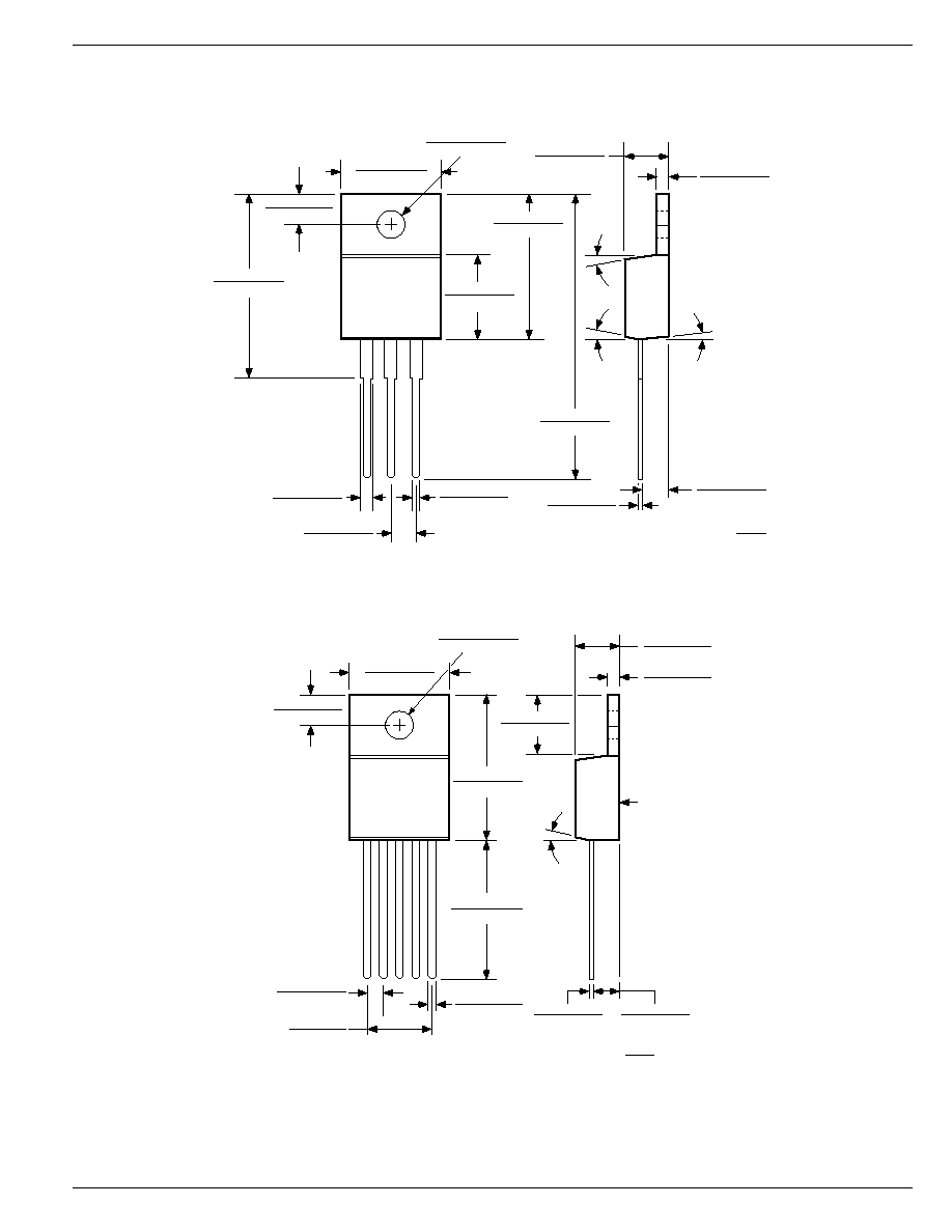
Package Information
0.018
Ī
0.008
(0.46
Ī
0.020)
0.100
Ī
0.005
(2.54
Ī
0.13)
0.030
Ī
0.003
(0.76
Ī
0.08)
0.050
Ī
0.003
(1.27
Ī
.08)
7
į
1.140
Ī
0.010
(28.96
Ī
0.25)
0.356
Ī
0.005
(9.04
Ī
0.13)
0.590
Ī
0.005
(14.99
Ī
0.13)
0.108
Ī
0.005
(2.74
Ī
0.13)
0.050
Ī
0.005
(1.27
Ī
0.13)
0.151 D
Ī
0.005
(3.84 D
Ī
0.13)
0.410
Ī
0.010
(10.41
Ī
0.25)
0.176
Ī
0.005
(4.47
Ī
0.13)
0.100
Ī
0.020
(2.54
Ī
0.51)
0.818
Ī
0.005
(20.78
Ī
0.13)
7
į
3
į
DIMENSIONS: INCH
(MM)
TO-220-3 (T)
0.018
Ī
0.008
(0.46
Ī
0.20)
0.268 REF
(6.81 REF)
0.032
Ī
0.005
(0.81
Ī
0.13)
0.550
Ī
0.010
(13.97
Ī
0.25)
7
į
Typ.
SEATING
PLANE
0.578
Ī
0.018
(14.68
Ī
0.46)
0.108
Ī
0.005
(2.74
Ī
0.13)
0.050
Ī
0.005
(1.27
Ī
0.13)
0.150 D
Ī
0.005
(3.81 D
Ī
0.13)
0.400
Ī
0.015
(10.16
Ī
0.38)
0.177
Ī
0.008
(4.50
Ī
0.20)
0.103
Ī
0.013
(2.62
Ī
0.33)
0.241
Ī
0.017
(6.12
Ī
0.43)
0.067
Ī
0.005
(1.70
Ī
0.127)
inch
(mm)
Dimensions:
TO-220-5 (T)
MIC29310/29312
Micrel
MIC29310/29312
10
July 1999
0.360
Ī
0.005
0.600
Ī
0.025
0.405
Ī
0.005
0.100 BSC
0.050
0.050
Ī
0.005
0.176
Ī
0.005
8
į
MAX
0.100
Ī
0.01
0.050
Ī
0.005
0.015
Ī
0.002
0.004+0.004
≠0.008
SEATING PLANE
0.065
Ī
0.010
20
įĪ
2
į
DIM. = INCH
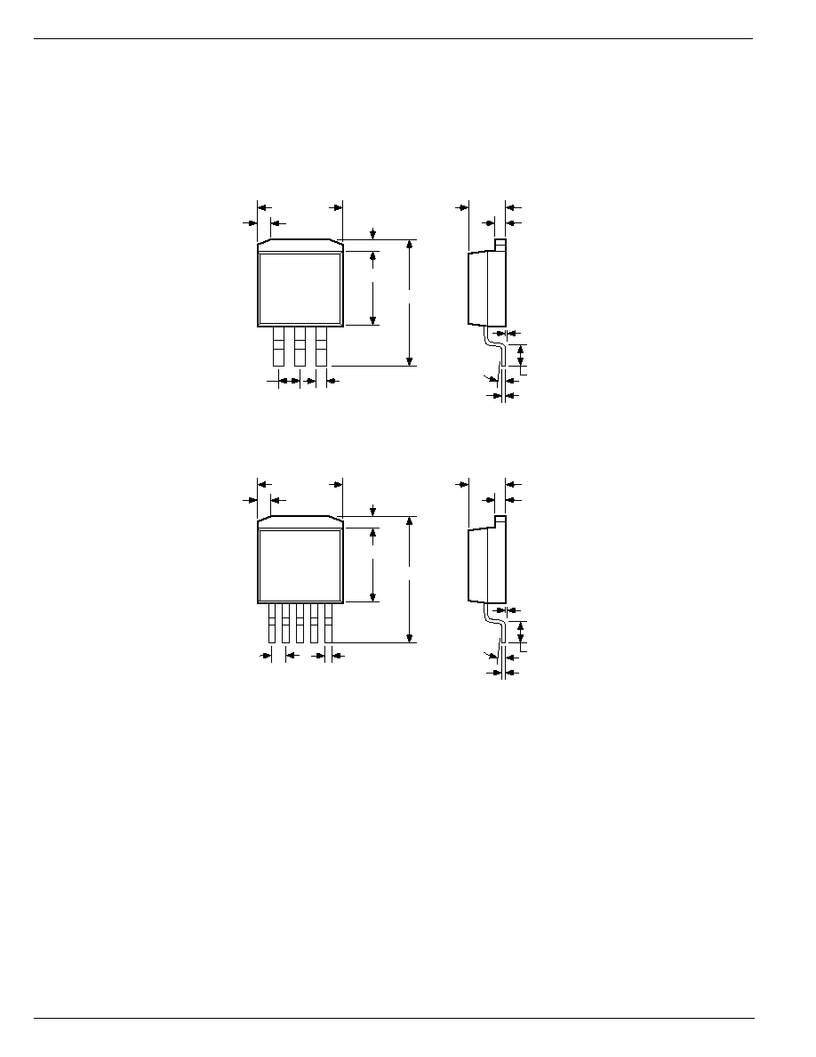
TO-263-3 (U)
0.067
Ī
0.005
0.032
Ī
0.003
0.360
Ī
0.005
0.600
Ī
0.025
0.405
Ī
0.005
0.060
Ī
0.005
0.176
Ī
0.005
8
į
MAX
0.100
Ī
0.01
0.050
Ī
0.005
0.015
Ī
0.002
0.004+0.004
≠0.008
SEATING PLANE
0.065
Ī
0.010
20
įĪ
2
į
DIM. = INCH
TO-263-5 (U)

July 1999
11
MIC29310/29312
MIC29310/29312
Micrel

MIC29310/29312
Micrel
MIC29310/29312
12
July 1999
MICREL INC.
1849 FORTUNE DRIVE
SAN JOSE, CA 95131
USA
TEL
+ 1 (408) 944-0800
FAX
+ 1 (408) 944-0970
WEB
http://www.micrel.com
This information is believed to be accurate and reliable, however no responsibility is assumed by Micrel for its use nor for any infringement of patents or
other rights of third parties resulting from its use. No license is granted by implication or otherwise under any patent or patent right of Micrel Inc.
© 1999 Micrel Incorporated