MIC2937A/29371/29372
Micrel
3-18
October 1999
1
2
3
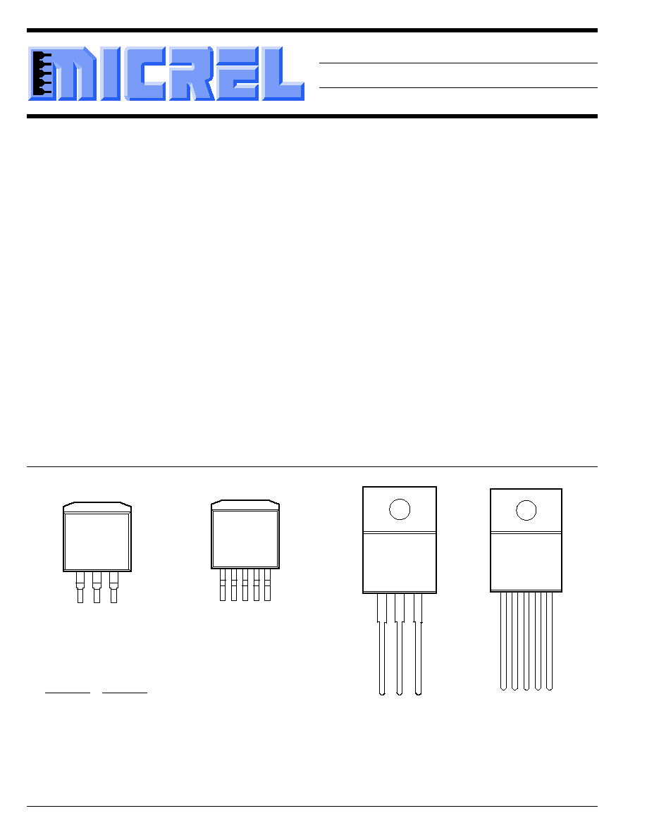
Front View
Features
∑
High output voltage accuracy
∑
Guaranteed 750mA output
∑
Low quiescent current
∑
Low dropout voltage
∑
Extremely tight load and line regulation
∑
Very low temperature coefficient
∑
Current and thermal limiting
∑
Input can withstand ≠20V reverse battery and +60V
positive transients
∑
Error flag warns of output dropout
∑
Logic-controlled electronic shutdown
∑
Output programmable from 1.24V to 26V(MIC29372)
∑
Available in TO-220, TO-263, TO-220-5, and TO-263-5
packages.
Applications
∑
Battery Powered Equipment
∑
Cellular Telephones
∑
Laptop, Notebook, and Palmtop Computers
∑
PCMCIA V
CC
and V
PP
Regulation/Switching
∑
Bar Code Scanners
∑
Automotive Electronics
∑
SMPS Post-Regulator/ DC to DC Modules
∑
High Efficiency Linear Power Supplies
Pin Configuration
GROUND OUTPUT
INPUT
TO-220-5 Package
(MIC29371/29372BT)
TO-220 Package
(MIC2937A-xxBT)
1
2 3 4 5
General Description
The MIC2937A family are "bulletproof" efficient voltage
regulators with very low dropout voltage (typically 40mV at
light loads and 300mV at 500mA), and very low quiescent
current (160
µ
A typical). The quiescent current of the MIC2937A
increases only slightly in dropout, thus prolonging battery life.
Key MIC2937A features include protection against reversed
battery, fold-back current limiting, and automotive "load dump"
protection (60V positive transient).
The MIC2937 is available in several configurations. The
MIC2937A-xx devices are three pin fixed voltage regulators
with 3.3V, 5V, and 12V outputs available. The MIC29371 is a
fixed regulator offering logic compatible ON/OFF switching
input and an error flag output. This flag may also be used as
a power-on reset signal. A logic-compatible shutdown input is
provided on the adjustable MIC29372, which enables the
regulator to be switched on and off.
TO-263 Package
(MIC2937A-xxBU)
GROUND OUTPUT
INPUT
TO-263-5 Package
(MIC29371/29372BU)
1
2 3 4 5
Five Lead Package Pin Functions:
MIC29371
MIC29372
1)
Error
Adjust
2)
Input
Shutdown
3)
Ground
Ground
4)
Output
Input
5)
Shutdown
Output
The TAB is Ground on the TO-220 and TO-263 packages.
MIC2937A/29371/29372
750mA Low-Dropout Voltage Regulator
MIC2937A/29371/29372
Micrel
October 1999
19
MIC2937A/29371/29372
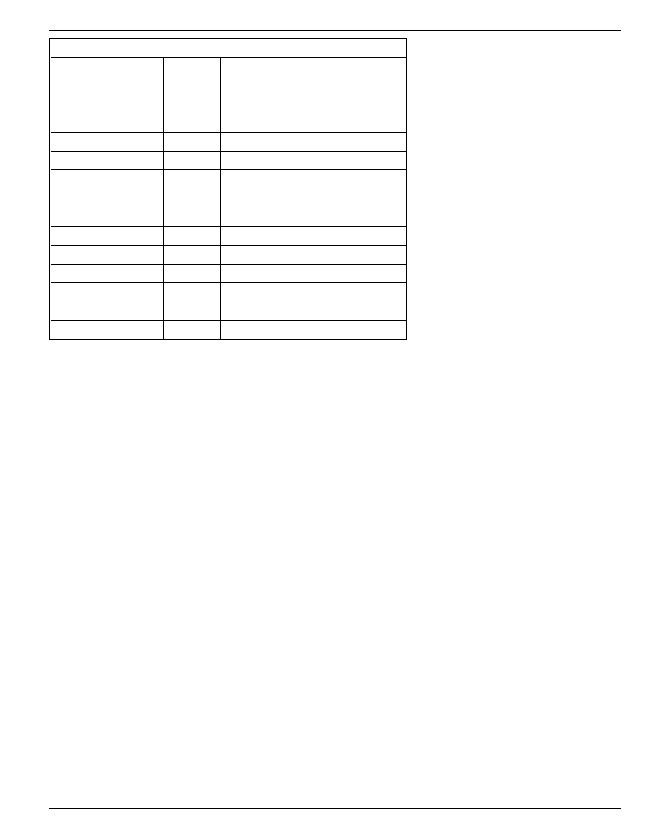
Ordering Information
Part Number
Voltage
Temperature Range*
Package
MIC2937A-3.3BU
3.3
≠40
∞
C to +125
∞
C
TO-263-3
MIC2937A-3.3BT
3.3
≠40
∞
C to +125
∞
C
TO-220
MIC2937A-5.0BU
5.0
≠40
∞
C to +125
∞
C
TO-263-3
MIC2937A-5.0BT
5.0
≠40
∞
C to +125
∞
C
TO-220
MIC2937A-12BU
12
≠40
∞
C to +125
∞
C
TO-263-3
MIC2937A-12BT
12
≠40
∞
C to +125
∞
C
TO-220
MIC29371-3.3BT
3.3
≠40
∞
C to +125
∞
C
TO-220-5
MIC29371-3.3BU
3.3
≠40
∞
C to +125
∞
C
TO-263-5
MIC29371-5.0BT
5.0
≠40
∞
C to +125
∞
C
TO-220-5
MIC29371-5.0BU
5.0
≠40
∞
C to +125
∞
C
TO-263-5
MIC29371-12BT
12
≠40
∞
C to +125
∞
C
TO-220-5
MIC29371-12BU
12
≠40
∞
C to +125
∞
C
TO-263-5
MIC29372BT
Adj
≠40
∞
C to +125
∞
C
TO-220-5
MIC29372BU
Adj
≠40
∞
C to +125
∞
C
TO-263-5
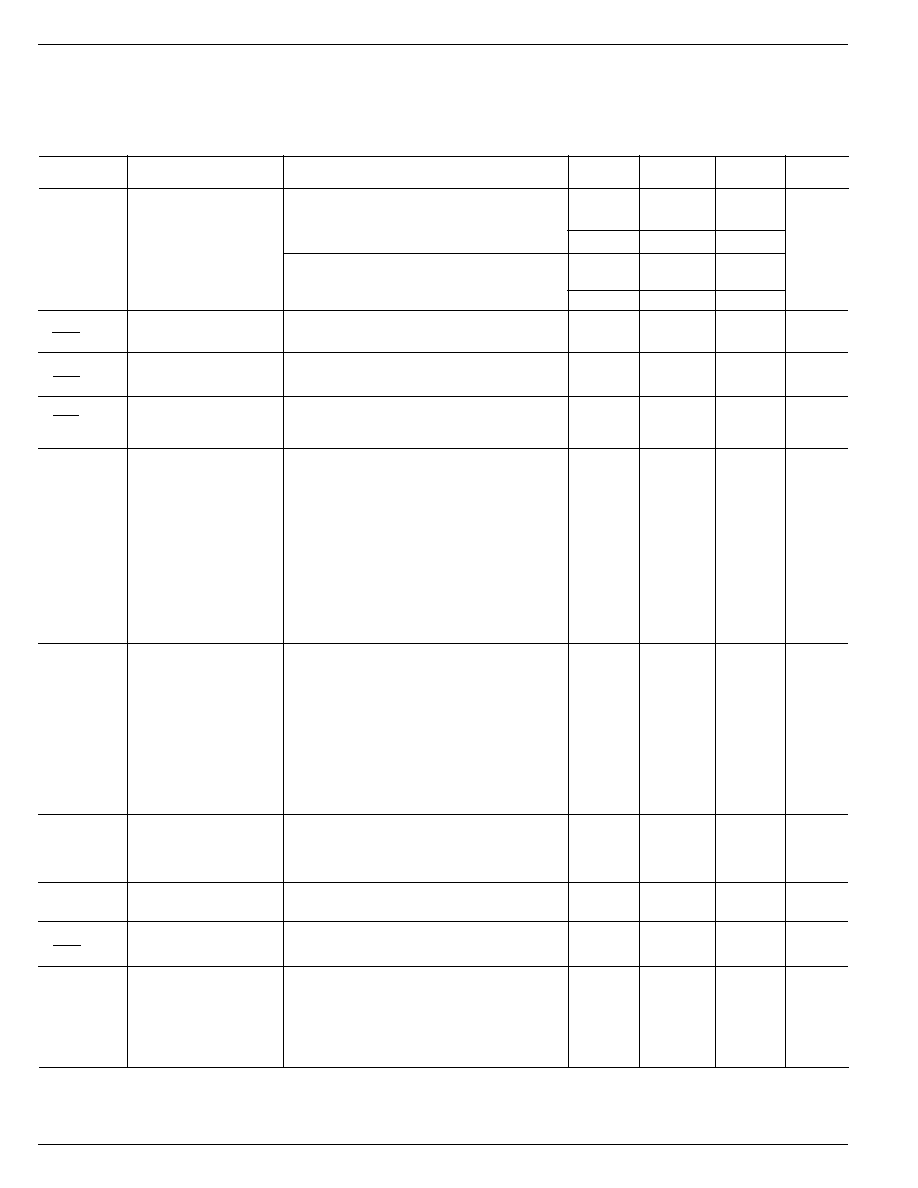
Absolute Maximum Ratings
If Military/Aerospace specified devices
are required, contact your local Micrel
representative/distributor for availability
and specifications.
Power Dissipation (Note 1) .............. Internally Limited
Lead Temperature (Soldering, 5 seconds) ........ 260
∞
C
Storage Temperature Range ............ ≠65
∞
C to +150
∞
C
Operating Junction Temperature Range
................................................. ≠40
∞
C to +125
∞
C
TO-220
JC
...................................................... 2.5
∞
C/W
TO-263
JC
...................................................... 2.5
∞
C/W
Input Supply Voltage ............................... ≠20V to +60V
Operating Input Supply Voltage ................... 2V
to 26V
Adjust Input Voltage (Notes 9 and 10)
...................................................... ≠1.5V to +26V
Shutdown Input Voltage ......................... ≠0.3V to +30V
Error Comparator Output Voltage .......... ≠0.3V to +30V
Across the full operating temperature, the minimum
input voltage range for full output current is 4.3V to 26V.
Output will remain in-regulation at lower output voltages
and low current loads down to an input of 2V at 25
∞
C.
*
Junction temperatures
MIC2937A/29371/29372
Micrel
MIC2937A/29371/29372
20
October 1999
Electrical Characteristics
Limits in standard typeface are for T
J
= 25
∞
C and limits in boldface apply over the full operating temperature range.
Unless otherwise specified, V
IN
= V
OUT
+ 1V, I
L
= 5mA, C
L
= 10
µ
F. The MIC29372 are programmed for a 5V output voltage,
and V
SHUTDOWN
0.6V (MIC29371-xx and MIC29372 only).
Symbol
Parameter
Conditions
Min
Typical
Max
Units
V
O
Output Voltage
Variation from factory trimmed V
OUT
≠1
1
%
Accuracy
≠2
2
5mA
I
L
500mA
≠2.5
2.5
MIC2937A-12 and 29371-12 only:
≠1.5
1.5
≠3
3
5mA
I
L
500mA
≠4
4
V
O
Output Voltage
(Note 2)
20
100
ppm/
∞
C
T
Temperature Coef.
Output voltage > 10V
80
350
V
O
Line Regulation
V
IN
= V
OUT
+ 1V to 26V
0.03
0.10
%
V
O
0.40
V
O
Load Regulation
I
L
= 5 to 500mA
0.04
0.16
%
V
O
(Note 3)
0.30
V
IN
≠ V
O
Dropout Voltage
I
L
= 5mA
80
150
mV
(Note 4)
180
I
L
= 100mA
200
Output voltage > 10V
240
I
L
= 500mA
300
Output voltage > 10V
420
I
L
= 750mA
370
600
750
I
GND
Ground Pin Current
I
L
= 5mA
160
250
µ
A
(Note 5)
300
I
L
= 100mA
1
2.5
mA
3
I
L
= 500mA
8
13
16
I
L
= 750mA
15
25
I
GNDDO
Ground Pin
V
IN
= 0.5V less than designed V
OUT
200
500
µ
A
Current at Dropout
(V
OUT
3.3V)
(Note 5)
I
O
= 5mA
I
LIMIT
Current Limit
V
OUT
= 0V
1.1
1.5
A
(Note 6)
2
V
O
Thermal Regulation
(Note 7)
0.05
0.2
%/W
P
D
e
n
Output Noise
C
L
= 10
µ
F
400
µ
V RMS
Voltage
(10Hz to 100kHz)
C
L
= 100
µ
F
260
I
L
= 100mA
MIC2937A/29371/29372
Micrel
October 1999
21
MIC2937A/29371/29372
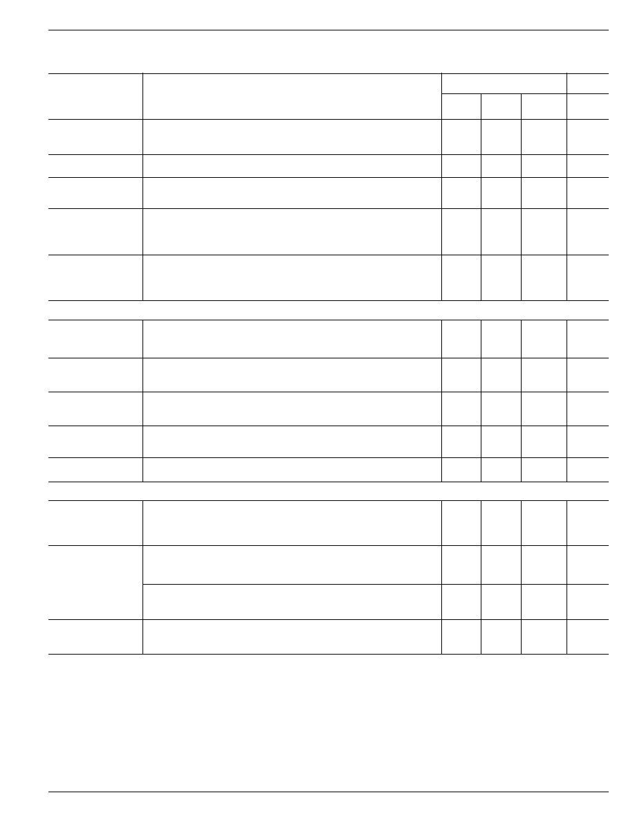
Electrical Characteristics
(Continued)
Parameter
Conditions
Min
Typical
Max
Units
Reference Voltage
1.223
1.235
1.247
V
1.210
1.260
V max
Reference Voltage
(Note 8)
1.204
1.266
V
Adjust Pin
20
40
nA
Bias Current
60
Reference Voltage
(Note 7)
20
ppm/
∞
C
Temperature
Coefficient
Adjust Pin Bias
0.1
nA/
∞
C
Current Temperature
Coefficient
Error Comparator
Output Leakage
V
OH
= 26V
0.01
1.00
µ
A
Current
2.00
Output Low
V
IN
= 4.5V
150
250
mV
Voltage
I
OL
= 250
µ
A
400
Upper Threshold
(Note 9)
40
60
mV
Voltage
25
Lower Threshold
(Note 9)
75
95
mV
Voltage
140
Hysteresis
(Note 9)
15
mV
Shutdown Input
Input Logic Voltage
1.3
V
Low (ON)
0.7
High (OFF)
2.0
Shutdown Pin
V
SHUTDOWN
= 2.4V
30
50
µ
A
Input Current
100
V
SHUTDOWN
= 26V
450
600
µ
A
750
Regulator Output
(Note 10)
3
10
µ
A
Current in Shutdown
20
MIC29371
MIC29371/MIC29372
MIC29372
MIC2937A/29371/29372
Micrel
MIC2937A/29371/29372
22
October 1999
Note 1:
Absolute maximum ratings indicate limits beyond which damage to the component may occur. Electrical specifications do not
apply when operating the device outside of its rated operating conditions. The maximum allowable power dissipation is a function of the
maximum junction temperature, T
J (MAX)
, the junction-to-ambient thermal resistance,
JA
, and the ambient temperature, T
A
. The maximum
allowable power dissipation at any ambient temperature is calculated using: P
(MAX)
= (T
J(MAX)
≠ T
A
)
/
JA.
Exceeding the maximum allowable
power dissipation will result in excessive die temperature, and the regulator will go into thermal shutdown.
Note 2:
Output voltage temperature coefficient is defined as the worst case voltage change divided by the total temperature range.
Note 3:
Regulation is measured at constant junction temperature using low duty cycle pulse testing. Changes in output voltage due to
heating effects are covered by the thermal regulation specification.
Note 4:
Dropout Voltage is defined as the input to output differential at which the output voltage drops 100 mV below its nominal value
measured at 1V differential. At low values of programmed output voltage, the minimum input supply voltage of 4.3V over temperature must
be taken into account. The MIC2937A operates down to 2V of input at reduced output current at 25
∞
C.
Note 5:
Ground pin current is the regulator quiescent current. The total current drawn from the source is the sum of the load current plus
the ground pin current.
Note 6:
The MIC2937A family features fold-back current limiting. The short circuit (V
OUT
= 0V) current limit is less than the maximum current
with normal output voltage.
Note 7:
Thermal regulation is defined as the change in output voltage at a time T after a change in power dissipation is applied, excluding
load or line regulation effects. Specifications are for a 200mA load pulse at V
IN
= 20V (a 4W pulse) for T = 10ms.
Note 8:
V
REF
V
OUT
(V
IN
≠ 1 V), 4.3V
V
IN
26V, 5mA < I
L
750 mA, T
J
T
J MAX.
Note 9:
Comparator thresholds are expressed in terms of a voltage differential at the Adjust terminal below the nominal reference voltage
measured at 6V input (for a 5V regulator). To express these thresholds in terms of output voltage change, multiply by the error amplifier gain
= V
OUT
/V
REF
= (R1 + R2)/R2. For example, at a programmed output voltage of 5V, the Error output is guaranteed to go low when the output
drops by 95 mV x 5V/1.235 V = 384 mV. Thresholds remain constant as a percent of V
OUT
as V
OUT
is varied, with the dropout warning
occurring at typically 5% below nominal, 7.7% guaranteed.
Note 10: Circuit of Figure 3 with R1
150k
. V
SHUTDOWN
2V and V
IN
26V,V
OUT
= 0.
Note 11: When used in dual supply systems where the regulator load is returned to a negative supply, the output voltage must be diode
clamped to ground.
Note 12: Maximum positive supply voltage of 60V must be of limited duration (< 100ms) and duty cycle (
1%). The maximum continuous
supply voltage is 26V.
FEEDBACK
SENSE
Q15A
OUT
Q24
Q26
R27
V TAP
R28
R18
20k
Q25
Q23
Q22
R15
100 k
R16
30 k
Q29
Q28
R17
10
R21 8
R17
12 k
Q31
Q30
R23 60 k
SHDN
R24
50 k
R22
150 k
Q21
Q19
C2
40 pF
R14
350
k
Q14
R13
100
k
Q18
R12
110
k
Q20
Q9
Q15B
Q8
Q7
R11
20.6
k
Q5
R8
31.4 k
R10
150
k
R9
27.8 k
Q11
Q12
Q13
R6
140
k
R5
180
k
R4
13 k
R3
50 k
Q2
C1
20
pF
Q4
Q3
R11
18
k
Q6
Q1
10
R1
20 k
R2
50 k
Q41
R30
30
k
Q40
Q34
GND
Q36
Q37
R25
2.8 k
Q38
ERROR
R26
60 k
Q39
Q42
Q16
Q17
50 k
10 k
IN
DENOTES CONNECTION ON
MIC2937A-xx AND MIC29371-xx
VERSIONS ONLY
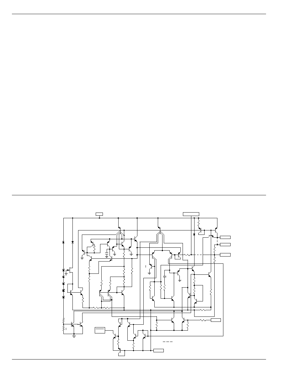
Schematic Diagram

MIC2937A/29371/29372
Micrel
October 1999
23
MIC2937A/29371/29372
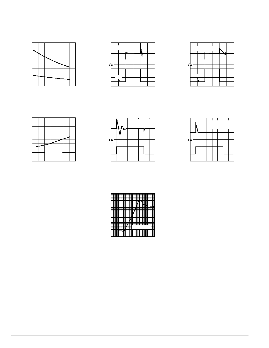
Typical Characteristics
0
100
200
300
400
500
0
200
400
600
800
DROPOUT VOLTAGE (mV)
OUTPUT CURRENT (mA)
Dropout Voltage
vs. Output Current
0
100
200
300
400
500
600
700
-60 -30
0
30
60
90 120 150
DROPOUT VOLTAGE (mV)
TEMPERATURE (
∞
C)
Dropout Voltage
vs. Temperature
I
LOAD
= 750mA
0
1
2
3
4
5
6
0
1
2
3
4
5
6
OUTPUT VOLTAGE (V)
INPUT VOLTAGE (V)
Dropout
Characteristics
I
LOAD
= 5mA
I
LOAD
= 750mA
0.1
1
10
30
1
10
100
1000
GROUND CURRENT (mA)
OUTPUT CURRENT (mA)
Ground Current
vs. Output Current
0
50
100
150
200
0
1
2
3
4
5
6
7
8
GROUND CURRENT (
µ
A)
SUPPLY VOLTAGE (V)
Ground Current
vs. Supply Voltage
FIXED 5V VERSION
I
LOAD
= 5mA
0
5
10
15
20
25
30
0
2
4
6
8
10
GROUND CURRENT (mA)
INPUT VOLTAGE (V)
Ground Current
vs. Supply Voltage
FIXED 5V
I
LOAD
= 750mA
0.00
0.05
0.10
0.15
0.20
0.25
-60 -30
0
30
60
90 120 150
GROUND CURRENT (mA)
TEMPERATURE (
∞
C)
Ground Current
vs. Temperature
I
LOAD
= 5mA
0.0
0.2
0.4
0.6
0.8
1.0
1.2
1.4
1.6
1.8
2.0
-60 -30
0
30
60
90 120 150
GROUND CURRENT (mA)
TEMPERATURE (
∞
C)
Ground Current
vs. Temperature
I
LOAD
= 100mA
0
5
10
15
20
25
30
-60 -30
0
30
60
90 120 150
GROUND CURRENT (mA)
TEMPERATURE (
∞
C)
Ground Current
vs. Temperature
I
LOAD
= 750mA
0.0
0.2
0.4
0.6
0.8
1.0
1.2
1.4
-60 -30
0
30
60
90 120 150
CURRENT (A)
TEMPERATURE (
∞
C)
Short Circuit and Maximum
Current vs. Temperature
V
OUT
= V
NOMINAL
≠ 0.5V
V
OUT
= 0V
FIXED 5V
VERSION
-100
0
100
200
300
400
500
-30
-20
-10
0
10
20
30
GROUND CURRENT (
µ
A)
INPUT VOLTAGE (V)
Ground Current
vs. Input Voltage
R
LOAD
= 100
3.20
3.22
3.24
3.26
3.28
3.30
3.32
3.34
3.36
3.38
3.40
-60 -30
0
30
60
90 120 150
OUTPUT VOLTAGE (V)
TEMPERATURE (
∞
C)
Fixed 3.3V Output Voltage
vs. Temperature
MIC2937A/29371/29372
Micrel
MIC2937A/29371/29372
24
October 1999
0
25
50
75
100
125
-60 -30
0
30
60
90 120 150
ENABLE CURRENT (
µ
A)
TEMPERATURE (
∞
C)
MIC29371/2 Shutdown Current
vs. Temperaure
V
EN
= 5V
V
EN
= 2V
-300
-150
0
150
300
OUTPUT (mV)
-250
0
250
500
750
1000
-5
0
5
10
OUTPUT (mA)
TIME (ms)
Load Transient
C
OUT
= 10
µ
F
5mA
-200
-100
0
100
200
OUTPUT (mV)
-250
0
250
500
750
1000
-5
0
5
10
OUTPUT (mA)
TIME (ms)
Load Transeint
C
OUT
= 100
µ
F
5mA
0
10
20
30
40
50
-60 -30
0
30
60
90 120 150
ADJUST PIN CURRENT (nA)
TEMPERATURE (
∞
C)
MIC29372/3 Adjust Pin
Current vs. Temperature
I
LOAD
= 1mA
-40
-20
0
20
40
OUTPUT (mV)
4
6
8
10
-0.2
0.0 0.2 0.4 0.6 0.8 1.0 1.2 1.4
INPUT (V)
TIME (ms)
Line Transient
C
OUT
= 10
µ
F
I
L
= 5mA
-10
0
10
20
OUTPUT (mV)
4
6
8
10
-0.2
0.0 0.2 0.4 0.6 0.8 1.0 1.2 1.4
INPUT (V)
TIME (ms)
Line Transient
C
OUT
= 100
µ
F
I
L
= 5mA
0.01
0.1
1
10
1x10
0
10x10
0
100x10
0
1x10
3
10x10
3
100x10
3
1x10
6
OUTPUT IMPEDANCE (
)
FREQUENCY (Hz)
Output Impedance
vs. Frequency
I
LOAD
= 10mA
MIC2937A/29371/29372
Micrel
October 1999
25
MIC2937A/29371/29372
Applications Information
External Capacitors
A 10
µ
F (or greater) capacitor is required between the
MIC2937A output and ground to prevent oscillations due to
instability. Most types of tantalum or aluminum electrolytics
will be adequate; film types will work, but are costly and
therefore not recommended. Many aluminum electrolytics
have electrolytes that freeze at about ≠30
∞
C, so solid tantalums
are recommended for operation below ≠25
∞
C. The important
parameters of the capacitor are an effective series resistance
of about 5
or less and a resonant frequency above 500kHz.
The value of this capacitor may be increased without limit.
At lower values of output current, less output capacitance is
required for output stability. The capacitor can be reduced to
0.5
µ
F for current below 10mA or 0.15
µ
F for currents below
1 mA. Adjusting the MIC29372 to voltages below 5V runs the
error amplifier at lower gains so that more output capacitance
is needed. For the worst-case situation of a 750mA load at
1.23V output (Output shorted to Adjust) a 22
µ
F (or greater)
capacitor should be used.
The MIC2937A/29371 will remain in regulation with a minimum
load of 5mA. When setting the output voltage of the MIC29372
version with external resistors, the current through these
resistors may be included as a portion of the minimum load.
A 0.1
µ
F capacitor should be placed from the input to ground
if there is more than 10 inches of wire between the input and
the AC filter capacitor or if a battery is used as the input.
Error Detection Comparator Output (MIC29371)
A logic low output will be produced by the comparator whenever
the MIC29371 output falls out of regulation by more than
approximately 5%. This figure is the comparator's built-in
offset of about 75mV divided by the 1.235V reference voltage.
(Refer to the block diagram on Page 1). This trip level remains
"5% below normal" regardless of the programmed output
voltage of the MIC29371. For example, the error flag trip level
is typically 4.75V for a 5V output or 11.4V for a 12V output. The
out of regulation condition may be due either to low input
voltage,extremely high input voltage, current limiting, or thermal
limiting.
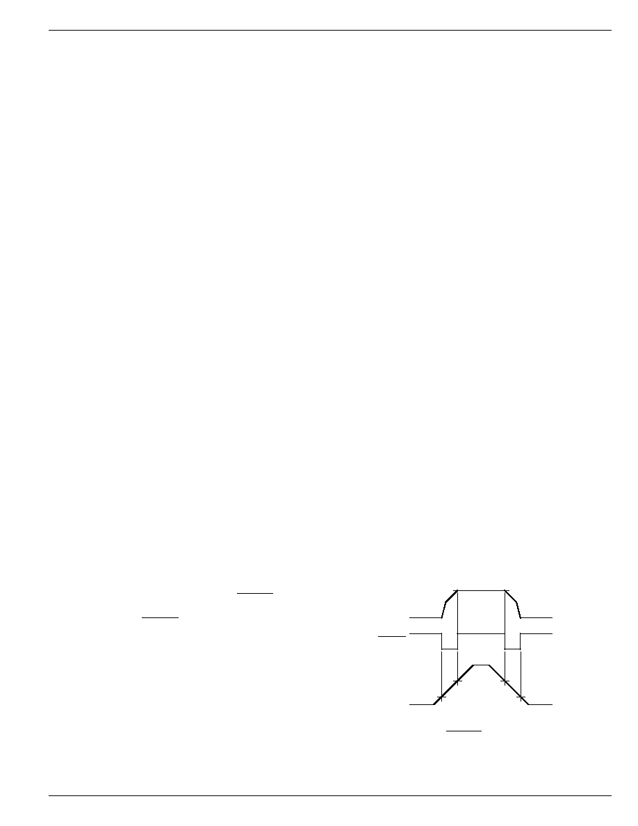
Figure 1 is a timing diagram depicting the ERROR signal and
the regulated output voltage as the MIC29371 input is ramped
up and down. The ERROR signal becomes valid (low) at
about 1.3V input. It goes high at about 5V input (the input
voltage at which V
OUT
= 4.75). Since the MIC29371's dropout
voltage is load-dependent (see curve in Typical Performance
Characteristics), the input voltage trip point (about 5V) will
vary with the load current. The output voltage trip point
(approximately 4.75V) does not vary with load.
* SEE APPLICATIONS INFORMATION
*
*
OUTPUT
VOLTAGE
INPUT
VOLTAGE
ERROR
NOT
VALID
NOT
VALID
5V
1.3V
4.75V
Figure 1. ERROR Output Timing
The error comparator has an NPN open-collector output
which requires an external pull-up resistor. Depending on
system requirements, this resistor may be returned to the 5V
output or some other supply voltage. In determining a value
for this resistor, note that while the output is rated to sink
250
µ
A, this sink current adds to battery drain in a low battery
condition. Suggested values range from 100k to 1M
. The
resistor is not required if this output is unused.
Programming the Output Voltage (MIC29372)
The MIC29372 may programmed for any output voltage
between its 1.235V reference and its 26V maximum rating. An
external pair of resistors is required, as shown in Figure 3.
The complete equation for the output voltage is
V
OUT
= V
REF
x { 1 + R
1
/R
2
} ≠
|
I
FB
|
R
1
where V
REF
is the nominal 1.235 reference voltage and I
FB
is
the Adjust pin bias current, nominally 20nA. The minimum
recommended load current of 1
µ
A forces an upper limit of
1.2M
on the value of R
2
, if the regulator must work with no
load (a condition often found in CMOS in standby), I
FB
will
produce a ≠2% typical error in V
OUT
which may be eliminated
at room temperature by trimming R
1
. For better accuracy,
choosing R
2
= 100k reduces this error to 0.17% while increasing
the resistor program current to 12
µ
A. Since the MIC29372
typically draws 100
µ
A at no load with SHUTDOWN open-
circuited, this is a negligible addition.
Reducing Output Noise
In reference applications it may be advantageous to reduce
the AC noise present at the output. One method is to reduce
the regulator bandwidth by increasing the size of the output
capacitor. This is relatively inefficient, as increasing the
capacitor from 1
µ
F to 220
µ
F only decreases the noise from
430
µ
V to 160
µ
V
RMS
for a 100kHz bandwidth at 5V output.
Noise can be reduced by a factor of four with the adjustable
MIC2937A/29371/29372
Micrel
MIC2937A/29371/29372
26
October 1999
Automotive Applications
The MIC2937A is ideally suited for automotive applications
for a variety of reasons. It will operate over a wide range of
input voltages with very low dropout voltages (40mV at light
loads), and very low quiescent currents (100
µ
A typical).
These features are necessary for use in battery powered
systems, such as automobiles. It is a "bulletproof" device with
the ability to survive both reverse battery (negative transients
up to 20V below ground), and load dump (positive transients
up to 60V) conditions. A wide operating temperature range
with low temperature coefficients is yet another reason to use
these versatile regulators in automotive designs.
OUT
GND
+VIN
*V
5V
OUT
V
V
10µF
+
IN
V
OUT
= 5V
Figure 2. MIC2937A-5.0 Fixed +5V Regulator
Figure 3. MIC29372 Adjustable Regulator
Typical Applications
Figure 5. MIC29372 5.0V or 3.3V Selectable Regulator with
Shutdown.
Figure 4. MIC29372 Wide Input Voltage Range Current Limiter
*MINIMUM INPUT-OUTPUT VOLTAGE RANGES FROM 40
m
V TO 400
m
V,
DEPENDING ON LOAD CURRENT.
SHUTDOWN PIN LOW= ENABLE OUTPUT. Q1 ON = 3.3V, Q1 OFF = 5.0V.
SHUTDOWN
V
GND
OUT
+VIN
ADJUST
SHUTDOWN
INPUT
100pF
2N2222
1%
300k
+5V to +7V
1%
180k
+
10µF
470 k
OFF
ON
5V
3.3V
220k
1%
VCC OUT
Input
Output
0
3.3V
1
5.0V
OUT
GND
ADJUST
V
VIN
+VIN
VOUT
VIN
C
BYPASS
1
2 R
1
∑ 200 Hz
regulators with a bypass capacitor across R
1
, since it reduces
the high frequency gain from 4 to unity. Pick
or about 0.01
µ
F. When doing this, the output capacitor must
be increased to 10
µ
F to maintain stability. These changes
reduce the output noise from 430
µ
V to 100
µ
V
RMS
for a 100
kHz bandwidth at 5V output. With the bypass capacitor
added, noise no longer scales with output voltage so that
improvements are more dramatic at higher output voltages.
IN
OUT
GND ADJUST
SHUTDOWN
V
V
SHUTDOWN
INPUT
OUT
V
1.2V
26V
1
R
.01
µF
10µF
2
R
1.23V
REF
V
VOUT = VREF x (1 + )
1
R
2
R
OFF
ON