MIC2950/2951
Micrel
February 1999
1
MIC2950/2951
MIC2950/2951
150mA Low-Dropout Voltage Regulator
Block Diagram
60mV
1.23V
REF.
Error
Amp.
Error Detection
Comparator
182k
60k
1.5µF
SNS
TAP
ERR
GND
OUT
5V/150mA
Output
TTL/CMOS
Compatible
Error Output
IN
FB
Unregulated
DC Supply
TTL/CMOS
Control Logic
Input
SHDN
330k
MIC2951-0x
General Description
The MIC2950 and MIC2951 are "bulletproof" micropower
voltage regulators with very low dropout voltage (typically
40mV at light loads and 250mV at 100mA), and very low
quiescent current. Like their predecessors, the LP2950 and
LP2951, the quiescent current of the MIC2950/MIC2951
increases only slightly in dropout, thus prolonging battery life.
The MIC2950/MIC2951 are pin for pin compatible with the
LP2950/LP2951, but offer lower dropout, lower quiescent
current, reverse battery, and automotive load dump protection.
The key additional features and protection offered include
higher output current (150mA), positive transient protection
for up to 60V (load dump), and the ability to survive an
unregulated input voltage transient of ≠20V below ground
(reverse battery).
The plastic DIP and SOIC versions offer additional system
functions such as programmable output voltage and logic
controlled shutdown. The 3-pin TO-92 MIC2950 is pin-
compatible with the older 5V regulators.
These system functions also include an error flag output that
warns of a low output voltage, which is often due to failing
batteries on the input. This may also be used as a power-on
reset. A logic-compatible shutdown input is also available
which enables the regulator to be switched on and off. This
part may also be pin-strapped for a 5 V output, or programmed
from 1.24 V to 29 V with the use of two external resistors.
Features
∑
High accuracy 3.3, 4.85, or 5V, guaranteed 150mA output
∑
Extremely low quiescent current
∑
Low-dropout voltage
∑
Extremely tight load and line regulation
∑
Very low temperature coefficient
∑
Use as regulator or reference
∑
Needs only 1.5
µ
F for stability
∑
Current and thermal limiting
∑
Unregulated DC input can withstand ≠20V reverse battery
and +60V positive transients
∑
Error flag warns of output dropout (MIC2951)
∑
Logic-controlled electronic shutdown (MIC2951)
∑
Output programmable from 1.24V to 29V (MIC2951)
Applications
∑
Automotive Electronics
∑
Battery Powered Equipment
∑
Cellular Telephones
∑
SMPS Post-Regulator
∑
Voltage Reference
∑
Avionics
∑
High Efficiency Linear Power Supplies
Micrel, Inc. ∑ 1849 Fortune Drive ∑ San Jose, CA 95131 ∑ USA ∑ tel + 1 (408) 944-0800 ∑ fax + 1 (408) 944-0970 ∑ http://www.micrel.com
MIC2950/2951
Micrel
MIC2950/2951
2
February 1999
Pin Description
Pin #
Pin #
Pin Name
Pin Function
MIC2950
MIC2951
3
1
OUT
Regulated Output
2
SNS
Sense (Input): Output-voltage sensing end of internal voltage divider for
fixed 5V operation. Not used in adjustable configuration.
3
SHDN
Shutdown/Enable (Input): TTL compatible input. High = shutdown,
low or open = enable.
2
4
GND
Ground
5
ERR
Error Flag (Output): Active low, open-collector output (low = error,
floating = normal).
6
TAP
3.3V/4.85/5V Tap: Output of internal voltage divider when the regulator is
configured for fixed operation. Not used in adjustable configuration.
7
FB
Feedback (Input): 1.235V feedback from internal voltage divider's TAP (for
fixed operation) or external resistor network (adjustable configuration).
1
8
IN
Unregulated Supply Input
Pin Configuration
1
2
3
4
8
7
6
5
IN
FB
TAP
ERR
OUT
SNS
SHDN
GND
MIC2951-xx
DIP (N), SOIC (M), MM8TM (MM)
(Top View)
3
2
1
OUT
GND
IN
MIC2950-xx
TO-92 (Z)
(Bottom View)
Ordering Information
Part Number
Voltage
Accuracy Temperature Range*
Package
MIC2950-05BZ
5.0V
0.5%
≠40
∞
C to +125
∞
C
TO-92
MIC2950-06BZ
5.0V
1.0%
≠40
∞
C to +125
∞
C
TO-92
MIC2951-02BM
5.0V
0.5%
≠40
∞
C to +125
∞
C
8-pin SOIC
MIC2951-03BM
5.0V
1.0%
≠40
∞
C to +125
∞
C
8-pin SOIC
MIC2951-02BN
5.0V
0.5%
≠40
∞
C to +125
∞
C
8-pin plastic DIP
MIC2951-03BN
5.0V
1.0%
≠40
∞
C to +125
∞
C
8-pin plastic DIP
MIC2951-03BMM
5.0V
1.0%
≠40
∞
C to +125
∞
C
8-lead MM8TM
MIC2951-3.3BM
3.3V
1.0%
≠40
∞
C to +125
∞
C
8-pin SOIC
MIC2951-4.8BM
4.85V
1.0%
≠40
∞
C to +125
∞
C
8-pin SOIC
* junction temperature
The MIC2950 is available as either an -05 or -06 version. The
-05 and -06 versions are guaranteed for junction temperatures
from ≠40
∞
C to +125
∞
C; the -05 version has a tighter output and
reference voltage specification range over temperature. The
MIC2951 is available as an -02 or -03 version.
The MIC2950 and MIC2951 have a tight initial tolerance
(0.5% typical), a very low output voltage temperature coefficient
which allows use as a low-power voltage reference, and
extremely good load and line regulation (0.04% typical). This
greatly reduces the error in the overall circuit, and is the result
of careful design techniques and process control.
MIC2950/2951
Micrel
February 1999
3
MIC2950/2951
Electrical Characteristics
(Note 16)
V
IN
= 6V; I
L
= 100
µ
A; C
L
= 1
µ
F; T
J
= 25
∞
C, bold values indicate ≠40
∞
C
T
J
+125
∞
C; Note 8; unless noted.
Parameter
Condition
Min
Typ
Max
Units
Output Voltage
MIC295x-02/-05 (
±
0.5%), T
J
= 25
∞
C
4.975
5.000
5.025
V
MIC295x-03/-06 (
±
1%), T
J
= 25
∞
C
4.950
5.000
5.050
V
MIC2951-3.3 (
±
1%), T
J
= 25
∞
C
3.267
3.300
3.333
V
MIC2951-4.8 (
±
1%), T
J
= 25
∞
C
4.802
4.850
4.899
V
Output Voltage
MIC295x-02/-05 (
±
0.5%), ≠25
∞
C
T
J
+85
∞
C
4.950
5.050
V
MIC295x-03/-06 (
±
1%), ≠25
∞
C
T
J
+85
∞
C
4.925
5.075
V
MIC2951-3.3 (
±
1%), ≠25
∞
C
T
J
+85
∞
C
3.251
3.350
V
MIC2951-4.8 (
±
1%), ≠25
∞
C
T
J
+85
∞
C
4.777
4.872
V
Output Voltage
MIC295x-02/-05 (
±
0.5%), ≠40
∞
C to +125
∞
C
4.940
5.060
V
Over Full Temperature Range
MIC295x-03/-06 (
±
1%), ≠40
∞
C to +125
∞
C
4.900
5.100
V
MIC2951-3.3 (
±
1%), ≠40
∞
C to +125
∞
C
3.234
3.366
V
MIC2951-4.8 (
±
1%), ≠40
∞
C to +125
∞
C
4.753
4.947
V
Output Voltage
MIC295x-02/-05 (
±
0.5%), 100
µ
A
I
L
150mA, T
J
T
J(max)
4.930
5.070
V
Over Load Variation
MIC295x-03/-06 (
±
1%), 100
µ
A
I
L
150mA, T
J
T
J(max)
4.880
5.120
V
MIC2951-3.3 (
±
1%), 100
µ
A
I
L
150mA, T
J
T
J(max)
3.221
3.379
V
MIC2951-4.8 (
±
1%), 100
µ
A
I
L
150mA, T
J
T
J(max)
4.733
4.967
V
Output Voltage
MIC295x-02/-05 (
±
0.5%), Note 9
20
100
ppm/
∞
C
Temperature Coefficient
MIC295x-03/-06 (
±
1%), Note 9
50
150
ppm/
∞
C
MIC2951-3.3 (
±
1%), Note 9
50
150
ppm/
∞
C
MIC2951-4.8 (
±
1%), Note 9
50
150
ppm/
∞
C
Line Regulation
MIC295x-02/-05 (
±
0.5%), Note 10, 11
0.03
0.10
%
0.20
%
MIC295x-03/-06 (
±
1%), Note 10, 11
0.04
0.20
%
0.40
%
MIC2951-3.3 (
±
1%), Note 10, 11
0.04
0.20
%
0.40
%
MIC2951-4.8 (
±
1%), Note 10, 11
0.04
0.20
%
0.40
%
Absolute Maximum Ratings
(Note 1)
Input Suppy Voltage (V
IN
) Note 5 ................. ≠20V to +60V
Feedback Input Voltage (V
FB
) Note 6, 7 ...... ≠1.5V to +26V
Shutdown Input Voltage (V
SHDN
) Note 6 ..... ≠0.3V to +30V
Power Dissipation (P
D
) Note 4 ................ Internally Limited
Storage Temperature .............................. ≠65
∞
C to + 150
∞
C
Lead Temperature (soldering, 5 sec.) ....................... 260
∞
C
ESD, Note 3
Operating Ratings
(Note 2)
Input Supply Voltage (V
IN
) ........................... +2.0V to +30V
Junction Temperature (T
J
) ....................................... Note 4
MIC2950-05/MIC2950-06 ..................... ≠40
∞
C to +125
∞
C
MIC2951-02/MIC2950-03 ..................... ≠40
∞
C to +125
∞
C

MIC2950/2951
Micrel
MIC2950/2951
4
February 1999
Parameter
Condition
Min
Typ
Max
Units
Load Regulation
MIC295x-02/-05 (
±
0.5%), 100
µ
A
I
L
150mA, Note 10
0.04
0.10
%
0.20
%
MIC295x-03/-06 (
±
1%), 100
µ
A
I
L
150mA, Note 10
0.10
0.20
%
0.30
%
MIC2951-3.3 (
±
1%), 100
µ
A
I
L
150mA, Note 10
0.10
0.20
%
0.30
%
MIC2951-4.8 (
±
1%), 100
µ
A
I
L
150mA, Note 10
0.10
0.20
%
0.30
%
Dropout Voltage
MIC295x-02/-03/-05/-06, I
L
= 100
µ
A, Note 12
40
80
mV
140
mV
MIC295x-02/-03/-05/-06, I
L
= 100mA, Note 12
250
300
mV
MIC295x-02/-03/-05/-06, I
L
= 150mA, Note 12
300
450
mV
600
mV
MIC2951-3.3 (
±
1%), I
L
= 100
µ
A, Note 12
40
80
mV
150
mV
MIC2951-3.3 (
±
1%), I
L
= 100mA, Note 12
250
350
mV
MIC2951-3.3 (
±
1%), I
L
= 150mA, Note 12
320
450
mV
600
mV
MIC2951-4.8 (
±
1%), I
L
= 100
µ
A, Note 12
40
80
mV
140
mV
MIC2951-4.8 (
±
1%), I
L
= 100mA, Note 12
250
300
mV
MIC2951-4.8 (
±
1%), I
L
= 150mA, Note 12
300
450
mV
600
mV
Ground Current
MIC295x-02/-03/-05/-06, I
L
= 100
µ
A
120
180
µ
A
300
µ
A
MIC295x-02/-03/-05/-06, I
L
= 100mA
1.7
2.5
mA
3.5
mA
MIC295x-02/-03/-05/-06, I
L
= 150mA
4
6
mA
8
mA
MIC2951-3.3 (
±
1%), I
L
= 100
µ
A
100
180
µ
A
300
µ
A
MIC2951-3.3 (
±
1%), I
L
= 100mA
1.7
2.5
mA
MIC2951-3.3 (
±
1%), I
L
= 150mA
4
6
mA
10
mA
MIC2951-4.8 (
±
1%), I
L
= 100
µ
A
120
180
µ
A
300
µ
A
MIC2951-4.8 (
±
1%), I
L
= 100mA
1.7
2.5
mA
3.5
mA
MIC2951-4.8 (
±
1%), I
L
= 150mA
4
6
mA
8
mA
Dropout Ground Current
MIC295x-02/-03/-05/-06 (
±
0.5%), V
IN
= 4.5V, I
L
= 100
µ
A
280
350
µ
A
400
µ
A
MIC2951-3.3 (
±
1%), V
IN
= 3.0V, I
L
= 100
µ
A
150
350
µ
A
400
µ
A
MIC2951-4.8 (
±
1%), V
IN
= 4.3V, I
L
= 100
µ
A
280
350
µ
A
400
µ
A
MIC2950/2951
Micrel
February 1999
5
MIC2950/2951
Parameter
Condition
Min
Typ
Max
Units
Current Limit
V
OUT
= 0V
300
400
mA
450
mA
Thermal Regulation
Note 13
0.05
0.20
%/W
Output Noise
10Hz to 100kHz, C
L
= 1.5
µ
F
430
µ
V
RMS
10Hz to 100kHz, C
L
= 200
µ
F
160
µ
V
RMS
10Hz to 100kHz, C
L
= 3.3
µ
F,
100
µ
V
RMS
0.01
µ
F bypass Feedback to Output
Reference Voltage
MIC295x-02/-05 (
±
0.5%)
1.220
1.235
1.250
V
1.200
1.260
V
MIC295x-03/-06 (
±
1%)
1.210
1.235
1.260
V
1.200
1.270
V
MIC2951-3.3 (
±
1%)
1.210
1.235
1.260
V
1.200
1.270
V
MIC2951-4.8 (
±
1%)
1.210
1.235
1.260
V
1.200
1.270
V
Reference Voltage
MIC295x-02/-05 (
±
0.5%), Note 14
1.190
1.270
V
MIC295x-03/-06 (
±
1%), Note 14
1.185
1.285
V
MIC2951-3.3 (
±
1%), Note 14
1.185
1.285
V
MIC2951-4.8 (
±
1%), Note 14
1.185
1.285
V
Feedback Bias Current
20
40
nA
60
nA
Reference Voltage
MIC295x-02/-05 (
±
0.5%), Note 9
20
ppm/
∞
C
Temperature Coefficient
MIC295x-03/-06 (
±
1%), Note 9
50
ppm/
∞
C
MIC2951-3.3 (
±
1%), Note 9
50
ppm/
∞
C
MIC2951-4.8 (
±
1%), Note 9
50
ppm/
∞
C
Feedback Bias Current
0.1
nA/
∞
C
Temperature Coefficient
Error Comparator (Flag)
V
OH
= 30V
0.01
1.00
µ
A
Output Leakage Current
2.00
µ
A
Error Comparator (Flag)
V
IN
= 4.5V, I
OL
= 200
µ
A
150
250
mV
Output Low Voltage
400
mV
Error Comparator
Note 15
40
60
mV
Upper Threshold Voltage
25
mV
Error Comparator
Note 15
75
95
mV
Lower Threshold Voltage
140
mV
Error Comparator Hysteresis
Note 15
15
mV
MIC2950/2951
Micrel
MIC2950/2951
6
February 1999
Parameter
Condition
Min
Typ
Max
Units
Shutdown Input Logic Voltage
MIC295x-02/-05 (
±
0.5%)
1.3
V
Low
0.7
V
High
2.0
V
MIC295x-03/-06 (
±
1%)
1.3
V
Low
0.7
V
High
2.0
V
MIC2951-3.3 (
±
1%)
1.3
V
Low
0.7
V
High
2.0
V
MIC2951-4.8 (
±
1%)
1.3
V
Low
0.7
V
High
2.0
V
Shutdown Input Current
V
SHUTDOWN
= 2.4V
30
50
µ
A
100
µ
A
V
SHUTDOWN
= 30V
450
600
µ
A
750
µ
A
Regulator Output Current
Note 7
3
10
µ
A
in Shutdown
20
µ
A
Note 1.
Exceeding the absolute maximum rating may damage the device.
Note 2.
The device is not guaranteed to function outside its operating rating.
Note 3.
Devices are ESD sensitive. Handling precautions are recommended.
Note 4.
The junction-to-ambient thermal resistance of the TO-92 package is 180
∞
C/W with 0.4" leads and 160
∞
C/W with 0.25" leads to a PC board.
The thermal resistance of the 8-pin DIP package is 105
∞
C/W junction-to-ambient when soldered directly to a PC board. Junction-to-ambient
thermal resistance for the SOIC (M) package is 160
∞
C/W. Junction-to-ambient thermal resistance for the MM8TM (MM) is 250
∞
C/W.
Note 5.
The maximum positive supply voltage of 60V must be of limited duration (
100ms) and duty cycle (
1%). The maximum continuous supply
voltage is 30V.
Note 6.
When used in dual-supply systems where the output terminal sees loads returned to a negative supply, the output voltage should be diode-
clamped to ground.
Note 7.
V
SHDN
2V, V
IN
30 V, V
OUT
= 0, with the FB pin connected to TAP.
Note 8.
Additional conditions for 8-pin devices are V
FB
= 5V, TAP and OUT connected to SNS (V
OUT
= 5V) and V
SHDN
0.8V.
Note 9.
Output or reference voltage temperature coefficient is defined as the worst case voltage change divided by the total temperature range.
Note 10. Regulation is measured at constant junction temperature, using pulse testing with a low duty cycle. Changes in output voltage due to heating
effects are covered in the specification for thermal regulation.
Note 11. Line regulation for the MIC2951 is tested at 150
∞
C for I
L
= 1mA. For I
L
= 100
µ
A and T
J
= 125
∞
C, line regulation is guaranteed by design to
0.2%. See Typical Performance Characteristics for line regulation versus temperature and load current.
Note 12. Dropout voltage is defined as the input to output differential at which the output voltage drops 100mV below its nominal value measured at 1V
differential. At very low values of programmed output voltage, the minimum input supply voltage of 2V (2.3V over temperature) must be taken
into account.
Note 13. Thermal regulation is defined as the change in output voltage at a time "t" after a change in power dissipation is applied, excluding load or line
regulation effects. Specifications are for a 50mA load pulse at V
IN
= 30V (1.25W pulse) for t = 10ms.
Note 14. V
REF
V
OUT
(V
IN
≠ 1 V), 2.3V
V
IN
30V, 100
µ
A < I
L
150mA, T
J
T
JMAX
.
Note 15. Comparator thresholds are expressed in terms of a voltage differential at the FB terminal below the nominal reference voltage measured at 6V
input. To express these thresholds in terms of output voltage change, multiply by the error amplifier gain = V
OUT
/V
REF
=
(R1 + R2)/R2. For example, at a programmed output voltage of 5V, the error output is guaranteed to go low when the output drops by
95mV x 5V/1.235V = 384mV. Thresholds remain constant as a percent of V
OUT
as V
OUT
is varied, with the dropout warning occurring at
typically 5% below nominal, 7.5% guaranteed.
Note 16. Specification for packaged product only.
MIC2950/2951
Micrel
February 1999
7
MIC2950/2951
Typical Characteristics
Ground Pin Current
Dropout Characteristics
Input Current
Ground Pin Current
Output Voltage vs.
Temperature of 3
Representative Units
Input Current
Ground Pin Current
Ground Pin Current
Ground Pin Current
Dropout Voltage
Short Circuit Current
Dropout Voltage
0.1
1
10
150
10
1
0.1
0.01
0
1
2
3
4
5
6
1
2
3
4
5
6
0
0
50
100
150
200
250
300
350
400
0
1 2
3 4
5 6
7 8 9 10
120
110
100
90
80
70
60
50
40
30
20
10
0
0
1
2
3
4
5
6 7
8
9 10
5.06
5.04
5.02
5.0
4.98
4.96
4.94
-75 -50 -25 0 25 50 75 100 125 150
0
20
40
60
80
100
120
140
180
0
1
2
3
4
5
6
7
8
350
300
250
200
150
100
50
0
-75 -50 -25 0 25 50 75 100 125 150
7
6
5
4
-75 -50 -25 0 25 50 75 100 125 150
9
7
5
3
0
0
1
2
3
4
5
6
7
8
450
400
350
300
250
200
150
100
-75 -50 -25 0 25 50 75 100 125 150
600
500
400
300
100
50
0
-75 -50 -25 0 25 50 75 100 125 150
500
400
300
200
100
0
0.1
1
10
100
R = 50k
L
R = 33
L
0.2%
V = 6V
I = 100
µ
A
IN
L
V = 6V
I = 150 mA
IN
L
I = 150 mA
L
I = 100
µ
A
L
T = 25
∞
C
J
LOAD CURRENT (mA)
INPUT VOLTAGE (V)
INPUT VOLTAGE (V)
INPUT VOLTAGE (V)
TEMPERATURE (
∞
C)
INPUT VOLTAGE (V)
TEMPERATURE (
∞
C)
TEMPERATURE (
∞
C)
INPUT VOLTAGE (V)
TEMPERATURE (
∞
C)
TEMPERATURE (
∞
C)
OUTPUT CURRENT (mA)
QUIESCENT CURRENT
OUTPUT VOLTAGE (V)
INPUT CURRENT (
µ
A)
INPUT CURRENT (mA)
OUTPUT VOLTAGE (V)
QUIESCENT CURRENT (
µ
A)
QUIESCENT CURRENT (
µ
A)
QUIESCENT CURRENT (mA)
QUIESCENT CURRENT (mA)
SHORT CIRCUIT CURRENT (mA)
DROPOUT VOLTAGE (mV)
DROPOUT VOLTAGE (mV)
R =
L
130
140
150
160
L
R = 50
R = 50k
L
I = 1 mA
L
I = 0
L
I = 150 mA
L
150
MIC2950/2951
Micrel
MIC2950/2951
8
February 1999
MIC2951
Error Comparator Output
MIC2951
Minimum Operating Voltage
Line Transient Response
Load Transient Response
Load Transient Response
Ripple Rejection
Output Impedance
2.2
2.0
1.9
1.6
-30
-20
-10
0
10
20
-250
-200
-150
-100
-50
0
50
-2.0 -1.5 -1.0 -0.5
0
0.5
1.0
8
6
4
2
0
-2
0
1
2
3
4
6
5
2.5
2.0
1.5
1.0
0.5
0.0
0
200
mV
400
mV
0
200
400
600
800
125
100
75
50
25
0
-25
-50
0
2
4
6
8
10
80
0
4
8
12
16
20
7
6
5
4
3
2
1
0
-100 0 100 200 300 400 500 600 700
10
5
2
1
0.5
0.2
0.1
0.05
10
100
1K
10K 100K
1M
90
80
70
60
50
40
20
10
10
70
60
50
40
30
20
T = 125
∞
C
A
C = 4.7
µ
F
V = 5V
L
OUT
I = 10 mA
V = 8V
V = 5V
L
I = 0
L
I = 100
µ
A
L
TEMPERATURE (
∞
C)
FEEDBACK VOLTAGE (V)
TIME (
µ
S)
OUTPUT LOW VOLTAGE (V)
INPUT VOLTAGE (V)
TIME (mS)
TIME (mS)
FREQUENCY (Hz)
FREQUENCY (Hz)
MINIMUM OPERATING VOLTAGE (V)
BIAS CURRENT (nA)
FEEDBACK CURRENT (
µ
A)
COMPARATOR OUTPUT (V)
SINK CURRENT (mA)
OUTPUT VOLTAGE
CHANGE (mV)
OUTPUT IMPEDANCE (OHMS)
RIPPLE REJECTION (dB)
RIPPLE REJECTION (dB)
MIC2951
Feedback Bias Current
MIC2951
Feedback Pin Current
MIC2951
Comparator Sink Current
MIC2951
Enable Transient
Ripple Rejection
2.1
1.8
1.7
-75 -50 -25 0 25 50 75 100 125 150
-75 -50 -25 0 25 50 75 100 125 150
TEMPERATURE (
∞
C)
PIN 7 DRIVEN BY EXTERNAL
SOURCE (REGULATOR RUN
OPEN LOOP)
T = 25
∞
C
A
V = 5V
OUT
T = 125
∞
C
A
T = 25
∞
C
A
T = -55
∞
C
A
0.0 0.1 0.2 0.3 0.4 0.5 0.6 0.7 0.8 0.9
-50
mV
8V
6V
4V
100
mA
100
µ
A
LOAD
CURRENT
C = 4.7
µ
F
I = 1 mA
V = 5V
L
OUT
L
60
40
20
0
-20
-40
-60
100
mA
100
µ
A
OUTPUT VOLTAGE
CHANGE (mV)
LOAD
CURRENT
C = 15
µ
F
V = 5V
L
OUT
OUTPUT VOLTAGE
CHANGE
INPUT
VOLTAGE
OUTPUT
VOLTAGE (V)
SHUTDOWN
PIN VOLTAGE (V)
2
0
-2
C = 10
µ
F
L
IN
OUT
0.02
0.01
I = 100
µ
A
0
I = 1 mA
0
I = 100 mA
0
V = 5V
C = 4.7
µ
F
L
OUT
30
10
10
10
10
1
3
4
6
C = 1.5
µ
F
V = 6V
V = 5V
L
IN
OUT
C = 1.5
µ
F
V = 6V
V = 5V
L
IN
OUT
I = 10 mA
L
I = 1 mA
L
80
90
HYSTERESIS
PULLUP RESISTOR TO
SEPARATE 5V SUPPLY
2
10
10
FREQUENCY (Hz)
10
10
10
10
1
2
3
4
5
6
T = ≠55
∞
C
A
TIME (
µ
S)
C = 1.5
µ
F
L
MIC2950/2951
Micrel
February 1999
9
MIC2950/2951
120
100
80
60
40
20
0
130
140
150
0
Ripple Rejection
Shutdown Threshold Voltage
80
70
60
50
40
30
20
10
10
10
10
10
10
10
1
2
3
4
5
6
0.6
0.8
1.0
1.2
1.4
1.6
1.8
-75 -50 -25 0 25 50 75 100 125 150
FREQUENCY (Hz)
TEMPERATURE (
∞
C)
3.5
3.0
2.5
2.0
1.5
1.0
0.5
0.0
30
25
20
0
10
0
-10
400
300
200
100
0
5
10
15
20
25
30
0
5
10
15
20
25
30
10
10
10
10
2
3
4
5
-75 -50 -25 0 25 50 75 100 125 150
Output Noise
MIC2951 Divider Resistance
Line Regulation
MIC2951 Maximum
Rated Output Current
15
10
5
5
-5
FREQUENCY (Hz)
TEMPERATURE (
∞
C)
RIPPLE REJECTION (dB)
VOLTAGE NOISE
SPECTRAL DENSITY (
µ
V/ Hz)
PIN 2 TO PIN 4 RESISTANCE (k )
SHUTDOWN THRESHOLD VOLTAGE (V)
INPUT VOLTAGE (V)
INPUT VOLTAGE (V)
OUTPUT VOLTAGE CHANGE (mV)
OUTPUT CURRENT (mA)
I = 50
µ
A
L
C = 1.5
µ
F
V = 6V
V = 5V
IN
L
OUT
0.01
µ
F
BYPASS
PIN 1 TO
PIN 7
C = 220
µ
F
I = 100 mA
L
L
C = 4.7
µ
F
L
C =
3.3
µ
F
L
I = 100
µ
A
L
I = 1 mA
L
I = 100
µ
A
L
T = 150
∞
C
J
T = 125
∞
C
J
T = 125
∞
C
J
MAX
V = 5V
OUT
T = 25
∞
C
A
T = 50
∞
C
A
T = 85
∞
C
A
8-PIN SOIC
SOLDERED
TO PC BOARD
I = 100 mA
L
OUTPUT CURRENT (mA)
A
5
4
2
0
-2
1
-1
0
0
10
20
50
30
40
Thermal Response
POWER
DISSIPATION (W)
OUTPUT VOLTAGE
CHANGE (mV)
1.25W
TIME (
µ
S)
J
MAX
A
TO-92 PACKAGE
.25" LEADS SOLDERED
TO PC BOARD
T = 125
∞
C
T = 25
∞
C
T = 85
∞
C
120
100
80
60
40
20
0
130
140
150
0
0
5
10
15
20
30
25
MIC2950 Maximum
Rated Output
INPUT VOLTAGE (V)
0
1
2
5
3
4
Fold-Back Current Limiting
OUTPUT CURRENT (mA)
OUTPUT VOLTAGE (V)
600
500
400
300
100
200

MIC2950/2951
Micrel
MIC2950/2951
10
February 1999
offset of about 60mV divided by the 1.235V reference voltage.
(Refer to the block diagram on Page 1). This trip level remains
"5% below normal" regardless of the programmed output
voltage of the MIC2951. For example, the error flag trip level
is typically 4.75V for a 5V output or 11.4V for a 12V output. The
out of regulation condition may be due either to low input
voltage, current limiting, thermal limiting, or overvoltage on
input (over
40V).
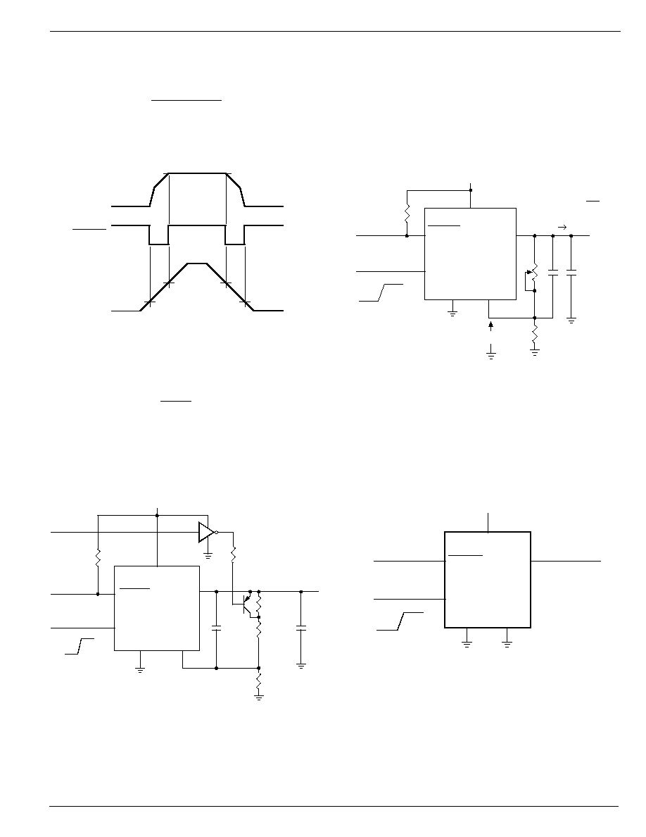
Figure 1 is a timing diagram depicting the ERROR signal and
the regulated output voltage as the MIC2951 input is ramped
up and down. The ERROR signal becomes valid (low) at
about 1.3V input. It goes high at about 5V input (the input
voltage at which V
OUT
= 4.75--for 5.0V applications). Since
the MIC2951's dropout voltage is load-dependent (see curve
in Typical Performance Characteristics), the input voltage trip
point (about 5V) will vary with the load current. The output
voltage trip point does not vary with load.
The error comparator has an open-collector output which
requires an external pull-up resistor. Depending on system
requirements, this resistor may be returned to the output or
some other supply voltage. In determining a value for this
resistor, note that while the output is rated to sink 200
µ
A, this
sink current adds to battery drain in a low battery condition.
Suggested values range from 100k to 1M
. The resistor is not
required if this output is unused.
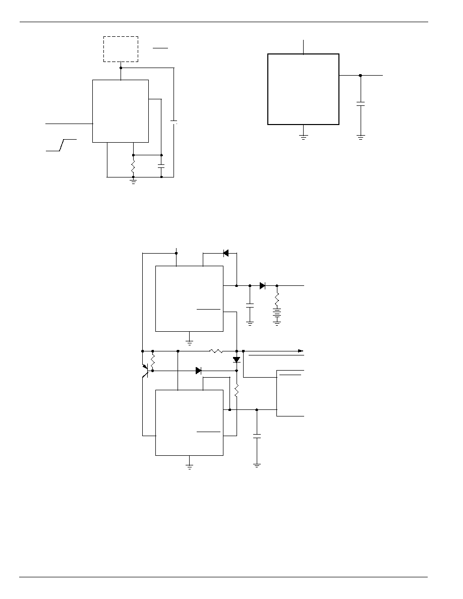
Programming the Output Voltage (MIC2951)
The MIC2951 may be pin-strapped for 5V (or 3.3V or 4.85V)
using its internal voltage divider by tying Pin 1 (output) to Pin
2 (sense) and Pin 7 (feedback) to Pin 6 (5V Tap). Alternatively,
it may be programmed for any output voltage between its
1.235V reference and its 30V maximum rating. An external
pair of resistors is required, as shown in Figure 2.
The complete equation for the output voltage is
V
OUT
= V
REF
x { 1 + R
1
/R
2
} + I
FB
R
1
where V
REF
is the nominal 1.235 reference voltage and I
FB
is
the feedback pin bias current, nominally ≠20nA. The minimum
recommended load current of 1
µ
A forces an upper limit of
1.2M
on the value of R
2
, if the regulator must work with no
load (a condition often found in CMOS in standby), I
FB
will
produce a 2% typical error in V
OUT
which may be eliminated
at room temperature by trimming R
1
. For better accuracy,
choosing R
2
= 100k reduces this error to 0.17% while
increasing the resistor program current to 12
µ
A.
Reducing Output Noise
In some applications it may be advantageous to reduce the
AC noise present at the output. One method is to reduce the
regulator bandwidth by increasing the size of the output
capacitor. This is the only method by which noise can be
reduced on the 3 lead MIC2950 and is relatively inefficient, as
increasing the capacitor from 1
µ
F to 220
µ
F only decreases
the noise from 430
µ
V to 160
µ
V rms for a 100kHz bandwidth
at 5V output.
Applications Information
Automotive Applications
The MIC2950/2951 are ideally suited for automotive
applications for a variety of reasons. They will operate over a
wide range of input voltages, have very low dropout voltages
(40mV at light loads), and very low quiescent currents. These
features are necessary for use in battery powered systems,
such as automobiles. They are also "bulletproof" devices; with
the ability to survive both reverse battery (negative transients
up to 20V below ground), and load dump (positive transients
up to 60V) conditions. A wide operating temperature range
with low temperature coefficients is yet another reason to use
these versatile regulators in automotive designs.
External Capacitors
A 1.5
µ
F (or greater) capacitor is required between the
MIC2950/MIC2951 output and ground to prevent oscillations
due to instability. Most types of tantalum or aluminum
electrolytics will be adequate; film types will work, but are
costly and therefore not recommended. Many aluminum
electrolytics have electrolytes that freeze at about ≠30
∞
C, so
solid tantalums are recommended for operation below ≠25
∞
C.
The important parameters of the capacitor are an effective
series resistance of about 5
or less and a resonant frequency
above 500kHz. The value of this capacitor may be increased
without limit.
At lower values of output current, less output capacitance is
required for output stability. The capacitor can be reduced to
0.5
µ
F for current below 10mA or 0.15
µ
F for currents below 1
mA. Using the 8-pin versions at voltages below 5V runs the
error amplifier at lower gains so that more output capacitance
is needed. For the worst-case situation of a 150mA load at
1.23V output (Output shorted to Feedback) a 5
µ
F (or greater)
capacitor should be used.
The MIC2950 will remain stable and in regulation with no load
in addition to the internal voltage divider, unlike many other
voltage regulators. This is especially important in CMOS RAM
keep-alive applications. When setting the output voltage of
the MIC2951 version with external resistors, a minimum load
of 1
µ
A is recommended.
A 0.1
µ
F capacitor should be placed from the MIC2950/
MIC2951 input to ground if there is more than 10 inches of wire
between the input and the AC filter capacitor or if a battery is
used as the input.
Stray capacitance to the MIC2951 Feedback terminal (pin 7)
can cause instability. This may especially be a problem when
using high value external resistors to set the output voltage.
Adding a 100pF capacitor between Output and Feedback and
increasing the output capacitor to at least 3.3
µ
F will remedy
this.
Error Detection Comparator Output
A logic low output will be produced by the comparator whenever
the MIC2951 output falls out of regulation by more than
approximately 5%. This figure is the comparator's built-in
MIC2950/2951
Micrel
February 1999
11
MIC2950/2951
MIC2951
IN
OUT
GND
FB
ERROR
5
3
4
1
8
SD
V
V
ERROR
OUTPUT
SHUTDOWN
INPUT
IN
+V
100k
OUT
V
1.2
30V
1
R 100
pF
3.3µF
2
R
1.23V
REF
V
7
OUT
V
REF
= V
x (1 + )
1
R
2
R
OFF
ON
Noise can be reduced fourfold by a bypass capacitor across
R
1
, since it reduces the high frequency gain from 4 to unity.
Pick:
870 23
or about 0.01
µ
F. When doing this, the output capacitor must
be increased to 3.3
µ
F to maintain stability. These changes
reduce the output noise from 430
µ
V to 100
µ
V rms for a 100
kHz bandwidth at 5V output. With the bypass capacitor
added, noise no longer scales with output voltage so that
improvements are more dramatic at higher output voltages.
MIC2951
SD
V
ERROR
GND
4
7
8
OUT
+V IN
FB
1
5
3
ERROR
OUTPUT
SHUTDOWN
INPUT
47k
*SLEEP
INPUT
100pF
2N3906
200k
1%
100k
C-MOS
GATE
+V IN
1%
100k
+
3.3µF
+V OUT
470 k
OFF
ON
*HIGH INPUT LOWERS V
OUT
TO 2.5V
Typical Applications
870 25
*MINIMUM INPUT-OUTPUT VOLTAGE RANGES FROM 40
m
V TO 400
m
V,
DEPENDING ON LOAD CURRENT.
MIC2951
OUT
FB
SD
ERROR
5
1
3
7
GND
4
+VIN
8
+VIN
*V
VIN
OUT
V
ERROR
OUTPUT
SHUTDOWN
INPUT
OFF
ON
Wide Input Voltage Range Current Limiter
5V Regulator with 2.5V Sleep Function
Figure 1. ERROR Output Timing
Figure 2. Adjustable Regulator
NOTE: PINS 2 AND 6 ARE LEFT OPEN
*SEE APPLICATIONS
INFORMATION
* SEE APPLICATIONS INFORMATION
C
BYPASS
1
2 R
1
∑ 200 Hz
*
OUTPUT
VOLTAGE
INPUT
VOLTAGE
ERROR
NOT
VALID
NOT
VALID
5V
1.3V
4.75V
*
MIC2950/2951
Micrel
MIC2950/2951
12
February 1999
Low Drift Current Source
5-Volt Current Limiter
* MINIMUM INPUT-OUTPUT VOLTAGE RANGES FROM 40mV TO 400mV,
DEPENDING ON LOAD CURRENT.
870 27
870 29
MIC2950Z
OUT
GND
+V IN
*V
5V
OUT
V
5V BUS
1µF
+
MIC2951
FB
SD
1
3
7
GND
4
VIN
8
OUT
V
SHUTDOWN
INPUT
LOAD
+V = 2
30V
I L
I L=
1.23V
R
0.1µF
1µF
1%
R
OFF
ON
Regulator with Early Warning and Auxiliary Output
∑ EARLY WARNING FLAG ON LOW INPUT VOLTAGE
∑ MAIN OUTPUT LATCHES OFF AT LOWER INPUT VOLTAGES
∑ BATTERY BACKUP ON AUXILIARY OUTPUT
OPERATION: REG. #1'S V
OUT
IS PROGRAMMED ONE DIODE DROP ABOVE 5 V.
ITS ERROR FLAG BECOMES ACTIVE WHEN V
IN
5.7 V. WHEN V
IN
DROPS
BELOW 5.3 V, THE ERROR FLAG OF REG. #2 BECOMES ACTIVE AND VIA Q1
LATCHES THE MAIN OUTPUT OFF. WHEN V
IN
AGAIN EXCEEDS 5.7 V REG. #1
IS BACK IN REGULATION AND THE EARLY WARNING SIGNAL RISES,
UNLATCHING REG. #2 VIA D3.
MIC2951
#1
SENSE
V
ERROR
GND
20
27k
4
5
1
8
OUT
+VIN
2
SENSE
V
ERROR
GND
+
4
5
1
8
OUT
+VIN
2
MEMORY
V+
D 2
D 1
2.7M
D 3
D 4
330k
RESET
EARLY WARNING
µP
VDO
SD
3
Q1
1µf
MAIN
OUTPUT
1µF
+VIN
3.6V
NICAD
SENSE
V
ERROR
GND
20
27k
4
5
1
8
OUT
+VIN
2
MIC2951
#2
SENSE
V
ERROR
GND
+
4
5
1
8
OUT
+VIN
2
MEMORY
V+
D 2
D 1
2.7M
D 3
D 4
330k
RESET
EARLY WARNING
µP
VDO
SD
3
Q1
1µf
MAIN
OUTPUT
1µF
+VIN
3.6V
NICAD
MIC2950/2951
Micrel
February 1999
13
MIC2950/2951
MIC2951
SD
V
ERROR
GND
4
1
8
OUT
+V IN
FB
6
5
3
TAP
SENSE
2
+
1µF
+V OUT = 5V
+
≠
C1
100k
<5.8V**
+
≠
C2
100k
<6.0V**
+
≠
C3
100k
<6.2V**
39k
100
k
1%
1
k
1%
1
k
1%
1%
10k
20k
R 3
+
≠
C4
RESET
39k
6V
LEAD-
ACID
BATTERY
+
C1-C4
LP339
7
Latch Off When Error Flag Occurs
Open Circuit Detector for 4mA to 20mA Current Loop
Regulator with State-of-Charge Indicator
C1 TO C4 ARE COMPARATORS (LP339 OR EQUIVALENT)
*OPTIONAL LATCH OFF WHEN DROP OUT OCCURS. ADJUST R3 FOR C2
SWITCHING WHEN V
IN
IS 6.0V
**OUTPUTS GO LOW WHEN V
IN
DROPS BELOW DESIGNATED THRESHOLDS.
870 33
MIC2951
SD
V
ERROR
GND
4
1
8
OUT
+VIN
FB
5
3
470k
470k
+VIN
RESET
R 1
R 2
7
VOUT
+
1µF
MIC2951
V
GND
4
1
8
OUT
VIN
FB
7
0.1µF
1N
4001
4
20mA
OUTPUT*
4.7mA
+5V
1
5
4
2
MIN. VOLTAGE 4V
360
1N457
* HIGH FOR
I < 3.5mA
L
MIC2950/2951
Micrel
MIC2950/2951
14
February 1999
Low-Battery Disconnect
For values shown, Regulator shuts down when V
IN
< 5.5 V and turns on again at 6.0 V. Current drain in disconnected mode is 150
µ
A.
System Overtemperature Protection Circuit
* Sets disconnect voltage
** Sets disconnect hysteresis
LM34 for 125
∞
F Shutdown
LM35 for 125
∞
C Shutdown
1N457
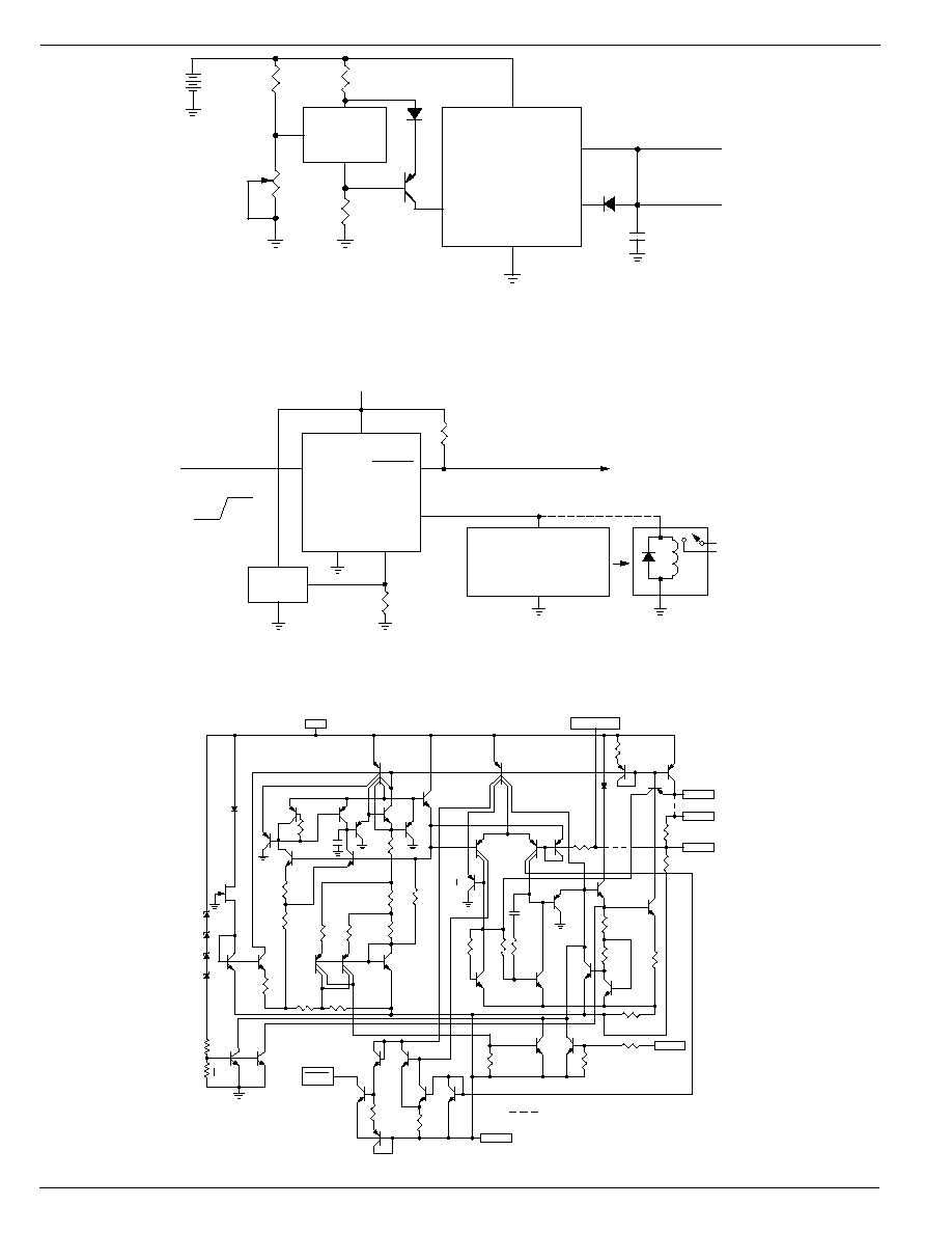
Schematic Diagram
3
MIC2951
SD
V
GND
4
1
8
OUT
+VIN
SENSE
2
+
1µF
LM385
1.5k
**
≠
100k
120k
FB
6V
SEALED
LEAD-
ACID
BATTERY
SOURCE
+
400k
*
FOR 5.5V
AUX. SHUTDOWN
INPUT
3
MIC2951
SD
V
GND
4
5
8
OUT
+VIN
ERROR
1
7
RELAY
EXTERNAL CIRCUIT
PROTECTED FROM
OVER TEMPERATURE
(V+ GOES OFF WHEN
TEMP.> 125
∞
)
OR
10k
5
∞
PRE-SHUTDOWN FLAG
+VIN
LM34 OR
LM35
TEMP.
SENSOR
8.2k
≠
+
FB
OFF
ON
FEEDBACK
SENSE
Q15A
OUT
Q24
Q26
R27
182 k
5V TAP
R28
60 k
R18
20k
Q25
Q23
Q22
R15
100 k
R16
30 k
Q29
Q28
R17
10
R21 8
R17
12 k
Q31
Q30
R23 60 k
SHDN
R24
50 k
R22
150 k
Q21
Q19
C2
40 pF
R14
350
k
Q14
R13
100
k
Q18
R12
110
k
Q20
Q9
Q15B
Q8
Q7
R11
20.6
k
Q5
R8
31.4 k
R10
150
k
R9
27.8 k
Q11
Q12
Q13
R6
140
k
R5
180
k
R4
13 k
R3
50 k
Q2
C1
20
pF
Q4
Q3
R11
18
k
Q6
Q1
10
R1
20 k
R2
50 k
Q41
R30
30
k
Q40
Q34
GND
Q36
Q37
R25
2.8 k
Q38
ERROR
R26
60 k
Q39
DENOTES CONNECTION ON MIC2950 ONLY
Q42
Q16
Q17
50 k
10 k
IN
100 x
MIC2950/2951
Micrel
February 1999
15
MIC2950/2951
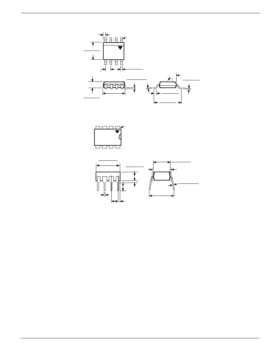
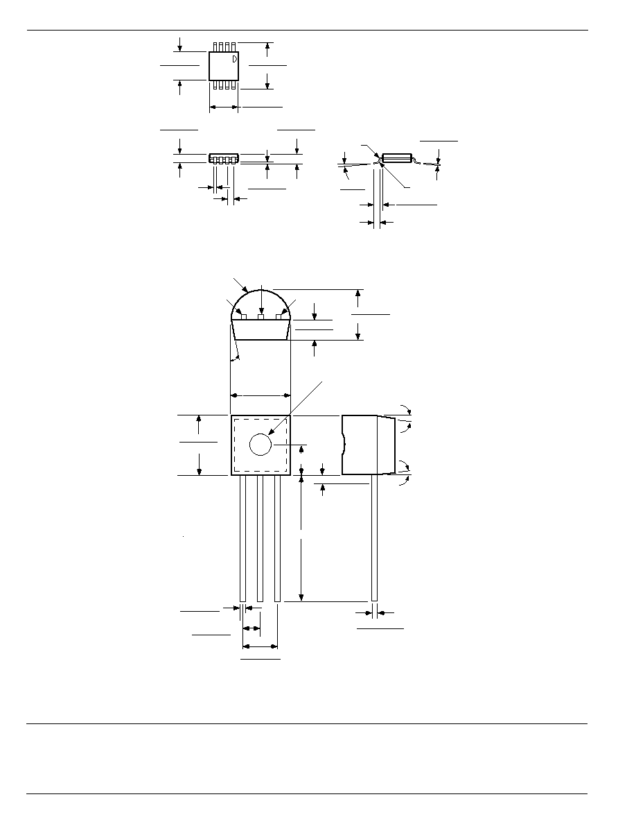
Package Information
45
∞
0
∞
≠8
∞
0.244 (6.20)
0.228 (5.79)
0.197 (5.0)
0.189 (4.8)
SEATING
PLANE
0.026 (0.65)
MAX
)
0.010 (0.25)
0.007 (0.18)
0.064 (1.63)
0.045 (1.14)
0.0098 (0.249)
0.0040 (0.102)
0.020 (0.51)
0.013 (0.33)
0.157 (3.99)
0.150 (3.81)
0.050 (1.27)
TYP
PIN 1
DIMENSIONS:
INCHES (MM)
0.050 (1.27)
0.016 (0.40)
8-Pin SOP (M)
0.380 (9.65)
0.370 (9.40)
0.135 (3.43)
0.125 (3.18)
PIN 1
DIMENSIONS:
INCH (MM)
0.018 (0.57)
0.100 (2.54)
0.013 (0.330)
0.010 (0.254)
0.300 (7.62)
0.255 (6.48)
0.245 (6.22)
0.380 (9.65)
0.320 (8.13)
0.0375 (0.952)
0.130 (3.30)
8-Pin Plastic DIP (N)
MIC2950/2951
Micrel
MIC2950/2951
16
February 1999
0.008 (0.20)
0.004 (0.10)
0.039 (0.99)
0.035 (0.89)
0.021 (0.53)
0.012 (0.03) R
0.0256 (0.65) TYP
0.012 (0.30) R
5
∞
MAX
0
∞
MIN
0.122 (3.10)
0.112 (2.84)
0.120 (3.05)
0.116 (2.95)
0.012 (0.03)
0.007 (0.18)
0.005 (0.13)
0.043 (1.09)
0.038 (0.97)
0.036 (0.90)
0.032 (0.81)
DIMENSIONS:
INCH (MM)
0.199 (5.05)
0.187 (4.74)
8-Lead MSOP (MM)
3
2
1
10
∞
typ.
5
∞
typ.
5
∞
typ.
0.185 (4.699)
0.175 (4.445)
0.185 (4.699)
0.175 (4.445)
0.085 (2.159) Diam.
0.500 (12.70) Min.
0.090 (2.286) typ.
0.0155 (0.3937)
0.0145 (0.3683)
Seating Plane
0.025 (0.635) Max
Uncontrolled
Lead Diameter
0.016 (0.406)
0.014 (0.356)
0.105 (2.667)
0.095 (2.413)
0.055 (1.397)
0.045 (1.143)
0.090 (2.286) Radius, typ.
0.145 (3.683)
0.135 (3.429)
0.055 (1.397)
0.045 (1.143)
BOTTOM VIEW
TO-92 (Z)
MICREL INC.
1849 FORTUNE DRIVE
SAN JOSE, CA 95131
USA
TEL
+ 1 (408) 944-0800
FAX
+ 1 (408) 944-0970
WEB
http://www.micrel.com
This information is believed to be accurate and reliable, however no responsibility is assumed by Micrel for its use nor for any infringement of patents or
other rights of third parties resulting from its use. No license is granted by implication or otherwise under any patent or patent right of Micrel Inc.
© 1999 Micrel Incorporated