
January 2006
1
M9999-010306
MIC3287
Micrel, Inc.
MIC3287
1.2MHz PWM White LED Driver with OVP in
Thin SOT-23 and 2mm x 2mm MFLTM
General Description
The MIC3287 is a 1.2MHz pulse width modulated (PWM)
step-up switching regulator that is optimized for constant
current white LED driving applications. With a maximum
output voltage of 24V and a switch current of over 350mA,
the MIC3287 drives a string of up to 4 white LEDs in series,
ensuring uniform brightness and eliminating several ballast
resistors.
The MIC3287 implements a constant frequency 1.2MHz PWM
current-mode control scheme. The high frequency PWM op-
eration saves board space by reducing external component
sizes. The added benefit of the constant frequency PWM
control scheme as opposed to variable frequency control
schemes is much lower noise and input ripple injected back
to the battery source. To optimize efficiency, the feedback
voltage is set to only 250mV. The MIC3287 is also available
with a maximum 24V over-voltage protection.
The MIC3287 is available in low profile Thin SOT-23 5-pin
and Thin SOT-23 6-pin packages. The MIC3287 has a junc-
tion temperature range of �40�C to +125�C.
All support documentation can be found on Micrel's web site
at: www.micrel.com.
Typical Application
10�H
0.22�F
250mV
1-Cell
Li Ion
1�F
2
3
1
4
5
MIC3287YD5
VIN
EN
SW
FB
GND
3-Series White LED Driver in Thin SOT-23-5
Features
� 2.8V to 5.5V Input Voltage
� 350mA Switch Current
� 1.2 MHz PWM Operation
� 250mV Feedback Voltage
� 24V Output Over-Voltage Protection (OVP) Option
� <1% Line and Load Regulation
� <1�A Shutdown Current
� Over-Temperature Protection
� Under-Voltage Lock Out (UVLO)
� Low Profile Thin SOT-23-5 Package Option
� Low Profile Thin SOT-23-6 Package Option
� 8-pin 2mm x 2mm MLFTM Package Option
� �40�C to +125�C Junction Temperature Range
Applications
� White LED Driver for Backlighting:
- Cell phones
- PDAs
- GPS systems
- Digital cameras
- MP3 players
- IP phones
� LED Flashlights
� Constant Current Power Supplies
Micrel, Inc. � 2180 Fortune Drive � San Jose, CA 95131 � USA � tel + 1 (408) 944-0800 � fax + 1 (408) 474-1000 � http://www.micrel.com
MLF and MicroLeadFrame are trademarks of Amkor Technology, Inc.
10�H
0.22�F
1�F
1-Cell
Li Ion
MIC3287-24YD6
VIN
EN
SW
OVP
FB
GND
250mV
5
1
3
4
4
6
4-Series White LED Driver
with Output OVP in Thin SOT-23-6
MIC3287
Micrel, Inc.
M9999-010306
2
January 2006
Pin Configuration
FB GND
EN
VIN
SW
3
1
5
2
4
FB GND
EN
VIN
SW
3
1
6
2
4
5
OVP
TSOT-23-5 (YD5)
TSOT-23-6 (YD6)
1
VIN
OVP
EN
AGND
8 PGND
SW
NC
FB
7
6
5
2
3
4
EP
8-Pin 2mm x 2mm MLFTM (YML)
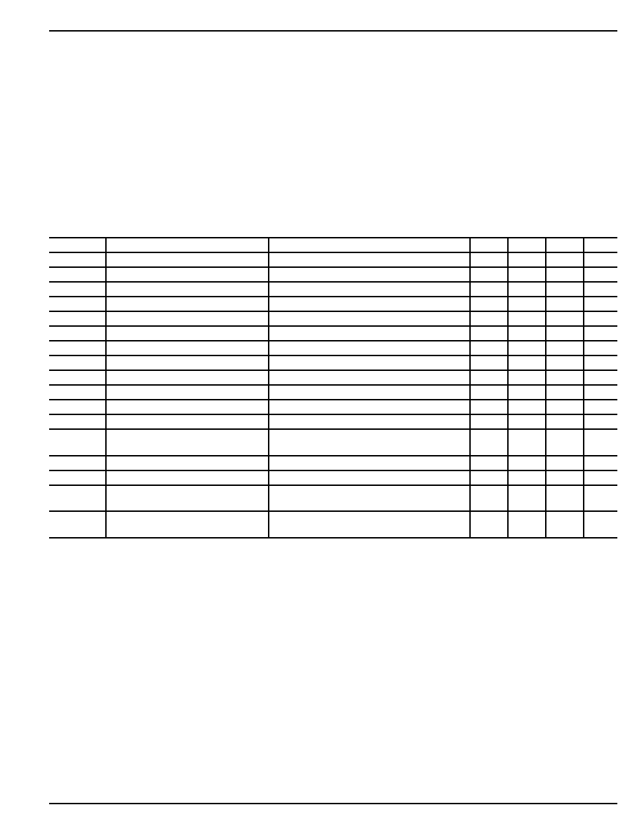
Ordering Information
Part Number
Marking
Code
Overvoltage
Protection
Junction
Temp. Range
Package
Lead Finish
MIC3287YD5
WGAA
N/A
-40�C to +125�C
Thin SOT-23-5
Lead Free
MIC3287-24YD6
WHAA
24V
-40�C to +125�C
Thin SOT-23-6
Lead Free
MIC3287-24YML
WLA
24V
-40�C to +125�C
8-Pin 2mm x 2mm MLF
Lead Free
Ordering Information
Pin Number
TSOT-23-5
Pin Number
TSOT-23-6
Pin Number
8-Pin MLF
Pin Name
Pin Function
1
1
7
SW
Switch Node (Input): Internal power bipolar collector.
2
2
4
AGND
Analog Ground (Return): Ground.
2
2
8
PGND
Power Ground (Return): Ground.
3
3
5
FB
Feedback (Input): Output voltage sense node. Connect the cathode of the
LED to this pin. A resistor from this pin to ground sets the LED current.
4
4
3
EN
Enable (Input): Logic high enables regulator. Logic low shuts down regu-
lator.
5
6
1
VIN
Supply (Input): 2.8V to 5.5V for internal circuitry.
--
5
2
OVP
Overvoltage Protection (Input): Connect to the output.
--
--
6
NC
Not Connected
--
--
EP
EP
Exposed Backside Pad: Connect to ground.
January 2006
3
M9999-010306
MIC3287
Micrel, Inc.
Absolute Maximum Ratings
(1)
Supply Voltage (V
IN
) ........................................................ 6V
Switch Voltage (V
SW
) ......................................�0.3V to 34V
Enable Pin Voltage (V
EN
) ................................... �0.3 to V
IN
FB Voltage (V
FB
) ............................................................. 6V
Switch Current (I
SW
) ..................................................... 1.2A
Ambient Storage Temperature (T
S
) .......... �65�C to +150�C
ESD Rating
(3)
................................................................ 2kV
Operating Ratings
(2)
Supply Voltage (V
IN
) .........................................2.8V to 5.5V
Output Voltage (V
OUT
)
(4)
...................................V
IN
to V
OUT
Junction Temperature Range (T
J
) ............ �40�C to +125�C
Package Thermal Impedance
Thin SOT-23-5 (
JA
)
(5)
.......................................207�C/W
Thin SOT-23-6 (
JA
)
(5)
.......................................134�C/W
8-Pin MLF (
JA
) ...................................................90�C/W
Electrical Characteristics
(6)
T
A
= 25�C, V
IN
= V
EN
= 3.6V, V
OUT
= 10V, I
OUT
= 10mA, unless otherwise noted.
Bold values indicate �40�C T
J
125�C.
Symbol
Parameter
Condition
Min
Typ
Max
Units
V
IN
Supply Voltage Range
2.8
5.5
V
V
UVLO
Under Voltage Lockout
1.8
2.1
2.4
V
I
VIN
Quiescent Current
V
FB
> 500mV, (not switching)
2.1
5
mA
I
SD
Shutdown Current
V
EN
= 0V
(7)
0.04
1
�A
V
FB
Feedback Voltage
(�7.5%)
231
250
269
mV
I
FB
Feedback Input Current
V
FB
= 250mV
�450
nA
Line Regulation
3V V
IN
5V
(8)
0.4
1
%
Load Regulation
5mA I
OUT
20mA
(8)
0.5
%
D
MAX
Maximum Duty Cycle
85
90
%
I
SW
Switch Current Limit
V
IN
= 3.6V
350
mA
V
SW
Switch Saturation Voltage
V
IN
= 3.6V, I
SW
= 300mA
250
mV
I
SW
Switch Leakage Current
V
EN
= 0V, V
SW
= 10V
0.01
1
�A
V
EN
Enable Threshold
TURN ON
1.5
V
TURN OFF
0.4
V
I
EN
Enable Pin Current
V
EN
= 10V
21
40
�A
f
SW
Oscillator Frequency
1
1.2
1.4
MHz
V
OVP
Overvoltage Protection
MIC3287 - 24YD6
17
19
24
V
MIC3287-24YML
T
J
Overtemperature
150
�C
Threshold Shutdown
Hysteresis
10
�C
Notes:
1. Absolute maximum ratings indicate limits beyond which damage to the component may occur. Electrical specifications do not apply when operating
the device outside of its operating ratings. The maximum allowable power dissipation is a function of the maximum junction temperature, T
J
(max),
the junction-to-ambient thermal resistance,
JA
, and the ambient temperature, T
A
. The maximum allowable power dissipation will result in excessive
die temperature, and the regulator will go into thermal shutdown.
2. This device is not guaranteed to operate beyond its specified operating ratings.
3. Devices are inherently ESD sensitive. Handling precautions required. Human body model.
4. For options with OVP.
5. Using 4 layer PCB.
6. Specification for packaged product only.
7. I
SD
= I
VIN
.
8. Guaranteed by design.
MIC3287
Micrel, Inc.
M9999-010306
4
January 2006
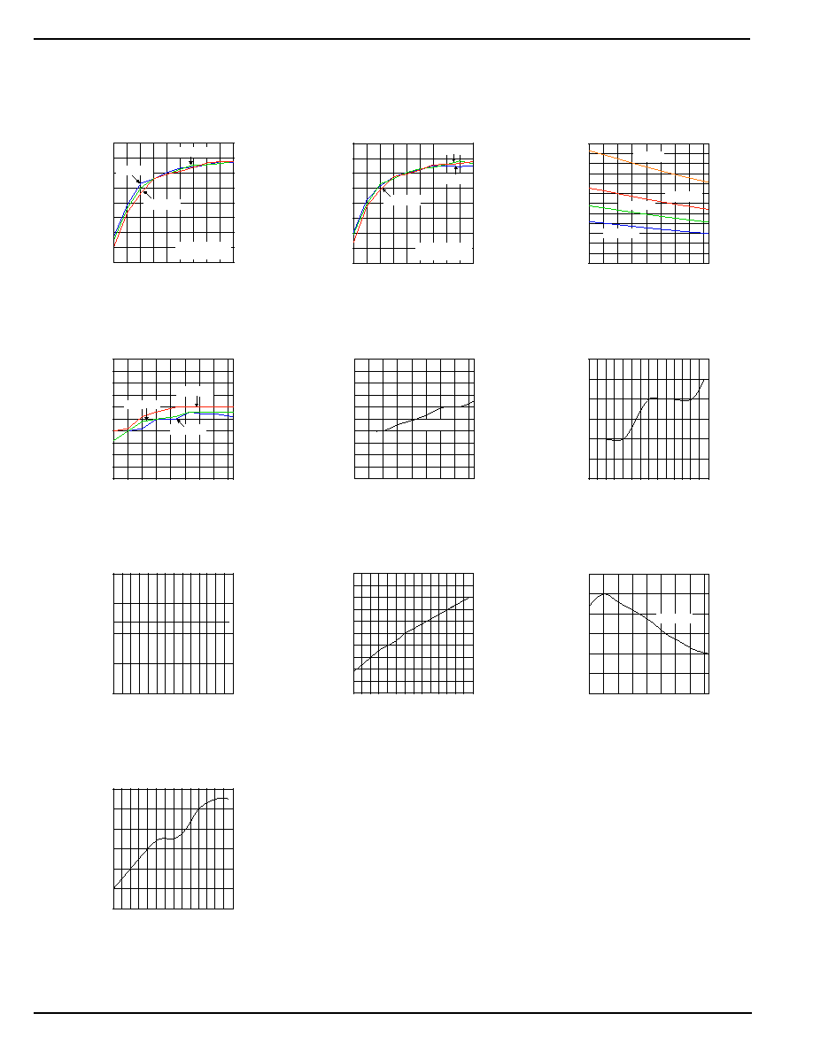
Typical Characteristics
45
50
55
60
65
70
75
80
85
2 4 6 8 10 12 14 16 18 20
EFFICIENCY (%
)
WHITE LED CURRENT (mA)
3 Series
White LED Efficiency
V
IN
=3.2V
V
IN
=3.6V
V
IN
=4.2V
L = 10�H
C
OUT
= 0.22�F
45
50
55
60
65
70
75
80
85
2 4 6 8 10 12 14 16 18 20
EFFICIENCY (%
)
WHITE LED CURRENT (mA)
4 Series
White LED Efficiency
V
IN
=3.2V
V
IN
=3.6V
V
IN
=4.2V
L = 10�H
C
OUT
= 0.22�F
0
2
4
6
8
10
12
-40
ENABLE PIN CURRENT (�A)
TEMPERATURE (�C)
Enable Pin Current
vs. Temperature
-25 -10 5 20 35 50 65 80
V
EN
=1.8V
V
EN
=2.5V
V
EN
=3.3V
V
EN
=5V
1.0
1.1
1.2
1.3
1.4
1.5
FREQUENCY (MHz)
Frequency
vs. Temperature
-40
TEMPERATURE (�C)
-25 -10 5 20 35 50 65 80
V
IN
=3.2V
V
IN
=3.6V
V
IN
=4.2V
240
244
248
252
256
260
FEEDBACK VOLTAGE (mV)
Feedback Voltage
vs. Temperature
-40
TEMPERATURE (�C)
-25 -10 5 20 35 50 65 80
V
IN
=3.6V
248
249
250
251
252
253
254
2.8
FEEDBACK VOLTAGE (mV)
INPUT VOLTAGE (V)
Feedback Voltage
vs. Input Voltage
3.2 3.6 4.0 4.4 4.8 5.2 5.6
2.0
2.1
2.2
2.3
2.4
2.5
2.8
QUIESCENT CURRENT (mA)
Quiescent Current
vs. Input Voltage
INPUT VOLTAGE (V)
3.2 3.6 4.0 4.4 4.8 5.2 5.6
600
650
700
750
800
850
900
CURRENT LIMIT (mA)
Curremt Limit
vs. Temperature
-40
TEMPERATURE (�C)
-25 -10 5 20 35 50 65 80
V
IN
=3.6V
720
740
760
780
800
820
840
2.8
CURRENT LIMIT (mA)
Current Limit
vs. Input Voltage
INPUT VOLTAGE (V)
3.2 3.6 4.0 4.4 4.8 5.2 5.6
0.001
0.002
0.003
2.8
SHUTDOWN CURRENT (uA)
Shutdown Current
vs. Input Voltage
INPUT VOLTAGE (V)
3.2 3.6 4.0 4.4 4.8 5.2 5.6
January 2006
5
M9999-010306
MIC3287
Micrel, Inc.
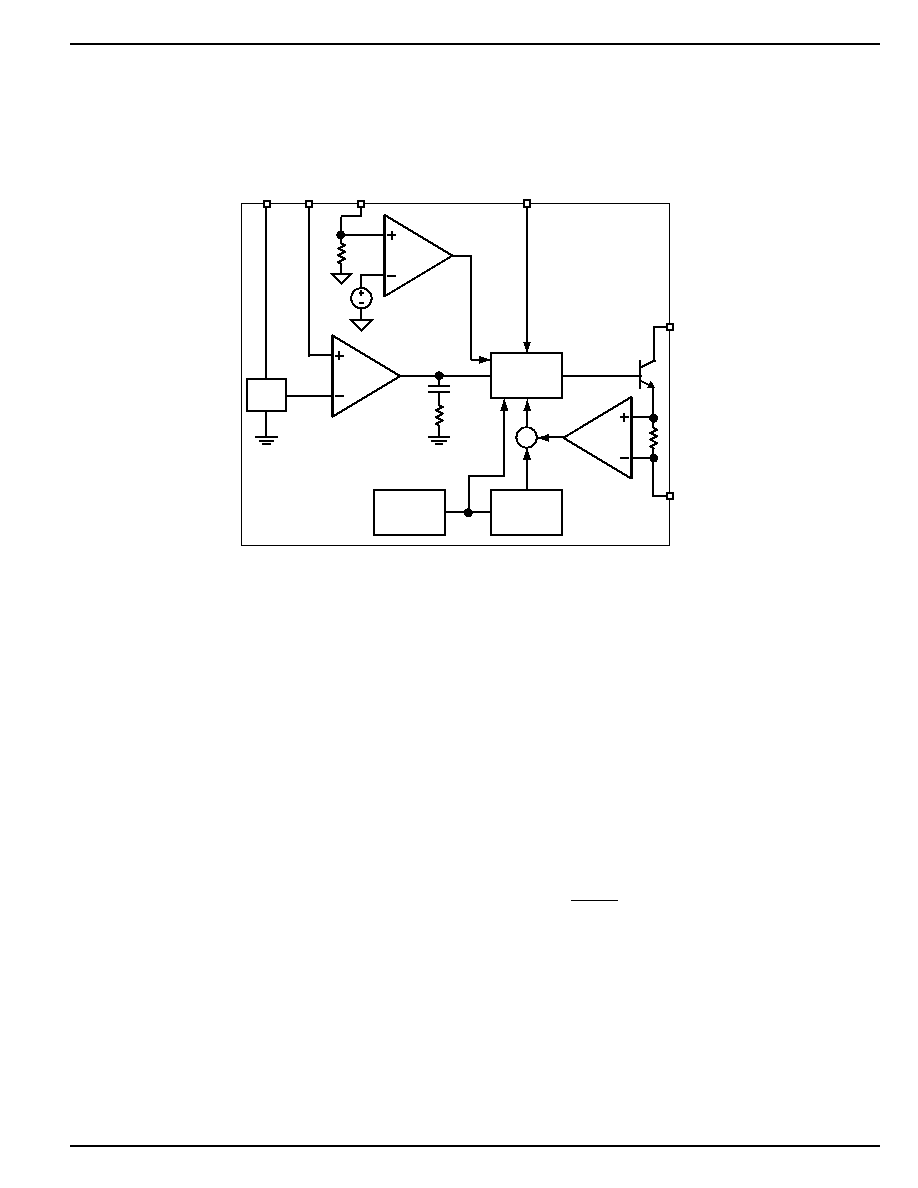
Functional Description
The MIC3287 is a constant frequency pulse width modulated
(PWM) current-mode step-up regulator. The block diagram
is shown above. The MIC3287 is composed of an oscillator,
slope compensation ramp generator, current amplifier, g
m
er-
ror amplifier, PWM generator, and a 350mA minimum bipolar
output transistor. The oscillator generates a 1.2MHz clock.
The clock's two functions are to trigger the PWM generator
that turns on the output transistor and to reset the slope com-
pensation ramp generator. The current amplifier is used to
measure the switch current by amplifying the voltage signal
from the internal sense resistor. The output of the current
amplifier is summed with the output of the slope compensa-
tion ramp generator. This summed current-loop signal is fed
to one of the inputs of the PWM generator.
Functional Diagram
GND
V
REF
PWM
Generator
Ramp
Generator
1.2MHz
Oscillator
SW
EN
FB
OVP*
VIN
250mV
g
m
OVP
V
REF
Error
Amplifier
Current
Amplifier
* OVP available on TSOP-23-6 and MLFTM package options only.
MIC3287 Block Diagram
The g
m
error amplifier measures the LED current through the
external sense resistor and amplifies the error between the
detected signal and the internal 250mV reference voltage.
The output of the g
m
error amplifier provides the voltage-loop
signal that is fed to the other input of the PWM generator.
When the current-loop signal exceeds the voltage-loop signal,
the PWM generator turns off the bipolar output transistor. The
next clock period initiates the next switching cycle, thus main-
taining the constant frequency current-mode PWM control.
The LED current is set by the feedback resistor:
I
LED
=
250mV
R
FB
The enable pin shuts down the internal power bipolar
transistor and disables the control circuitry to reduce input
current-to-leakage levels. Enable pin input current is zero
at zero volts.