
August 2003
1
MIC37150/37151/37152
MIC37150/37151/37152
Micrel
MIC37150/37151/37152
1.5A, Low Voltage
µ
Cap LDO Regulator
General Description
The Micrel MIC37150/51/52 is a 1.5A low-dropout linear
voltage regulator that provides a low voltage, high current
output with a minimum of external components. It offers high
precision, ultra-low dropout (500mV over temperature), and
low ground current.
The MIC37150/51/52 operates from an input of 2.25V to
6.0V. It is designed to drive digital circuits requiring low
voltage at high currents (i.e., PLDs, DSPs, microcontrollers,
etc.). It is available in fixed and adjustable output voltages.
Fixed voltages include 1.5V, 1.65V, 1.8V, 2.5V and 3.3V. The
adjustable version is capable of supplying output voltages
from 1.24V to 5.5V.
Features of the MIC37150/51/52 LDO include thermal and
current limit protection, and reverse current and reverse
battery protection. Logic enable and error flag pins are
available.
Junction temperature range of the MIC37150/51/52 is from
≠40
∞
C to 125
∞
C.
For applications requiring input voltage greater than 6.0V,
see MIC3910x, MIC3915x, MIC3930x, and MIC3950x LDOs.
Data sheets and support documentation can be found on
Micrel's web site at www.micrel.com.
Typical Application
VOUT
VIN
FLG
GND
VEN
C
OUT
47µF, Ceramic
100k
MIC37151
V
IN
= 3.0V
V
OUT
= 2.5V
C
IN
Fixed 2.5V Regulator with Error Flag
VOUT
VIN
ADJ
GND
VEN
C
OUT
47µF, Ceramic
R1
R2
1.3V
MIC37152
V
IN
C
IN
Adjustable Regulator
Features
∑ 1.5A minimum guaranteed output current
∑ 500mV maximum dropout voltage over temperature
Ideal for 3.0V to 2.5V conversion
Ideal for 2.5V to 1.8V, 1.65V, or 1.5V conversion
∑ Stable with ceramic or tantalum capacitor
∑ Wide input voltage range:
V
IN
: 2.25V to 6.0V
∑ +1.0% initial output tolerance
∑ Fixed and adjustable output voltages
MIC37150--3-pin fixed voltages
MIC37151--5-pin fixed voltages
MIC37152--5-pin adjustable voltage
∑ Excellent line and load regulation specifications
∑ Logic controlled shutdown
∑ Thermal shutdown and current limit protection
∑ Reverse-leakage protection
∑ Low profile S-Pak 3 or 5 pin packages
Applications
∑ LDO linear regulator for low-voltage digital IC
∑ PC add-in cards
∑ High efficiency linear power supplies
∑ SMPS post regulator
∑ Battery charger
Micrel, Inc. ∑ 1849 Fortune Drive ∑ San Jose, CA 95131 ∑ USA ∑ tel + 1 (408) 944-0800 ∑ fax + 1 (408) 944-0970 ∑ http://www.micrel.com
Super þeta PNP is a trademark of Micrel, Inc.
MIC37150/37151/37152
Micrel
MIC37150/37151/37152
2
August 2003
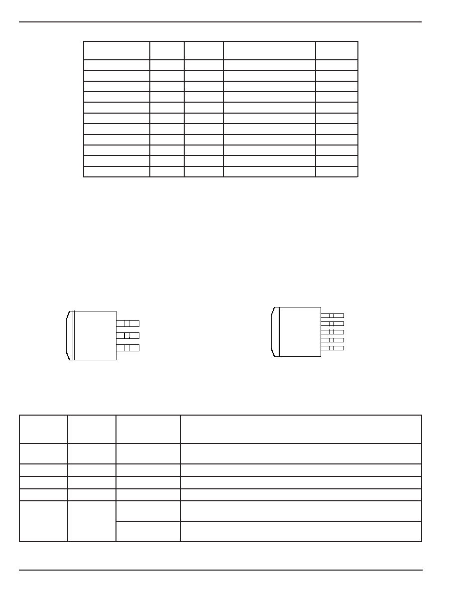
Ordering Information
Output
Part Number
Current
Voltage*
Junction Temp. Range
Package
MIC37150-1.5BR
1.5A
1.5V
≠40
∞
C to +125
∞
C
S-Pak-3
MIC37150-1.65BR
1.5A
1.65V
≠40
∞
C to +125
∞
C
S-Pak-3
MIC37150-1.8BR
1.5A
1.8V
≠40
∞
C to +125
∞
C
S-Pak-3
MIC37150-2.5BR
1.5A
2.5V
≠40
∞
C to +125
∞
C
S-Pak-3
MIC37150-3.3BR
1.5A
3.3V
≠40
∞
C to +125
∞
C
S-Pak-3
MIC37151-1.5BR
1.5A
1.5V
≠40
∞
C to +125
∞
C
S-Pak-5
MIC37151-1.65BR
1.5A
1.65V
≠40
∞
C to +125
∞
C
S-Pak-5
MIC37151-1.8BR
1.5A
1.8V
≠40
∞
C to +125
∞
C
S-Pak-5
MIC37151-2.5BR
1.5A
2.5V
≠40
∞
C to +125
∞
C
S-Pak-5
MIC37151-3.3BR
1.5A
3.3V
≠40
∞
C to +125
∞
C
S-Pak-5
MIC37152BR
1.5A
ADJ.
≠40
∞
C to +125
∞
C
S-Pak-5
*For other voltages contact Micrel.
Pin Configuration
TA
B
3
OUT
2
GND
1
IN
S-PAK-3 (R)
MIC37150
TA
B
5
FLG/ADJ
4
VOUT
3
GND
2
VIN
1
EN
S-PAK-5 (R)
MIC37151
MIC37152
Pin Description
Pin Number
Pin Number
Pin Name
Pin Function
MIC37150
MIC37151/2
S-PAK-3
S-PAK-5
≠
1
EN
Enable (Input): CMOS compatible input. Logic high = enable, logic
low = shutdown.
1
2
VIN
Input voltage which supplies current to the output power device.
2
3
GND
Ground (TAB is connected to ground on S-Pak)
3
4
VOUT
Regulator Output
≠
5
FLG
Error Flag (Output): Open collector output. Active low indicates an output
MIC37151 only
fault condition.
ADJ
Adjustable regulator feedback input. Connect to resistor voltage divider.
MIC37152 only
August 2003
3
MIC37150/37151/37152
MIC37150/37151/37152
Micrel
Electrical Characteristics
(Note 5)
T
A
= 25
∞
C with V
IN
= V
OUT
+ 1V; V
EN
= V
IN
; bold values indicate ≠40
∞
C < T
J
< +125
∞
C; unless otherwise noted.
Parameter
Condition
Min
Typ
Max
Units
Output Voltage Accuracy
I
L
= 10mA
≠1
+1
%
10mA < I
OUT
< I
L(max)
, V
OUT
+ 1
V
IN
6V
≠2
+2
%
Output Voltage Line Regulation
V
IN
= V
OUT
+1.0V to 6.0V
0.06
0.5
%
Output Voltage Load Regulation
I
L
= 10mA to 1.5A
0.2
1
%
V
IN
≠ V
OUT
; Dropout Voltage;
I
L
= 750mA
350
mV
Note 6
I
L
= 1.5A
500
mV
Ground Pin Current, Note 7
I
L
= 1.5A
17
30
mA
Ground Pin Current in Shutdown
V
IL
0.5V, V
IN
= V
OUT
+ 1V
1.0
µ
A
Current Limit
V
OUT
= 0
2.25
4.0
A
Start-up Time
V
EN
= V
IN
, I
OUT
= 10mA, C
OUT
= 22
µ
F
170
500
µ
s
Enable Input
Enable Input Threshold
Regulator enable
2.25
V
Regulator shutdown
0.8
V
Enable Pin Input Current
V
IL
0.8V (regulator shutdown)
2
µ
A
4
µ
A
V
IH
2.25V (regulator enabled)
1
15
30
µ
A
75
µ
A
Flag Output
I
FLG(LEAK)
V
OH
= 6V
1
µ
A
2
µ
A
V
FLG(LO)
V
IN
= 2.25V, I
OL
= 250
µ
A, Note 8
210
300
mV
400
mV
V
FLG
Low threshold, % of V
OUT
below nominal
93
%
Hysteresis
2
%
High threshold, % of V
OUT
below nominal
99.2
%
Reference Voltage
1.228
1.240
1.252
V
Reference Voltage
Note 9
1.215
1.265
V
Adjust Pin Bias Current
40
80
nA
120
nA
Reference Voltage
Note 10
20
ppm/
∞
C
Temp. Coefficient
Adjust Pin Bias Current
0.1
nA/
∞
C
Temp. Coefficient
Absolute Maximum Rating
(Note 1)
Supply Voltage (V
IN
) .................................................... 6.5V
Enable Input Voltage (V
EN
) .......................................... 6.5V
Power Dissipation .................................... Internally Limited
Junction Temperature ........................ ≠40
∞
C
T
J
+125
∞
C
Storage Temperature ......................... ≠65
∞
C
T
J
+150
∞
C
Lead Temperature (soldering, 5 sec.) ....................... 260
∞
C
ESD, Note 3
Operating Maximum Rating
(Note 2)
Supply Voltage (V
IN
) ..................................... 2.25V to 6.0V
Enable Input Voltage (V
EN
) ................................ 0V to 6.0V
Junction Temperature Range ............. ≠40
∞
C
T
J
+125
∞
C
Maximum Power Dissipation .................................... Note 4
Package Thermal Resistance
S-Pak(
JC
) ......................................................... 2
∞
C/W

MIC37150/37151/37152
Micrel
MIC37150/37151/37152
4
August 2003
Note 1.
Exceeding the absolute maximum ratings may damage the device.
Note 2.
The device is not guaranteed to function outside its operating rating.
Note 3.
Device is ESD sensitive. Handling precautions recommended.
Note 4.
P
D(MAX)
= (T
J(MAX)
≠ T
A
) /
JA
, where
JA
, depends upon the printed circuit layout. See
"Applications Information."
Note 5.
Specification for packaged product only.
Note 6.
V
DO
= V
IN
≠ V
OUT
when V
OUT
decreased to 98% of its nominal output voltage with V
IN
= V
OUT
+1V. For output voltages below 1.75V, dropout
voltage specification does not apply due to a minimum input operating voltage of 2.25V.
Note 7.
I
GND
is the quiescent current. I
IN
= I
GND
+ I
OUT
.
Note 8.
For a 2.5V device, V
IN
= 2.250V (device is in dropout).
Note 9.
V
REF
V
OUT
(V
IN
≠1.0V), 2.25V
V
IN
6.0V, 10mA
I
L
1.5A, T
J
= T
MAX
.
Note 10. Thermal regulation is defined as the change in output voltage at a time t after a change in power dissipation is applied, excluding load or line
regulation effects. Specifications are for a 200mA load pulse at V
IN
= 6V for t = 10ms.
August 2003
5
MIC37150/37151/37152
MIC37150/37151/37152
Micrel
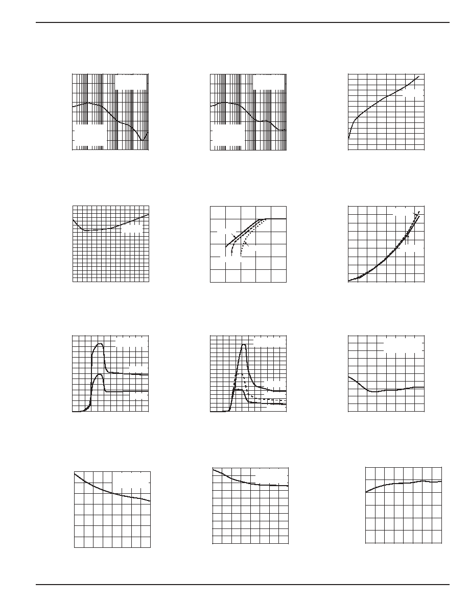
Typical Characteristics
0
20
40
60
80
1E-2 1E-1 1E+0 1E+1 1E+2 1E+3
PSRR (dB)
FREQUENCY (Hz)
Power Supply
Rejection Ratio
I
OUT
= 1.5A
C
OUT
= 10
µ
F
C
IN
= 0
V
IN
= 3.3V
V
OUT
= 2.5V
0.01 0.1
1
10
100
1k
0
20
40
60
80
1E-2 1E-1 1E+0 1E+1 1E+2 1E+3
PSRR (dB)
FREQUENCY (Hz)
Power Supply
Rejection Ratio
I
OUT
= 1.5A
C
OUT
= 47
µ
F
C
IN
= 0
V
IN
= 3.3V
V
OUT
= 2.5V
0.01 0.1
1
10
100
1k
0
50
100
150
200
250
300
350
0
400
800
1200
1600
DROPOUT VOLTAGE (mV)
OUTPUT CURRENT (mA)
Dropout Voltage vs.
Output Current
2.5V
OUT
0
50
100
150
200
250
300
350
400
450
500
-40 -20 0
20 40 60 80 100 120
DROPOUT VOLTAGE (mV)
TEMPERATURE (
∞
C)
Dropout Voltage vs.
Temperature
2.5V
OUT
0
0.5
1.0
1.5
2.0
2.5
3.0
1
1.5
2
2.5
3
3.5
OUTPUT VOLTAGE (V)
INPUT VOLTAGE (V)
Dropout Characteristics
100mA
750mA
1.5A
0
2
4
6
8
10
12
14
16
18
0
200
400
600
800
1000
1200
1400
1600
GROUND CURRENT (mA)
OUTPUT CURRENT (mA)
Ground Current
vs. Output Current
1.5V
OUT
2.5V
OUT
0
0.2
0.4
0.6
0.8
1
1.2
1.4
0
1
2
3
4
5
6
GROUND CURRENT (mA)
SUPPLY VOLTAGE (V)
Ground Current
vs. Supply Voltage
V
OUT
= 2.5V
10mA
100mA
0
5
10
15
20
25
30
35
40
45
0
1
2
3
4
5
6
GROUND CURRENT (mA)
SUPPLY VOLTAGE (V)
Ground Current
vs. Supply Voltage
V
OUT
= 2.5V
1500mA
750mA
1000mA
0.4
0.405
0.41
0.415
0.42
0.4
0.43
0.435
0.44
0.445
0.5
-40 -20 0
20 40 60 80 100 120
GROUND CURRENT (mA)
TEMPERATURE (
∞
C)
Ground Current
vs. Temperature
V
OUT
= 2.5V
I
LOAD
= 10mA
0
2
4
6
8
10
12
14
16
18
20
-40 -20 0
20 40 60 80 100 120
GROUND CURRENT (mA)
TEMPERATURE (
∞
C)
Ground Current
vs. Temperature
V
OUT
=2.5V
I
LOAD
= 1.5A
0
0.5
1.0
1.5
2.0
2.5
3.0
-40 -20 0
20 40 60 80 100 120
SHORT CIRCUIT CURRENT (mA)
TEMPERATURE (
∞
C)
Short Circuit Current
vs. Temperature
0
1
2
3
4
5.0
6
7
-40 -20 0
20 40 60 80 100 120
GROUND CURRENT (mA)
TEMPERATURE (
∞
C)
Ground Current
vs. Temperature
V
OUT
= 2.5V
I
LOAD
= 750mA