January 2003
1
MIC37252
MIC37252
Micrel
MIC37252
2.5A, Low Voltage
µ
Cap LDO Regulator
Final
General Description
The Micrel MIC37252 is a 2.5A low-dropout linear voltage
regulator that provides a low voltage, high current output with
a minimum of external components. It offers high precision,
low dropout and low ground current.
The MIC37252 operates from an input voltage of 3.0V to
6.0V. It is designed to drive digital circuits requiring low
voltage at high currents (i.e., PLDs, DSP, microcontroller,
etc.). It is available in an adjustable output voltage capable of
1.24V to 5.5V.
Features of the MIC37252 LDO include thermal and current
limit protection, and reverse current and reverse battery
protection.
Junction temperature range of the MIC37252 is from ≠40
∞
C
to 125
∞
C.
For higher currents see the MIC3730x family of LDOs.
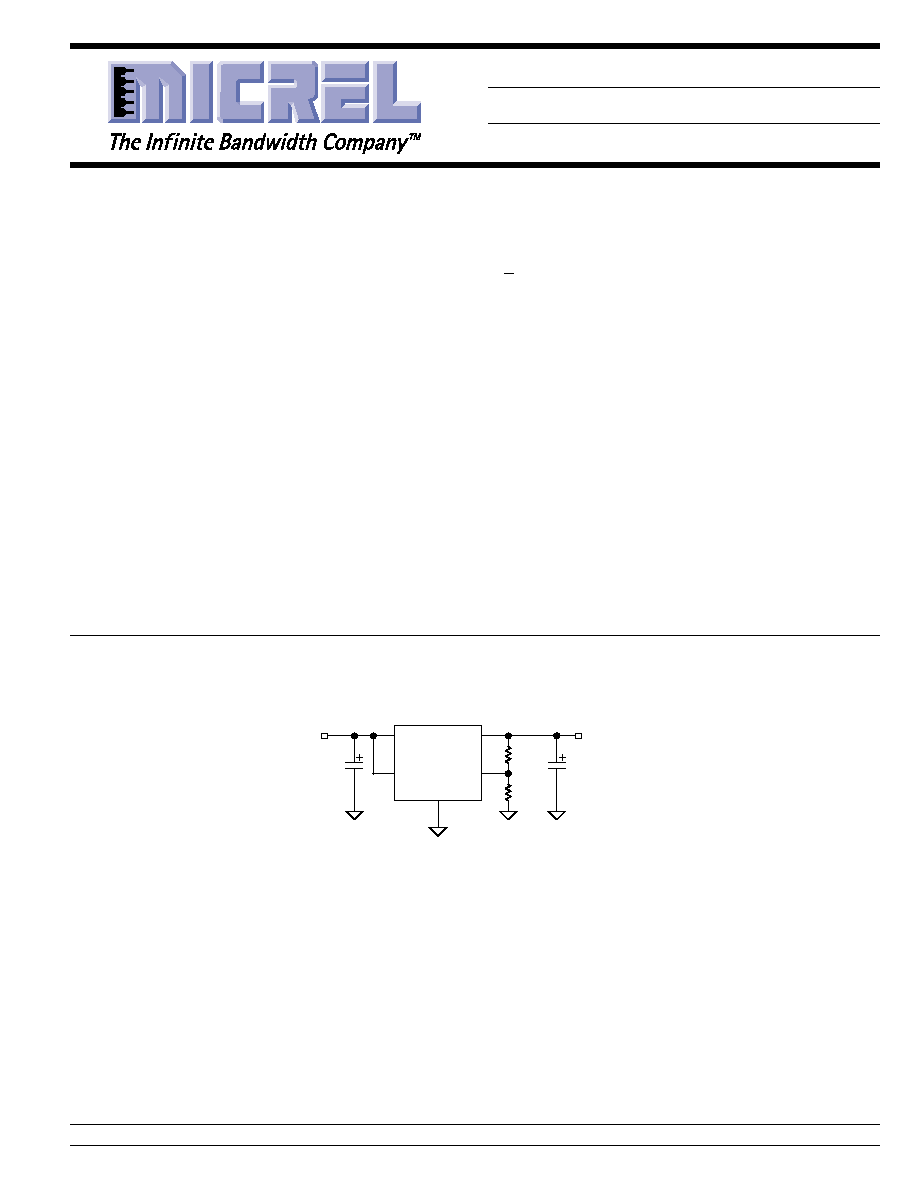
Typical Application
VOUT
VIN
ADJ
GND
VEN
C
OUT
47
µ
F, Ceramic
R1
R2
1.8V
MIC37252
3.3V
C
IN
Adjustable Regulator
Features
∑ 2.5A minimum guaranteed output current
∑ Ideal for 3.3V to 1.8V conversion
∑ Stable with ceramic or tantalum capacitor
∑ +2.0% initial output tolerance
∑ Dropout voltage = 550mV @ 2.5A
∑ Excellent line and load regulation specifications
∑ Logic controlled shutdown
∑ Thermal shutdown and current limit protection
∑ Reverse-leakage protection
∑ S-Pak and TO-263 packages
Applications
∑ LDO linear regulator for low-voltage digital IC
∑ PC add-in cards
∑ High efficiency linear power supplies
∑ SMPS post regulator
∑ Battery charger
Micrel, Inc. ∑ 1849 Fortune Drive ∑ San Jose, CA 95131 ∑ USA ∑ tel + 1 (408) 944-0800 ∑ fax + 1 (408) 944-0970 ∑ http://www.micrel.com
SuperSwitcher and Super
eta PNP are trademarks of Micrel, Inc.
MIC37252
Micrel
MIC37252
2
January 2003
Ordering Information
Output
Part Number
Current
Voltage*
Junction Temp. Range
Package
MIC37252BR
2.5A
ADJ.
≠40
∞
C to +125
∞
C
S-Pak
MIC37252BU
2.5A
ADJ.
≠40
∞
C to +125
∞
C
TO-263-5
*For other voltages contact Micrel.
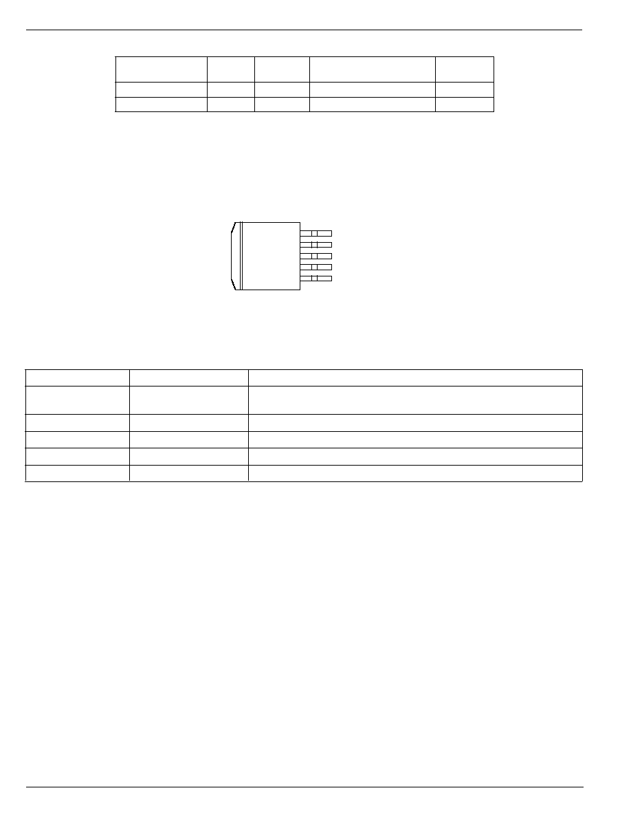
Pin Configuration
TA
B
5
ADJ
4
VOUT
3
GND
2
VIN
1
EN
S-PAK5 (R)
TO-263 (U)
Pin Description
Pin Number
Pin Name
Pin Function
1
EN
Enable (Input): CMOS compatible input. Logic high = enable, logic
low = shutdown
2
VIN
Input voltage which supplies current to the output power device.
3
GND
Ground (TAB is connected to ground on S-Pak)
4
VOUT
Regulator Output
5
ADJ
Adjustable regulator feedback input. Connect to resistor voltage divider.
January 2003
3
MIC37252
MIC37252
Micrel
Electrical Characteristics
T
A
= 25
∞
C with V
IN
= V
OUT
+ 1V; V
EN
= V
IN
; I
L
= 10mA; bold values indicate ≠40
∞
C < T
J
< +125
∞
C; unless otherwise noted.
Parameter
Condition
Min
Typ
Max
Units
Output Voltage Accuracy
I
L
= 10mA
≠2
+2
%
10mA < I
OUT
< I
L(max)
, V
OUT
+ 1
V
IN
6V
≠3
+3
%
Output Voltage Line Regulation
V
IN
= V
OUT
+1.0V to 6.0V, I
L
= 10mA
0.02
0.5
%
Output Voltage Load Regulation
I
L
= 10mA to 2.5A
0.2
1
%
V
IN
≠ V
OUT
; Dropout Voltage ;
I
L
= 1.5A
400
500
mV
Note 5
I
L
= 2.5A
550
1000
mV
Ground Pin Current, Note 6
I
L
= 2.5A
40
60
mA
Ground Pin Current in Shutdown
V
IL
< 0.5V, V
IN
= V
OUT
+ 1V
1.0
µ
A
Current Limit
V
OUT
= 0; V
IN
= 3.3V
3
A
Start-up Time
V
EN
= V
IN
, I
OUT
= 10mA, C
OUT
= 47
µ
F
150
250
µ
s
Enable Input
Enable Input Threshold
Regulator enable
2.25
V
Regulator shutdown
0.8
V
Enable Pin Input Current
V
IL
< 0.8V (Regulator shutdown)
2
µ
A
4
µ
A
V
IH
> 2.25V (Regulator enabled)
1
10
30
µ
A
Reference Voltage
1.215
1.240
1.265
V
1.202
1.277
V
Adjust Pin Bias Current
40
80
nA
120
nA
Note 1.
Exceeding the absolute maximum ratings may damage the device.
Note 2.
The device is not guaranteed to function outside its operating rating.
Note 3.
Device is ESD sensitive. Handling precautions recommended.
Note 4.
P
D(MAX)
= (T
J(MAX)
≠ T
A
) /
JA
, where
JA
, depends upon the printed circuit layout. See "Applications Information."
Note 5.
V
DO
= V
IN
≠ V
OUT
when V
OUT
decreased to 98% of its nominal output voltage with V
IN
= V
OUT
+1V. For output voltages below 2V, dropout
voltage specification does not apply due to a minimum input operating voltage of 3V.
Note 6.
I
GND
is the quiescent current. I
IN
= I
GND
+ I
OUT
.
Absolute Maximum Rating (Note 1)
Supply Voltage (V
IN
) .................................................... 6.5V
Enable Input Voltage (V
EN
) .......................................... 6.5V
Power Dissipation .................................... Internally Limited
Junction Temperature ........................ ≠40
∞
C
T
J
+125
∞
C
Storage Temperature ......................... ≠65
∞
C
T
J
+150
∞
C
Lead Temperature (soldering, 5 sec.) ....................... 260
∞
C
ESD, Note 3
Operating Maximum Rating (Note 2)
Supply Voltage (V
IN
) ....................................... 3.0V to 6.0V
Enable Input Voltage (V
EN
) ................................ 0V to 6.0V
Junction Temperature Range ............. ≠40
∞
C
T
J
+125
∞
C
Maximum Power Dissipation ................. ............... Note 4
Package Thermal Resistance
S-Pak (
JC
) ........................................................ 2
∞
C/W
TO-263-5 (
JC
) .................................................. 2
∞
C/W
MIC37252
Micrel
MIC37252
4
January 2003
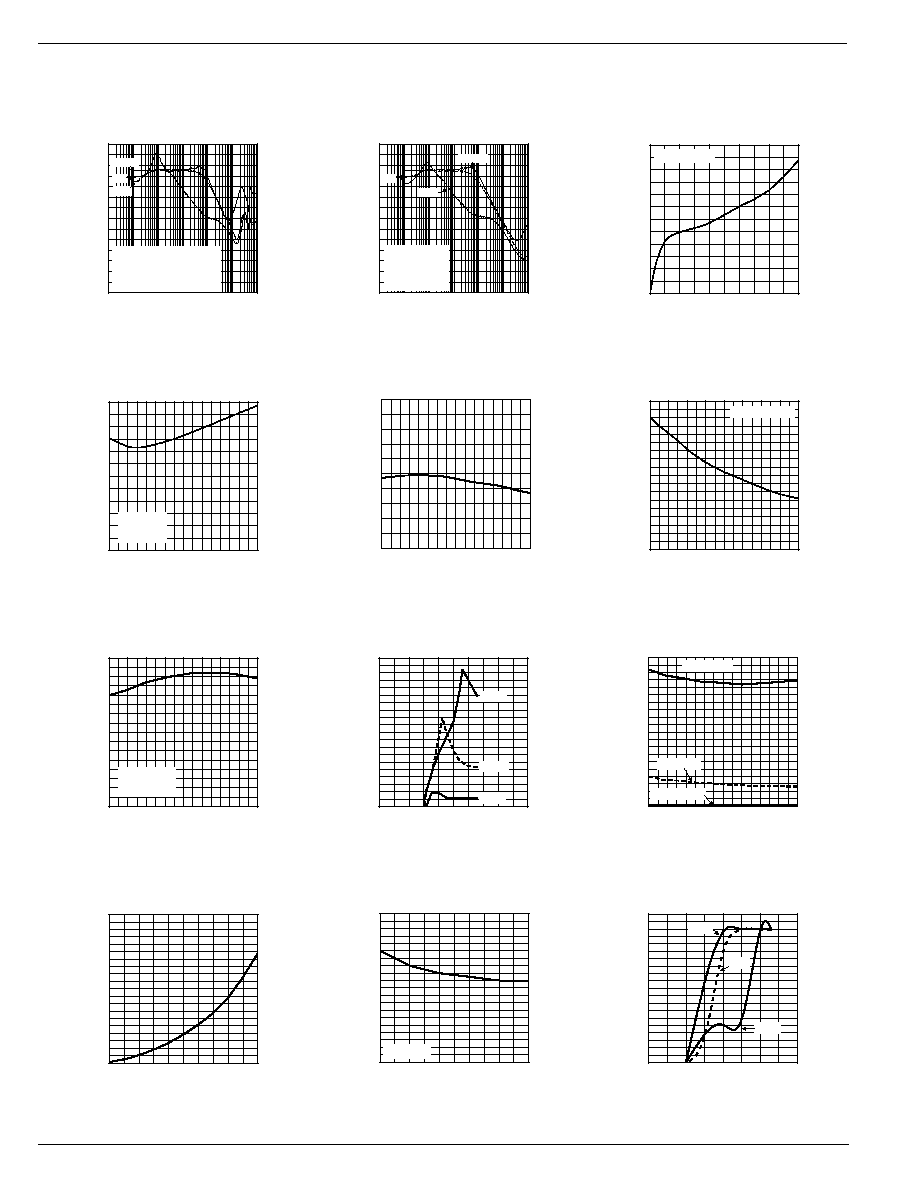
0
10
20
30
40
50
60
70
PRSS (dB)
FREQUENCY (Hz)
PSRR
100mA
1A
2.5A
10
1
100
1k
10k 100k 1M
C
OUT
= 100
µ
F Ceramic
V
IN
= 3.3V
V
OUT
= 1.8V
0
10
20
30
40
50
60
70
PSRR (dB)
FREQUENCY (Hz)
PSRR
100mA
2.5A
1A
1
10
100
1k
10k 100k 1M
C
OUT
= 47
µ
F
V
IN
= 3.3V
V
OUT
= 1.8V
0
100
200
300
400
500
600
0
0.5
1
1.5
2
2.5
DROPOUT VOLTAGE (mV)
OUTPUT CURRENT (A)
Dropout Voltage
V
OUT
= 3.3V
0
100
200
300
400
500
600
-40 -20 0
20 40 60 80 100 120
DROPOUT VOLTAGE (mV)
TEMPERATURE (
∞
C)
Dropout
vs. Temperature
3.3V
OUT
2.5A load
1.75
1.76
1.77
1.78
1.79
1.80
1.81
1.82
1.83
1.84
1.85
-40 -20 0
20 40 60 80 100 120
OUTPUT VOLTAGE (V)
TEMPERATURE (
∞
C)
Output Voltage
vs. Temperature
0
2
4
6
8
10
12
14
16
18
-40 -20 0
20 40 60 80 100 120
ENABLE CURRENT (
µ
A)
TEMPERATURE (
∞
C)
Enable Pin Current
vs. Temperature
100mA Load
0
0.5
1
1.5
2
2.5
3
3.5
4
-40 -20 0
20 40 60 80 100 120
SHORT CIRCUIT CURRENT (A)
TEMPERATURE T
J
(
∞
C)
Short Circuit Current
vs. Temperature
V
OUT
= 0V
V
IN
= 4.3V
0
5
10
15
20
25
30
35
40
45
50
0
1
2
3
4
5
GROUND CURRENT (mA)
SUPPLY VOLTAGE (V)
Ground Current
vs. Supply Voltage
0.5A
1.5A
2.5A
0
5
10
15
20
25
30
35
40
45
50
-40 -20 0
20 40 60 80 100 120
GROUND CURRENT (mA)
TEMPERATURE (
∞
C)
Ground Current
vs. Temperature
1A Load
10mA Load
2.5A Load
Typical Characteristics
0
5
10
15
20
25
30
35
40
45
50
0
0.5
1
1.5
2
2.5
GROUND CURRENT (mA)
OUTPUT CURRENT (A)
Ground Current
vs. Output Current
2.490
2.492
2.494
2.496
2.498
2.500
2.502
2.504
2.506
2.508
2.510
0
0.5
1
1.5
2
2.5
OUTPUT VOLTAGE (V)
OUTPUT CURRENT (A)
Output Voltage
vs. Load Current
2.5V
OUT
0.0
0.2
0.4
0.6
0.8
1.0
1.2
1.4
1.6
1.8
2.0
0
1
2
3
4
OUTPUT VOLTAGE (V)
SUPPLY VOLTAGE (V)
Dropout Characteristics
0.5A
1.5A
2.5A
January 2003
5
MIC37252
MIC37252
Micrel
TIME (400
µ
s/div.)
OUTPUT CURRENT
(1A/div
.
)
OUTPUT V
O
L
T
A
G
E
(100mV/div
.
)
V
IN
= 3.3V
V
OUT
= 1.8V
C
OUT
= 47
µ
F
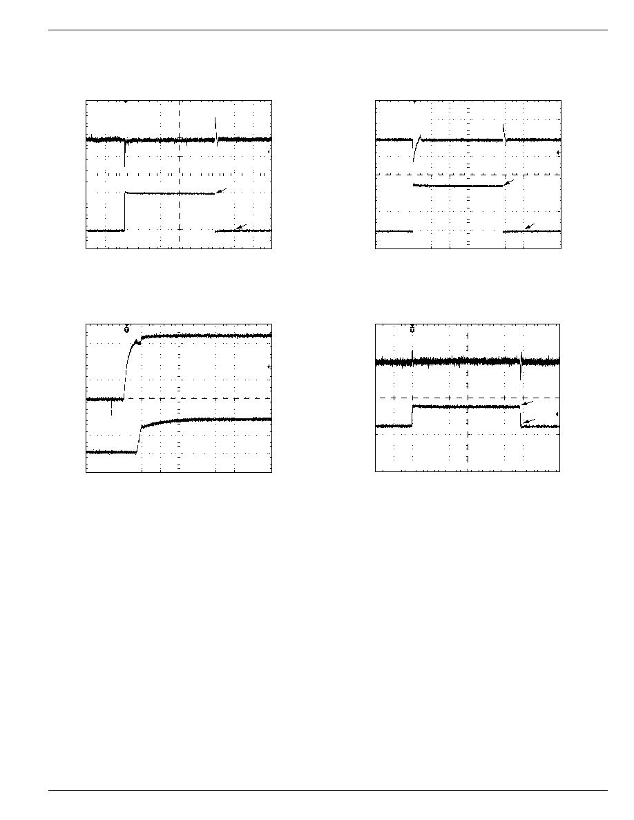
Load Transient Response
10mA
2A
TIME (400
µ
s/div.)
OUTPUT CURRENT
(1A/div
.
)
OUTPUT V
O
L
T
A
G
E
(200mV/div
.
)
V
IN
= 3.3V
V
OUT
= 1.8V
C
OUT
= 47
µ
F
Load Transient Response
10mA
2.5A
MIC37252 Start Up
TIME (100
µ
s/div.)
OUTPUT V
O
L
T
A
G
E
(1V/div
.
)
INPUT V
O
L
T
A
G
E
(1V/div
.
)
Load = 2A
Line Transient Response
TIME (100
µ
s/div.)
OUTPUT V
O
L
T
A
G
E
(20mV/div
.
)
INPUT V
O
L
T
A
G
E
(2V/div
.
)
5V
3.3V
Functional Characteristics

MIC37252
Micrel
MIC37252
6
January 2003
Applications Information
The MIC37252 is a high-performance low-dropout voltage
regulator suitable for moderate to high-current regulator
applications. Its 550mV dropout voltage at full load makes it
especially valuable in battery-powered systems and as high-
efficiency noise filters in post-regulator applications. Unlike
older NPN-pass transistor designs, where the minimum
dropout voltage is limited by the base-to-emitter voltage drop
and collector-to-emitter saturation voltage, dropout perfor-
mance of the PNP output of these devices is limited only by
the low V
CE
saturation voltage.
A trade-off for the low dropout voltage is a varying base drive
requirement. Micrel's Super
eta PNP
process reduces this
drive requirement to only 2% to 5% of the load current.
The MIC37252 regulator is fully protected from damage due
to fault conditions. Current limiting is provided. This limiting is
linear; output current during overload conditions is constant.
Thermal shutdown disables the device when the die tem-
perature exceeds the maximum safe operating temperature.
Transient protection allows device (and load) survival even
when the input voltage spikes above and below nominal. The
output structure of these regulators allows voltages in excess
of the desired output voltage to be applied without reverse
current flow.
Thermal Design
Linear regulators are simple to use. The most complicated
design parameters to consider are thermal characteristics.
Thermal design requires the following application-specific
parameters:
∑ Maximum ambient temperature (T
A
)
∑ Output current (I
OUT
)
∑ Output voltage (V
OUT
)
∑ Input voltage (V
IN
)
∑ Ground current (I
GND
)
First, calculate the power dissipation of the regulator from
these numbers and the device parameters from this datasheet.
P
D
= (V
IN
≠ V
OUT
) I
OUT
+ V
IN
I
GND
where the ground current is approximated by using numbers
from the "Electrical Characteristics" or "Typical Characteris-
tics." Then the heat sink thermal resistance is determined
with this formula:
SA
= ((T
J(MAX)
≠ T
A
)/ P
D
) ≠ (
JC
+
CS
)
Where T
J(MAX)
< 125
o
C and
CS
is between 0
o
C and 2
o
C/W.
The heat sink may be significantly reduced in applications
where the minimum input voltage is known and is large
compared with the dropout voltage. Use a series input
resistor to drop excessive voltage and distribute the heat
between this resistor and the regulator. The low dropout
properties of Micrel Super
eta PNP
regulators allow signifi-
cant reductions in regulator power dissipation and the asso-
ciated heat sink without compromising performance. When
this technique is employed, a capacitor of at least 1.0
µ
F is
needed directly between the input and regulator ground.
Refer to
Application Note 9 for further details and examples
on thermal design and heat sink applications.
Output Capacitor
The MIC37252 requires an output capacitor for stable opera-
tion. As a
µ
Cap LDO, the MIC37252 can operate with ceramic
output capacitors as long as the amount of capacitance is
47
µ
F or greater. For values of output capacitance lower than
47
µ
F, the recommended ESR range is 200m
to 2
. The
minimum value of output capacitance recommended for the
MIC37252 is 10
µ
F.
For 47
µ
F or greater the ESR range recommended is less than
1
. Ultra-low ESR, ceramic capacitors are recommended for
output capacitance of 47
µ
F or greater to help improve tran-
sient response and noise reduction at high frequency. X7R/
X5R dielectric-type ceramic capacitors are recommended
because of their temperature performance. X7R-type capaci-
tors change capacitance by 15% over their operating tem-
perature range and are the most stable type of ceramic
capacitors. Z5U and Y5V dielectric capacitors change value
by as much as 50% and 60% respectively over their operating
temperature ranges. To use a ceramic chip capacitor with
Y5V dielectric, the value must be much higher than an X7R
ceramic capacitor to ensure the same minimum capacitance
over the equivalent operating temperature range. The
MIC37252 has excellent transient response to variations in
input voltage and load current. The device has been designed
to respond quickly to load current variations and input voltage
variations. Large output capacitors are not required to obtain
this performance. A standard 47
µ
F output capacitor is all that
is required. Larger values help to improve performance even
further.
Input Capacitor
An input capacitor of 1.0
µ
F or greater is recommended when
the device is more than 4 inches away from the bulk supply
capacitance, or when the supply is a battery. Small, surface-
mount chip capacitors can be used for the bypassing. The
capacitor should be place within 1" of the device for optimal
performance. Larger values will help to improve ripple rejec-
tion by bypassing the input to the regulator, further improving
the integrity of the output voltage.
Transient Response and 5V to 3.3V or 3.3V to 1.8V
Conversions
The MIC37252 has excellent transient response to variations
in input voltage and load current. The device has been
designed to respond quickly to load current variations and
input voltage variations. Large output capacitors are not
required to obtain this performance. A standard 10
µ
F output
capacitor, preferably tantalum, is all that is required. Larger
values help to improve performance even further.
By virtue of its low-dropout voltage, this device does not
saturate into dropout as readily as similar NPN-based de-
signs. When converting from 3.3V to 1.8V, the NPN-based
regulators are already operating in dropout, with typical
dropout requirements of 2V or greater. To convert down to
1.8V without operating in dropout, NPN-based regulators
require an input voltage of 3.8V at the very least. The
MIC37252 regulator will provide excellent performance with
an input as low as 3.0V. This gives the PNP-based regulators
a distinct advantage over older NPN-based linear regulators.
January 2003
7
MIC37252
MIC37252
Micrel
Minimum Load Current
The MIC37252 regulator is specified between finite loads. If
the output current is too small, leakage currents dominate
and the output voltage rises. A 10mA minimum load current
is necessary for proper operation.
Enable Input
The MIC37252 also features an enable input for on/off control
of the device. Its shutdown state draws "zero" current (only
microamperes of leakage). The enable input is TTL/CMOS
compatible for simple logic interface, but can be connected to
up to V
IN
. When enabled, it draws approximately 15
µ
A.
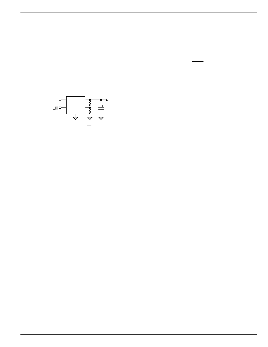
Adjustable Regulator Design
IN
R1
V
OUT
V
IN
C
OUT
R2
EN
OUT
ADJ
GND
MIC37252
ENABLE
SHUTDOWN
V
1.240V 1
R1
R2
OUT
=
+
Figure 2. Adjustable Regulator with Resistors
The MIC37252 allows programming of the output voltage
anywhere between 1.24V and the 5.5V maximum operating
rating of the family. Two resistors are used. Resistors values
are recommended to be less than 10k
in value to improve
stability. The resistor values can be sized to draw the mini-
mum load current for this device. The resistor values are
calculated by:
R1 R2
V
1.240
1
OUT
=
-
Where V
OUT
is the desired output voltage. Figure 2 shows
component definition. Applications with widely varying load
currents may scale the resistors to draw the minimum load
current required for proper operation (see above).
MIC37252
Micrel
MIC37252
8
January 2003
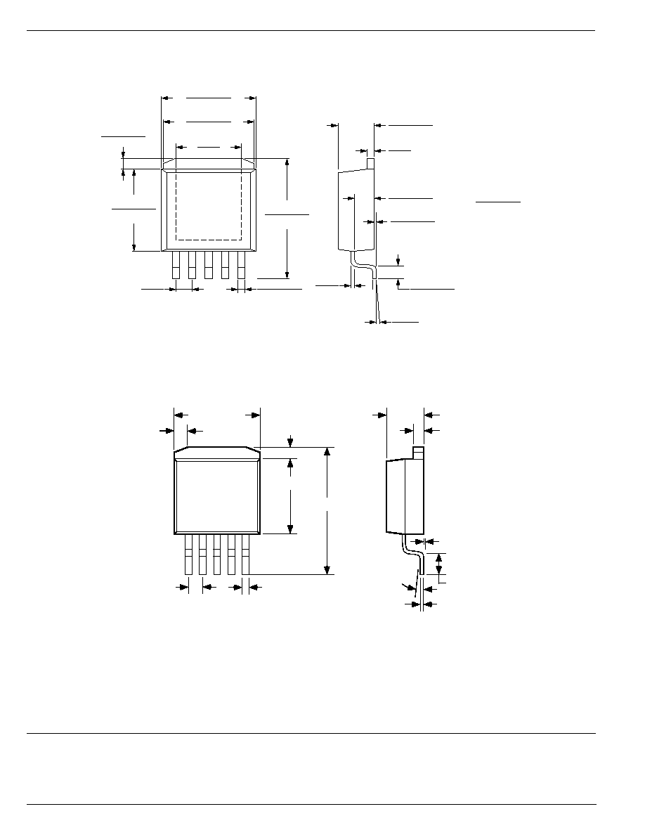
Package Information
0.370
±
0.005
9.395
±
0.125
0.355
±
0.005
9.015
±
0.125
0.315
±
0.005
8.000
±
0.130
0.415
±
0.005
10.54
±
0.130
0.028
±
0.003
0.710
±
0.080
0.075
±
0.005
1.905
±
0.125
0.040
±
0.005
1.015
±
0.125
0.003
±
0.002
0.080
±
0.050
0.036
±
0.005
0.915
±
0.125
INCHES
MILLIMETER
0
∞
min
6
∞
max
0.010
0.250
0.010
0.250
0.067
1.700
0.040
±
0.010
1.015
±
0.255
0.256
6.50
5-Lead S-PAK (R)
0.067
±
0.005
0.032
±
0.003
0.360
±
0.005
0.600
±
0.025
0.405
±
0.005
0.060
±
0.005
0.176
±
0.005
8
∞
MAX
0.100
±
0.01
0.050
±
0.005
0.015
±
0.002
0.004+0.004
≠0.008
SEATING PLANE
0.065
±
0.010
20
∞±
2
∞
DIM. = INCH
5-Lead TO-263 (U)
MICREL, INC.
1849 FORTUNE DRIVE
SAN JOSE, CA 95131
USA
TEL
+ 1 (408) 944-0800
FAX
+ 1 (408) 944-0970
WEB
http://www.micrel.com
This information is believed to be accurate and reliable, however no responsibility is assumed by Micrel for its use nor for any infringement of patents or
other rights of third parties resulting from its use. No license is granted by implication or otherwise under any patent or patent right of Micrel, Inc.
© 2002 Micrel, Incorporated