
November 2003
1
M0307-112003
MIC37300/37301/37302
Micrel
MIC37300/37301/37302
3.0A, Low-Voltage
µ
Cap LDO Regulator
General Description
The Micrel MIC37300/01/02 is a 3.0A low-dropout linear
voltage regulator that provides a low-voltage, high-current
output with a minimum number of external components. It
offers high precision, ultra-low-dropout (500mV overtem-
perature), and low-ground current.
The MIC37300/01/02 operates from an input of 2.25V to
6.0V. It is designed to drive digital circuits requiring low-
voltage at high currents (i.e., PLDs, DSP, microcontroller,
etc.). It is available in fixed and adjustable output voltages.
Fixed voltages include 1.5V, 1.8V, 2.5V and 3.3V. The
adjustable version is capable of 1.24V to 5.5V.
Features of the MIC37300/01/02 LDO include thermal and
current-limit protection, and reverse-current protection. Logic
enable and error flag pins are available on the 5-pin version.
Junction temperature range of the MIC37300/01/02 is from
≠40
∞
C to 125
∞
C.
For applications requiring input voltage greater than 6.0V,
see the MIC3910x, MIC3915x, MIC3930x, and MIC3950x
LDOs.
All data sheets and support documentation can be found
on Micrel's web site at www.micrel.com.
Typical Application
VOUT
VIN
GND
C
OUT
47
µ
F, Ceramic
MIC37300
V
IN
= 3.0V
V
OUT
= 2.5V
Fixed 2.5V Regulator
VOUT
VIN
FLG
GND
VEN
C
OUT
47
µ
F, Ceramic
100k
MIC37301
V
IN
= 3.0V
V
OUT
= 2.5V
C
IN
Fixed 2.5V Regulator with Error Flag
Features
∑ 3.0A minimum guaranteed output current
∑ 500mV maximum dropout-voltage overtemperature
Ideal for 3.0V to 2.5V conversion
Ideal for 2.5V to 1.8V, 1.65V, or 1.5V conversion
∑ Stable with ceramic or tantalum capacitor
∑ Wide input voltage range:
V
IN
: 2.25V to 6.0V
∑ +1.0% initial output tolerance
∑ Fixed and adjustable output voltages:
MIC37300 -- 3-pin fixed
MIC37301 -- 5-pin fixed with flag
MIC37302 -- 5-pin adjustable
∑ Excellent line and load regulation specifications
∑ Logic controlled shutdown
∑ Thermal shutdown and current-limit protection
∑ Reverse-leakage protection
∑ Low profile S-Pak package
Applications
∑ LDO linear regulator for low-voltage digital IC
∑ PC add-in cards
∑ High-efficiency linear power supplies
∑ SMPS post regulator
∑ Battery charger
Micrel, Inc. ∑ 1849 Fortune Drive ∑ San Jose, CA 95131 ∑ USA ∑ tel + 1 (408) 944-0800 ∑ fax + 1 (408) 944-0970 ∑ http://www.micrel.com
Super þeta PNP is a registered trademark of Micrel, Inc.
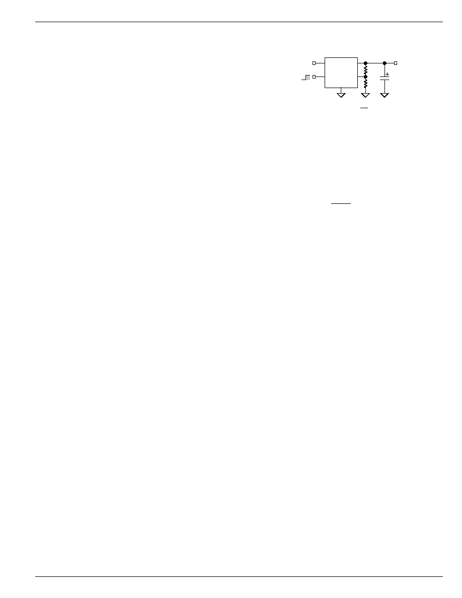
VOUT
VIN
ADJ
GND
VEN
C
OUT
47
µ
F, Ceramic
R1
R2
1.3V
MIC37302
V
IN
C
IN
Adjustable Regulator
0
50
100
150
200
250
300
350
400
450
500
0
0.5
1
1.5
2
2.5
3
DROPOUT (mV)
OUTPUT CURRENT (A)
Dropout vs.
Output Current
2.5V
OUT
3.3V
OUT
MIC37300/37301/37302
Micrel
M0307-112003
2
November 2003
Ordering Information
Output
Part Number
Current
Voltage*
Junction Temp. Range
Package
MIC37300-1.5BR
3.0A
1.5V
≠40
∞
C to +125
∞
C
S-Pak-3
MIC37300-1.65BR
3.0A
1.65V
≠40
∞
C to +125
∞
C
S-Pak-3
MIC37300-1.8BR
3.0A
1.8V
≠40
∞
C to +125
∞
C
S-Pak-3
MIC37300-2.5BR
3.0A
2.5V
≠40
∞
C to +125
∞
C
S-Pak-3
MIC37300-3.3BR
3.0A
3.3V
≠40
∞
C to +125
∞
C
S-Pak-3
MIC37301-1.5BR
3.0A
1.5V
≠40
∞
C to +125
∞
C
S-Pak-5
MIC37301-1.8BR
3.0A
1.8V
≠40
∞
C to +125
∞
C
S-Pak-5
MIC37301-2.5BR
3.0A
2.5V
≠40
∞
C to +125
∞
C
S-Pak-5
MIC37301-3.3BR
3.0A
3.3V
≠40
∞
C to +125
∞
C
S-Pak-5
MIC37302BR
3.0A
ADJ.
≠40
∞
C to +125
∞
C
S-Pak-5
MIC37302BU
3.0A
ADJ.
≠40
∞
C to +125
∞
C
TO-263-5
*For other voltages contact Micrel.
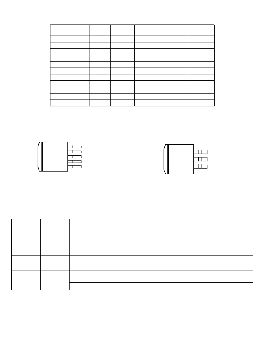
Pin Configuration
TA
B
5
FLG/ADJ
4
VOUT
3
GND
2
VIN
1
EN
S-PAK-5 (R)
TO-263-5 (U)
TA
B
3
VOUT
2
GND
1
VIN
S-PAK-3 (R)
Pin Description
Pin Number
Pin Number
Pin Name
Pin Function
TO-263-5
S-PAK-3
S-PAK-5
1
EN
Enable (Input): CMOS compatible input. Logic high = enable, logic
low = shutdown.
2
1
VIN
Input voltage which supplies current to the output power device.
3
2
GND
Ground: TAB is connected to ground.
4
3
VOUT
Regulator Output.
5
FLG
Error Flag (Output): Open collector output. Active-low indicates an output
fault condition.
ADJ
Adjustable Regulator Feedback Input: Connect to resistor voltage divider.

November 2003
3
M0307-112003
MIC37300/37301/37302
Micrel
Electrical Characteristics
(5)
T
A
= 25
∞
C with V
IN
= V
OUT
+ 1V; V
EN
= V
IN
; I
L
= 10mA; bold values indicate ≠40
∞
C < T
J
< +125
∞
C; unless otherwise noted.
Parameter
Condition
Min
Typ
Max
Units
Output Voltage Accuracy
I
L
= 10mA
≠1
+1
%
10mA < I
OUT
< I
L
(max), V
OUT
+ 1
V
IN
6V
≠2
+2
%
Output Voltage Line Regulation
V
IN
= V
OUT
+1.0V to 6.0V, I
L
= 10mA
0.02
0.5
%
Output Voltage Load Regulation
I
L
= 10mA to 3A
0.2
1
%
V
IN
≠ V
OUT
; Dropout Voltage
(6)
I
L
= 1.5A
175
350
mV
I
L
= 3A
310
500
mV
Ground Pin Current
(7)
I
L
= 3A
27
40
mA
50
mA
Ground Pin Current in Shutdown
V
IL
< 0.5V, V
IN
= V
OUT
+ 1V
1.0
5
µ
A
Current Limit
V
OUT
= 0
4.75
6.5
A
Start-up Time
V
EN
= V
IN
, I
OUT
= 10mA, C
OUT
= 47
µ
F
170
500
µ
s
Enable Input
Enable Input Threshold
Regulator enable
2.25
V
Regulator shutdown
0.8
V
Enable Pin Input Current
V
IL
< 0.8V (Regulator shutdown)
2
µ
A
4
µ
A
V
IH
> 2.25V (Regulator enabled)
1
15
30
µ
A
75
µ
A
Flag Output
I
FLG(LEAK)
V
OH
= 6V
1
µ
A
2
µ
A
V
FLG(LO)
V
IN
= 2.25V, I
OL
= 250
µ
A
(8)
210
400
mV
500
mV
V
FLG
Low Threshold, % of V
OUT
below nominal
93
%
Hysteresis
2
%
High Threshold, % of V
OUT
below nominal
99.2
%
MIC37302 Only
Reference Voltage
1.228
1.240
1.252
V
1.215
1.265
V
Adjust Pin Bias Current
40
80
nA
120
nA
Notes:
1.
Exceeding the absolute maximum ratings may damage the device.
2.
The device is not guaranteed to function outside its operating rating.
3.
P
D
(max) = (T
J
(max) ≠ T
A
) /
JA
, where
JA
, depends upon the printed circuit layout. See
"Applications Information."
4.
Device is ESD sensitive. Handling precautions recommended.
5.
Specification for packaged product only.
Absolute Maximum Rating
(1)
Supply Voltage (V
IN
) .................................................... 6.5V
Enable Input Voltage (V
EN
)
(3) ................................................
6.5V
Power Dissipation (P
D
)
(3) ...............................
Internally Limited
Junction Temperature (T
J
) ................. ≠40
∞
C
T
J
+125
∞
C
Storage Temperature (T
S
) ................. ≠65
∞
C
T
J
+150
∞
C
Lead Temperature (soldering, 5 sec.) ....................... 260
∞
C
ESD
(4)
Operating Maximum Rating
(2)
Supply Voltage (V
IN
) ..................................... 2.25V to 6.0V
Enable Input Voltage (V
EN
) ................................ 0V to 6.0V
Junction Temperature Range (T
J
) ..... ≠40
∞
C
T
J
+125
∞
C
Package Thermal Resistance
S-Pak (
JC
) ........................................................ 2
∞
C/W
TO-263-5 (
JC
) .................................................. 2
∞
C/W

MIC37300/37301/37302
Micrel
M0307-112003
4
November 2003
Notes:
6.
V
DO
= V
IN
≠ V
OUT
when V
OUT
decreased to 98% of its nominal output voltage with V
IN
= V
OUT
+1V. For output voltages below 1.75V, dropout
voltage specification does not apply due to a minimum input operating voltage of 2.25V.
7.
I
GND
is the quiescent current. I
IN
= I
GND
+ I
OUT
.
8.
For a 2.5V device, V
IN
= 2.250V (device is in dropout).
November 2003
5
M0307-112003
MIC37300/37301/37302
Micrel
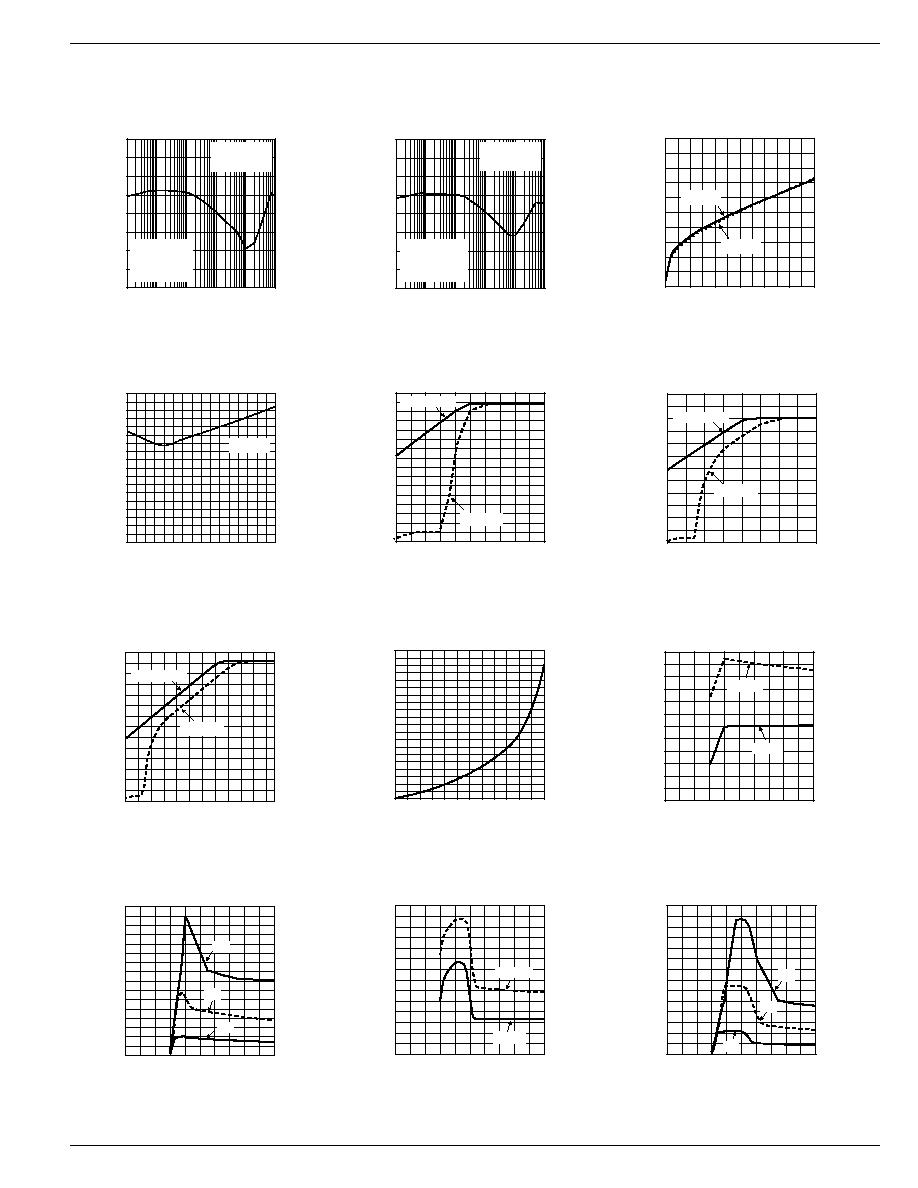
Typical Characteristics
0
10
20
30
40
50
60
70
80
0.01
0.1
1
10
100
1000
PSRR (dB)
FREQUENCY (kHz)
Power Supply
Rejection Ratio
I
OUT
= 3A
C
OUT
= 47
µ
F
C
IN
= 0
V
IN
= 2.5V
V
OUT
= 1.5V
0
10
20
30
40
50
60
70
80
0.01
0.1
1
10
100
1000
PSRR (dB)
FREQUENCY (kHz)
Power Supply
Rejection Ratio
I
OUT
= 3A
C
OUT
= 100
µ
F
C
IN
= 0
V
IN
= 2.5V
V
OUT
= 1.5V
0
50
100
150
200
250
300
350
400
450
500
0
0.5
1
1.5
2
2.5
3
DROPOUT (mV)
OUTPUT CURRENT (A)
Dropout vs.
Output Current
2.5V
OUT
3.3V
OUT
0
50
100
150
200
250
300
350
400
450
-40 -20 0
20 40 60 80 100 120
DROPOUT (mV)
TEMPERATURE (
∞
C)
Dropout vs.
Temperature
2.5V
OUT
0
0.2
0.4
0.6
0.8
1
1.2
1.4
1.6
1.5
1.7
1.9
2.1
2.3
2.5
OUTPUT VOLTAGE (V)
INPUT VOLTAGE (V)
Dropout Characteristics
(1.5V)
3A Load
10mA Load
0
0.5
1
1.5
2
2.5
3
1.5
2
2.5
3
3.5
OUTPUT VOLTAGE (V)
INPUT VOLTAGE (V)
Dropout Characteristics
(2.5V)
3A Load
10mA Load
0
0.5
1
1.5
2
2.5
3
3.5
1.5
2
2.5
3
3.5
4
OUTPUT VOLTAGE (V)
INPUT VOLTAGE (V)
Dropout Characteristics
(3.3V)
3A Load
10mA Load
0
5
10
15
20
25
30
35
40
45
50
0
0.5
1
1.5
2
2.5
3
GROUND CURRENT (mA)
OUTPUT CURRENT (A)
Ground Current
vs. Output Current
0
0.0001
0.0002
0.0003
0.0004
0.0005
0.0006
0
1
2
3
4
5
GROUND CURRENT (mA)
SUPPLY VOLTAGE (V)
Ground Current
vs. Supply Voltage (1.5V)
100mA
10mA
0
5
10
15
20
25
30
35
40
0
1
2
3
4
5
GROUND CURRENT (mA)
SUPPLY VOLTAGE (V)
Ground Current
vs. Supply Voltage (1.5V)
3A
2A
1A
0
10
20
30
40
50
60
70
0
1
2
3
4
5
GROUND CURRENT (mA)
SUPPLY VOLTAGE (V)
Ground Current
vs. Supply Voltage (2.5V)
3A
2A
1A
0
0.2
0.4
0.6
0.8
1
1.2
1.4
0
1
2
3
4
5
GROUND CURRENT (mA)
SUPPLY VOLTAGE (V)
Ground Current
vs. Supply Voltage (2.5V)
100mA
10mA
MIC37300/37301/37302
Micrel
M0307-112003
6
November 2003
0
0.2
0.4
0.6
0.8
1
1.2
1.4
0
1
2
3
4
5
GROUND CURRENT (mA)
SUPPLY VOLTAGE (V)
Ground Current
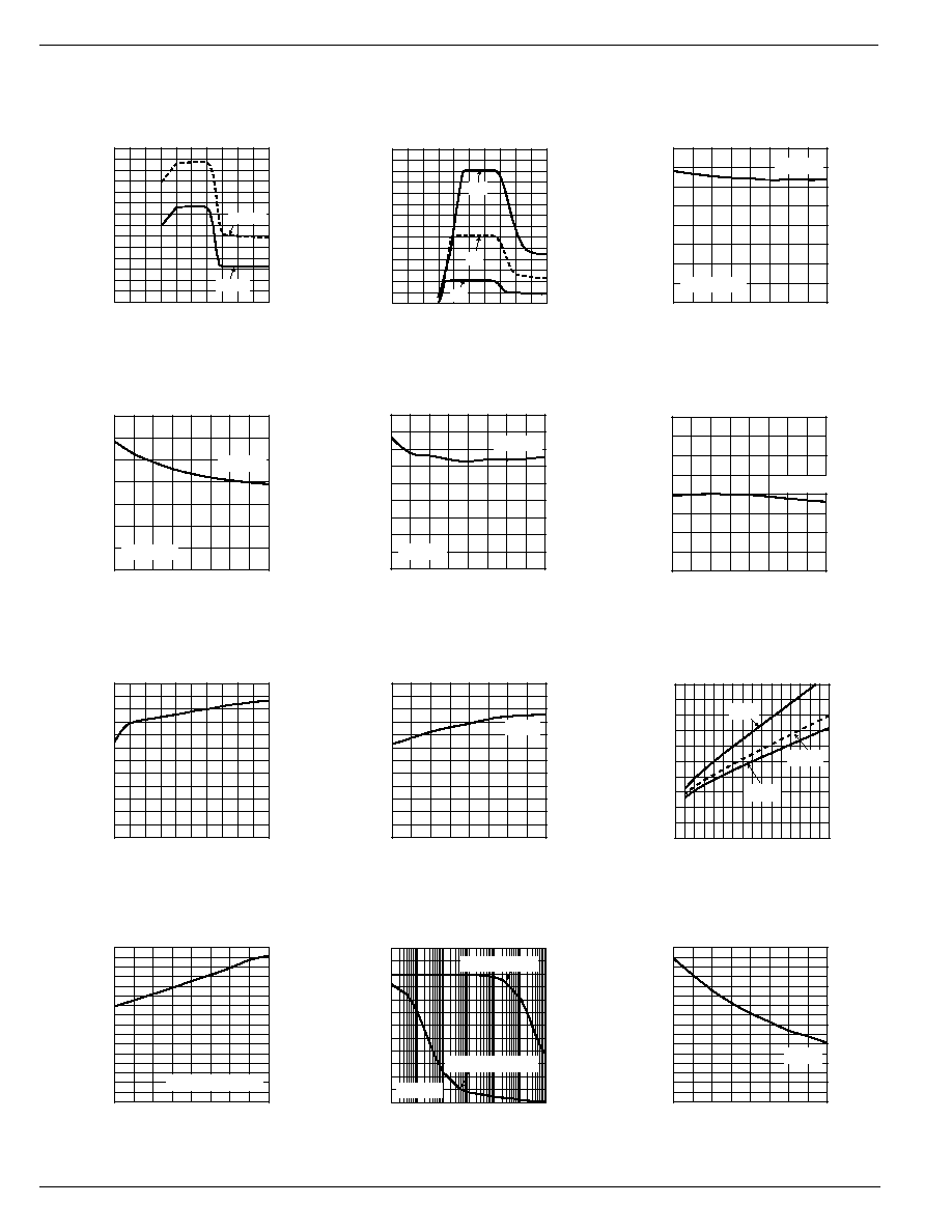
vs. Supply Voltage (3.3V)
100mA
10mA
0
10
20
30
40
50
60
70
0
1
2
3
4
5
GROUND CURRENT (mA)
SUPPLY VOLTAGE (V)
Ground Current
vs. Supply Voltage (3.3V)
3A
2A
1A
0
2
4
6
8
10
12
14
-40 -20 0
20 40 60 80 100 120
GROUND CURRENT (mA)
TEMPERATURE (
∞
C)
Ground Current
vs. Temperature
IOUT=1.5A
2.5VOUT
0
5
10
15
20
25
30
35
40
45
-40 -20 0
20 40 60 80 100 120
GROUND CURRENT (mA)
TEMPERATURE (
∞
C)
Ground Current
vs. Temperature
IOUT=3A
2.5VOUT
2.4
2.45
2.5
2.55
2.6
-40 -20 0
20 40 60 80 100 120
OUTPUT VOLTAGE (V)
TEMPERATURE (
∞
C)
Output Voltage
vs. Temperature
2.5VOUT
0
0.05
0.1
0.15
0.2
0.25
0.3
0.35
0.4
-40 -20 0
20 40 60 80 100 120
GROUND CURRENT (mA)
TEMPERATURE (
∞
C)
Ground Current
vs. Temperature
IOUT=10mA
2.5VOUT
0
0.5
1
1.5
2
2.5
3
3.5
4
4.5
5
5.5
6
2.25
3
3.75
4.5
5.25
6
SHORT CIRCUIT CURRENT (A)
SUPPLY VOLTAGE (V)
Short-Circuit Current
vs. Supply Voltage
0
1
2
3
4
5
6
-40 -20 0
20 40 60 80 100 120
SHORT CIRCUIT CURRENT (A)
TEMPERATURE (
∞
C)
Short-Circuit Current
vs. Temperature
2.5V
IN
0
0.2
0.4
0.6
0.8
1.0
0 0.5 1 1.5 2 2.5 3 3.5 4
FLAG VOLTAGE (V)
FLAG CURRENT (mA)
Flag Voltage
vs. Flag Current
5V
IN
3.3V
IN
2.5V
IN
0
50
100
150
200
250
300
350
400
-40 -20 0
20 40 60 80 100 120
FLAG VOLTAGE (mV)
TEMPERATURE (
∞
C)
Flag Low Voltage
vs. Temperature
Flag Current=250
µ
A
0
1
2
3
4
5
6
0.01
0.1
1
10
100 1000 10000
FLAG VOLTAGE (V)
RESISTANCE (k
)
Error Flag Pull-Up Resistor
Flag Low (FAULT)
Flag High (OK)
V
IN
= 5V
0
2
4
6
8
10
12
14
16
-40 -20 0
20 40 60 80 100 120
ENABLE CURRENT (
µ
A)
TEMPERATURE (
∞
C)
Enable Current
vs. Temperature
2.5V
EN
November 2003
7
M0307-112003
MIC37300/37301/37302
Micrel
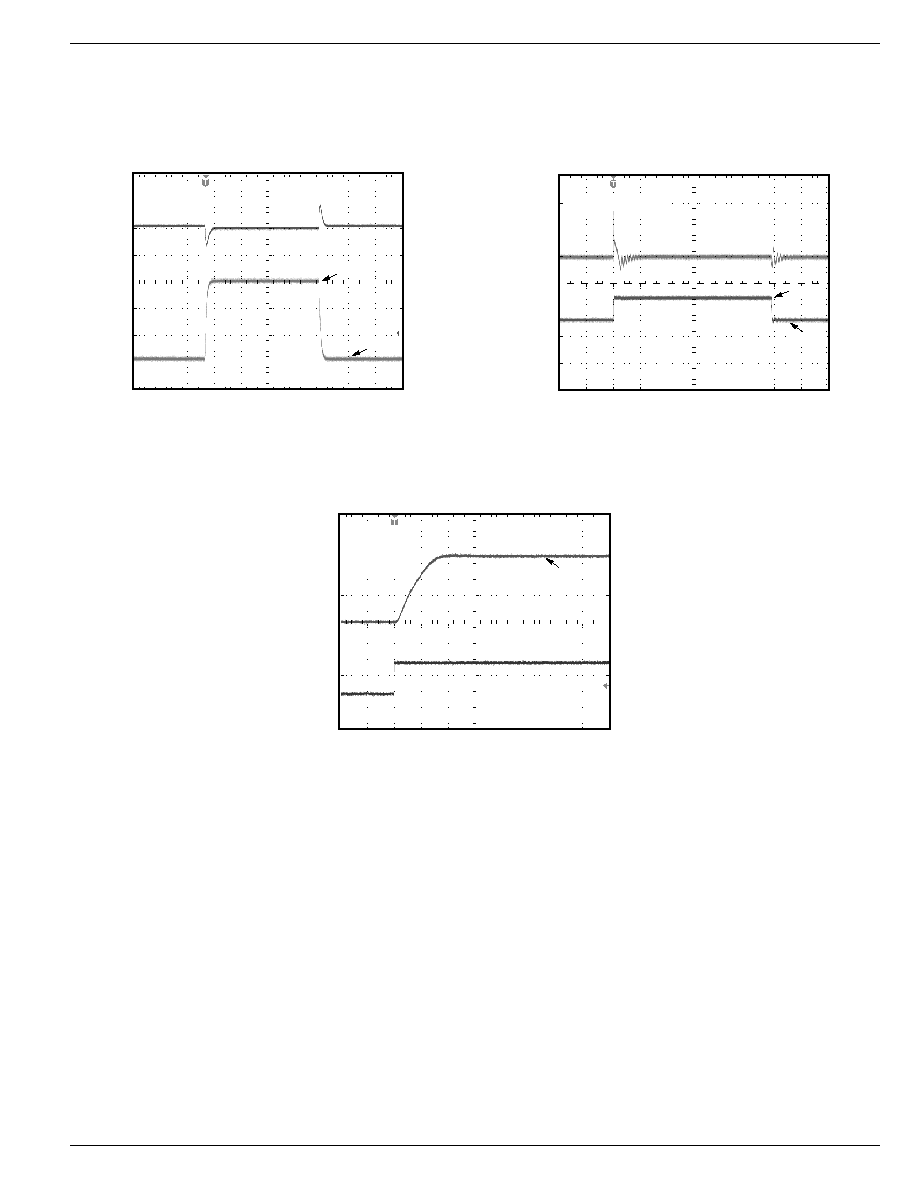
Functional Characteristics
TIME (400
µ
s/div.)
OUTPUT
CURRENT
(3A/div
.)
OUTPUT
VOL
T
AGE
(50mV/div
.)
V
IN
= 3.3V
V
OUT
= 2.5V
C
OUT
= 47
µ
F Ceramic
Load Transient Response
10mA
3A
TIME (100
µ
s/div.)
INPUT
VOL
T
AGE
(2V/div
.)
OUTPUT
VOL
T
AGE
(50mV/div
.)
C
OUT
= 47
µ
F Ceramic
Line Transient Response
3.3V
5V
TIME (40
µ
s/div.)
ENABLE
VOL
T
AGE
(2V/div
.)
OUTPUT
VOL
T
AGE
(1V/div
.)
I
OUT
= 3A
V
IN
= 3.3V
C
OUT
= 47
µ
F
Enable Transient Response
2.5V

MIC37300/37301/37302
Micrel
M0307-112003
8
November 2003
Applications Information
The MIC37300/01/02 is a high-performance low-dropout
voltage regulator suitable for moderate to high-current regu-
lator applications. Its 500mV dropout voltage at full load and
overtemperature makes it especially valuable in battery-
powered systems and as high-efficiency noise filters in post-
regulator applications. Unlike older NPN-pass transistor de-
signs, there the minimum dropout voltage is limited by the
based-to-emitter voltage drop and collector-to-emitter satu-
ration voltage, dropout performance of the PNP output of
these devices is limited only by the low V
CE
saturation
voltage.
A trade-off for the low dropout voltage is a varying base drive
requirement. Micrel's Super þeta PNP
process reduces this
drive requirement to only 2% to 5% of the load current.
The MIC37300/01/02 regulator is fully protected from dam-
age due to fault conditions. Current limiting is provided. This
limiting is linear; output current during overload conditions is
constant. Thermal shutdown disables the device when the
die temperature exceeds the maximum safe operating tem-
perature. The output structure of these regulators allows
voltages in excess of the desired output voltage to be applied
without reverse current flow.
Thermal Design
Linear regulators are simple to use. The most complicated
design parameters to consider are thermal characteristics.
Thermal design requires the following application-specific
parameters:
∑ Maximum ambient temperature (T
A
)
∑ Output current (I
OUT
)
∑ Output voltage (V
OUT
)
∑ Input voltage (V
IN
)
∑ Ground current (I
GND
)
First, calculate the power dissipation of the regulator from
these numbers and the device parameters from this datasheet.
P
D
= (V
IN
≠ V
OUT
) I
OUT
+ V
IN
I
GND
where the ground current is approximated by using numbers
from the
"Electrical Characteristics"
or
"Typical Characteris-
tics."
Then the heat sink thermal resistance is determined
with this formula:
SA
=
(
(T
J
(max) ≠ T
A
)/ P
D
)
≠
(
JC
+
CS
)
Where T
J
(max) < 125
∞
C and
CS
is between 0
∞
C and 2
∞
C/W.
The heat sink may be significantly reduced in applications
where the minimum input voltage is known and is large
compared with the dropout voltage. Use a series input
resistor to drop excessive voltage and distribute the heat
between this resistor and the regulator. The low-dropout
properties of Micrel's Super þeta PNP
regulators allow
significant reductions in regulator power dissipation and the
associated heat sink without compromising performance.
When this technique is employed, a capacitor of at least
1.0
µ
F is needed directly between the input and regulator
ground.
Refer to
"Application Note 9"
for further details and examples
on thermal design and heat sink applications.
Output Capacitor
The MIC37300/01/02 requires an output capacitor for stable
operation. As a
µ
Cap LDO, the MIC37300/01/02 can operate
with ceramic output capacitors as long as the amount of
capacitance is 47
µ
F or greater. For values of output capaci-
tance lower than 47
µ
F, the recommended ESR range is
200m
to 2
. The minimum value of output capacitance
recommended for the MIC37300 is 10
µ
F.
For 47
µ
F or greater, the ESR range recommended is less
than 1
. Ultra-low ESR, ceramic capacitors are recom-
mended for output capacitance of 47
µ
F or greater to help
improve transient response and noise reduction at high
frequency. X7R/X5R dielectric-type ceramic capacitors are
recommended because of their temperature performance.
X7R-type capacitors change capacitance by 15% over their
operating temperature range and are the most stable type of
ceramic capacitors. Z5U and Y5V dielectric capacitors change
value by as much as 50% and 60%, respectively, over their
operating temperature ranges. To use a ceramic chip capaci-
tor with Y5V dielectric, the value must be much higher than an
X7R ceramic capacitor to ensure the same minimum capaci-
tance over the equivalent operating temperature range.
Input Capacitor
An input capacitor of 1.0
µ
F or greater is recommended when
the device is more than 4 inches away from the bulk supply
capacitance, or when the supply is a battery. Small, surface-
mount chip capacitors can be used for the bypassing. The
capacitor should be place within 1" of the device for optimal
performance. Larger values will help to improve ripple rejec-
tion by bypassing the input to the regulator, further improving
the integrity of the output voltage.
Transient Response and 3.3V to 2.5V, 2.5V to 1.8V or
1.65V, or 2.5V to 1.5V Conversions
The MIC37300/01/02 has excellent transient response to
variations in input voltage and load current. The device has
been designed to respond quickly to load current variations
and input voltage variations. Large output capacitors are not
required to obtain this performance. A standard 47
µ
F output
capacitor, preferably tantalum, is all that is required. Larger
values help to improve performance even further.
By virtue of its low-dropout voltage, this device does not
saturate into dropout as readily as similar NPN-based
designs. When converting from 3.3V to 2.5V, 2.5V to 1.8V or
1.65V, or 2.5V to 1.5V, the NPN-based regulators are already
operating in dropout, with typical dropout requirements of
1.2V or greater. To convert down to 2.5V without operating in
dropout, NPN-based regulators require an input voltage of
3.7V at the very least. The MIC37300/01/02 regulator will
provide excellent performance with an input as low as 3.0V or
2.25V, respectively. This gives the PNP-based regulators a
distinct advantage over older, NPN-based linear regulators.
November 2003
9
M0307-112003
MIC37300/37301/37302
Micrel
Minimum Load Current
The MIC37300/01/02 regulator is specified between finite
loads. If the output current is too small, leakage currents
dominate and the output voltage rises. A 10mA minimum load
current is necessary for proper operation.
Error Flag
The MIC37301 features an error flag circuit that monitors the
output voltage and signals an error condition when the
voltage is 5% below the nominal output voltage. The error flag
is an open-collector output that can sink 10mA during a fault
condition.
Low output voltage can be caused by a number of problems,
including an overcurrent fault (device in current limit) or low
input voltage. The flag is inoperative during overtemperature
shutdown.
Enable Input
The MIC37301/37302 also features an enable input for on/off
control of the device. Its shutdown state draws "zero" current
(only microamperes of leakage). The enable input is TTL/
CMOS compatible for simple logic interface, but can be
connected up to V
IN
. When enabled, it draws approximately
15
µ
A.
Adjustable Regulator Design
IN
R1
V
OUT
V
IN
C
OUT
R2
EN
OUT
ADJ
GND
MIC37302
ENABLE
SHUTDOWN
V
1.240V 1
R1
R2
OUT
=
+
Figure 2. Adjustable Regulator with Resistors
The MIC37302 allows programming the output voltage any-
where between 1.24V and the 5.5V maximum operating
rating of the family. Two resistors are used. Resistors can be
quite large, up to 1M
, because of the very high input
impedance and low bias current of the sense comparator.
The resistor values are calculated by:
R1 R2
V
1.240
1
OUT
=
-
Where V
OUT
is the desired output voltage. Figure 2 shows
component definition. Applications with widely varying load
currents may scale the resistors to draw the minimum load
current required for proper operation (see above).
MIC37300/37301/37302
Micrel
M0307-112003
10
November 2003
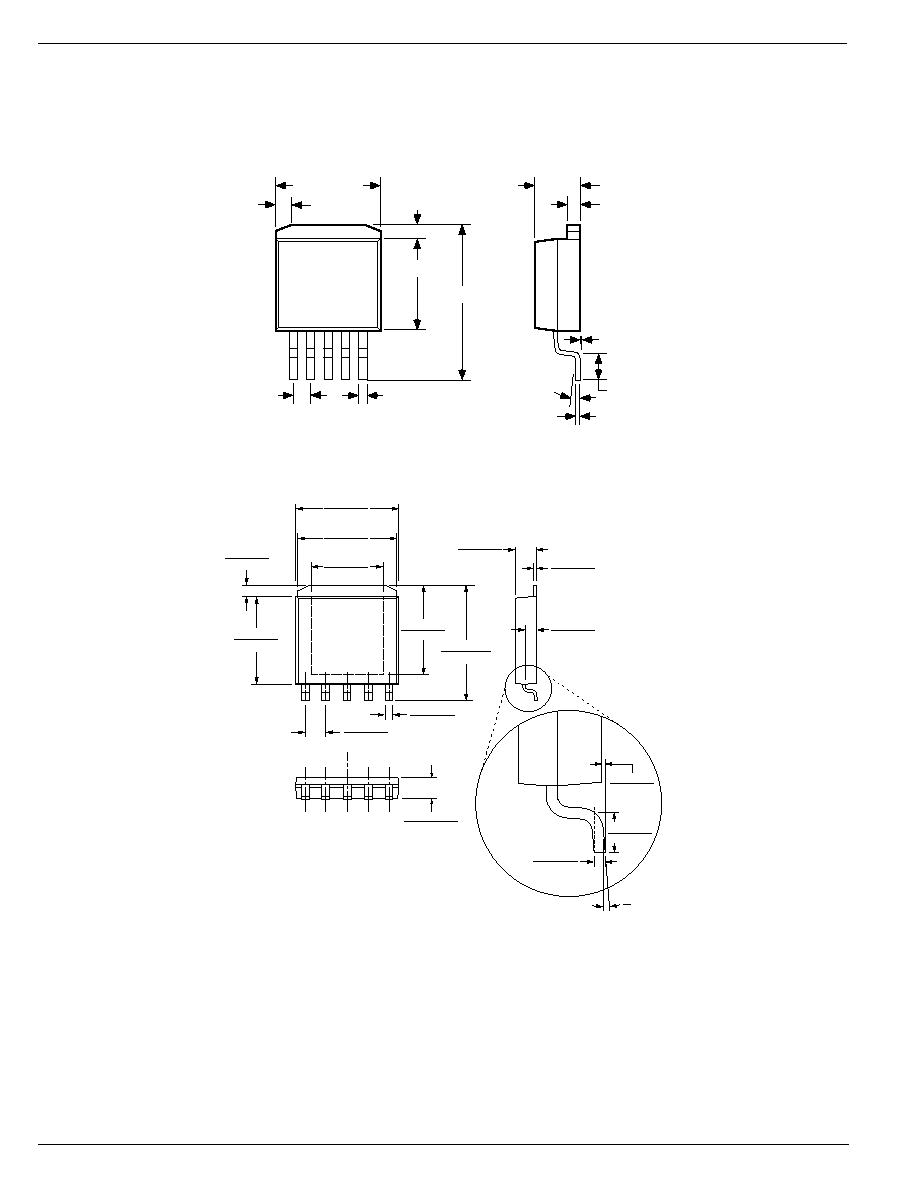
Package Information
0.067
±
0.005
0.032
±
0.003
0.360
±
0.005
0.600
±
0.025
0.405
±
0.005
0.060
±
0.005
0.176
±
0.005
8
∞
MAX
0.100
±
0.01
0.050
±
0.005
0.015
±
0.002
0.004+0.004
≠0.008
SEATING PLANE
0.065
±
0.010
20
∞±
2
∞
DIM. = INCH
5-Lead TO-263-5 (U)
0.375 (9.52)
0.365 (9.27)
0.360 (9.14)
0.350 (8.89)
0.080 (2.03)
0.070 (1.78)
0.010 BSC
(0.25 BSC)
0.045 (1.14)
0.035 (0.89)
0.316 BSC
(8.03 BSC)
0.256 BSC
(6.50 BSC)
0.031 (0.79)
0.025 (0.63)
0.005 (0.13)
0.001 (0.03)
6°
0°
0.010 BSC
(0.25 BSC)
0.067 BSC
(1.70 BSC)
0.031 (0.89)
0.041 (1.14)
0.420 (10.67)
0.410 (10.41)
0.050 (1.27)
0.030 (0.76)
0.320 (8.13)
0.310 (7.87)
DIMENSIONS:
INCH (MM)
0.080 (2.03)
0.070 (1.78)
5-Lead S-PAK (R)

November 2003
11
M0307-112003
MIC37300/37301/37302
Micrel
0.256 BSC
(6.50 BSC)
0.360 (9.14)
0.350 (8.89)
0.375 (9.52)
0.365 (9.27)
0.031 (0.79)
0.025 (0.63)
0.080 (2.03)
0.070 (1.78)
0.008 (0.20)
0.004 (0.10)
0.316 BSC
(8.03 BSC)
0.420 (0.20)
0.410 (0.10)
0.420 (0.20)
0.410 (0.10)
0.041 (1.04)
0.031 (0.79)
0.010 BSC
(0.25 BSC)
6°
0°
0.100 BSC
(2.54 BSC)
0.041 (1.04)
0.031 (0.79)
0.010 BSC
(0.25 BSC)
0.035 (0.89)
0.045 (1.14)
0.320 (8.13)
0.310 (7.87)
0.050 (1.27)
0.030 (0.76)
"A"
DETAIL "A"
3-Lead S-PAK (R)

MIC37300/37301/37302
Micrel
M0307-112003
12
November 2003
MICREL, INC.
1849 FORTUNE DRIVE
SAN JOSE, CA 95131
USA
TEL
+ 1 (408) 944-0800
FAX
+ 1 (408) 944-0970
WEB
http://www.micrel.com
The information furnished by Micrel in this datasheet is believed to be accurate and reliable. However, no responsibility is assumed by Micrel for its use.
Micrel reserves the right to change circuitry and specifications at any time without notification to the customer.
Micrel Products are not designed or authorized for use as components in life support appliances, devices or systems where malfunction of a product can
reasonably be expected to result in personal injury. Life support devices or systems are devices or systems that (a) are intended for surgical implant into
the body or (b) support or sustain life, and whose failure to perform can be reasonably expected to result in a significant injury to the user. A Purchaser's
use or sale of Micrel Products for use in life support appliances, devices or systems is at Purchaser's own risk and Purchaser agrees to fully indemnify
Micrel for any damages resulting from such use or sale.
© 2003 Micrel, Incorporated.