 | –≠–ª–µ–∫—Ç—Ä–æ–Ω–Ω—ã–π –∫–æ–º–ø–æ–Ω–µ–Ω—Ç: MIC3832 | –°–∫–∞—á–∞—Ç—å:  PDF PDF  ZIP ZIP |
April 1998
4-135
MIC3832/3833
Micrel
4
Features
∑ 15.9V startup, up to 21V operation (MIC3832)
8.3V startup, up to 21V operation (MIC3833)
∑ 9.8V undervoltage lockout (MIC3832)
7.8V undervoltage lockout (MIC3833)
∑ 0.5mA maximum startup current (40
µ
A typical)
∑ 17mA typical operating current
∑ 50ns maximum rise and fall times
∑ 30kHz to 500kHz RC oscillator
∑ Voltage or current-mode control
∑ Cycle-by-cycle current limit
∑ Soft start function
∑ 5V 2% reference sources 20mA
∑ Totem-pole output drive stages
1A peak output drive current
∑ 22V zener clamp on supply pin
∑ PWM latch eliminates false outputs from noise or ringing
∑ Adjustable maximum duty-cycle limit
∑ 5MHz bandwidth error amplifier
Applications
∑ High-power, multiple-output, switched-mode
power supplies and dc-to-dc Converters
∑ Current-fed, push-pull, switched-mode
power supplies or dc-to-dc converters
∑ Isolated high-voltage supplies
Ordering Information
Part Number
Temperature Range
Package
MIC3832BN
≠40
∞
C to +85
∞
C
16-pin Plastic DIP
MIC3832BWM
≠40
∞
C to +85
∞
C
16-pin Wide SOIC
MIC3833BN
≠40
∞
C to +85
∞
C
16-pin Plastic DIP
MIC3833BWM
≠40
∞
C to +85
∞
C
16-pin Wide SOIC
General Description
The MIC3832 and MIC3833 are unique PWM controllers
designed for current-fed, multiple-output or push-pull,
switched-mode power supply applications.
The MIC3832/3 features UVLO (undervoltage lockout) with
hysteresis, soft start with a programmable time constant,
cycle-by-cycle current limiting, a PWM latch to prevent mul-
tiple outputs due to noise or ringing, and front-edge blanking.
Current-fed topologies eliminate core saturation problems
caused by shoot through (cross conduction) of push-pull
circuits and reduce stress on the switching transistors.
The MIC3832/3 has one PWM stage capable of operating up
to 500kHz and two output stages, Q and Q, that operate at
one-half of the system frequency at a fixed 50% duty cycle.
The MIC3832 UVLO circuit permits startup when the supply
is above 15.9V and forces shutdown when the supply drops
below 9.8V. The MIC3833 starts up above 8.3V and shuts
down below 7.8V. An internal 22V zener diode provides low
power overvoltage protection.
The three output stages are totem-pole drivers capable of 1A
peak current to external power MOSFETs, BJTs, or IGBTs.
The Q and Q outputs have an intentional 50ns overlap (no
dead time).
MIC3832/3833
Current-Fed PWM Controllers
Not Recommended for New Designs
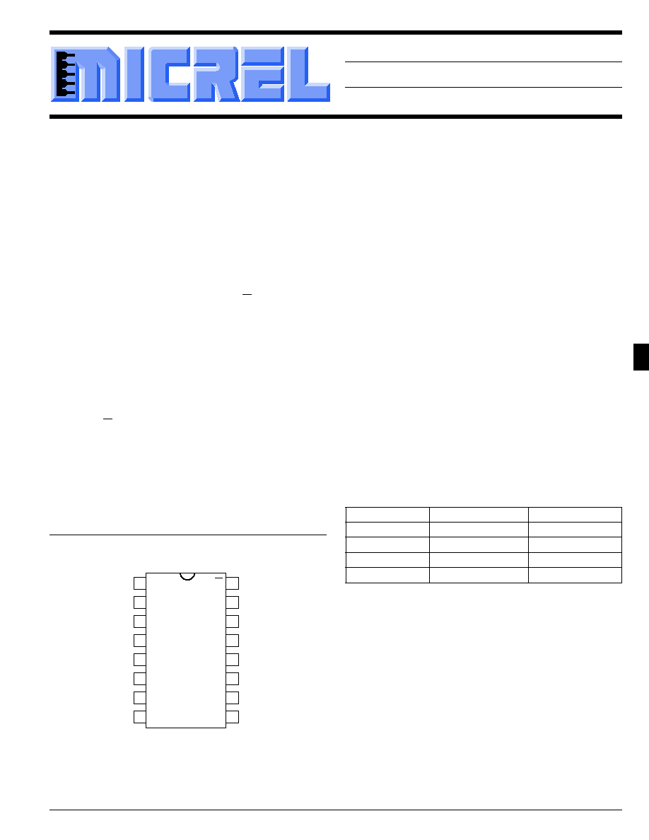
Pin Configuration
1
14
2
3
4
5
6
7
13
12
10
9
11
GND
C
T
Q
V
DD
5V REF
EA ≠
EA +
EA OUT
R
T
SYNC
CMR
MDC/SS
SHDN
NC
PWM
Q
8
15
16
DIP (N) or Wide SOIC (WM)
MIC3832/3833
Micrel
4-136
April 1998
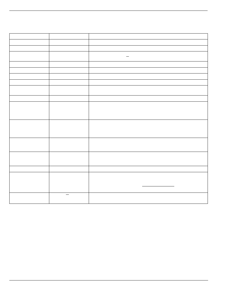
Pin Description
Pin Number
Pin Name
Pin Function
1
GND
Ground: Use as single-point ground tie point.
2
PWM
PWM Output: Variable duty-cycle totem pole output.
3
Q
Switch (Output): Totem pole output. Noninverting 50% duty cycle output
(180
∞
out-of-phase with Q with no dead time).
4
V
DD
Supply Voltage (Input): Clamped to 22V by internal zener diode.
5
5V REF
5V Bandgap Reference (Output)
6
EA ≠
Inverting Error Amplifier Input
7
EA +
Noninverting Error Amplifier Input
8
EA OUT
Error Amplifier Output: Connect to the appropriate feedback network to
adjust the open loop gain or frequency response.
9
NC
No Connection: Do not use--leave open.
10
SHDN
Overcurrent Shutdown (Input): >1 V disables outputs, >1.25V initiates soft-
start restart. For cycle-by-cycle current limiting, even in voltage-mode control
applications, connect to current sensor. If current sense is not used, connect
to GND.
11
MDC/SS
Maximum Duty Cycle/Soft Start (Input): Apply a dc voltage to adjust maxi-
mum duty cycle (see chart). Adjust soft start by adding capacitance to
increase turn-on time during initial start up or restart after overcurrent
shutdown.
12
CMR
Current Mode Ramp: Feed point for a sample of inductor current when using
current mode control. For voltage-mode control, connect directly to the C
T
pin.
13
SYNC
Synchronization (Input): AC coupled input from an external master clock
(reference) signal. If not used, leave unconnected. A high (>1.5V) resets the
C
T
ramp.
14
R
T
Oscillator Timing Resistor: Connect 4k
minimum resistor to GND.
15
C
T
Oscillator Timing Capacitor: Connect capacitor to GND. See "Typical
Characteristics: Discharge Time" graph for capacitor value.
Maximum oscillator frequency
1
2
discharge
time
=
◊
(
)
16
Q
Switch (Output): Totem pole output. Inverting 50% duty cycle output (180
∞
out-of-phase with Q with no deadtime).
April 1998
4-137
MIC3832/3833
Micrel
4
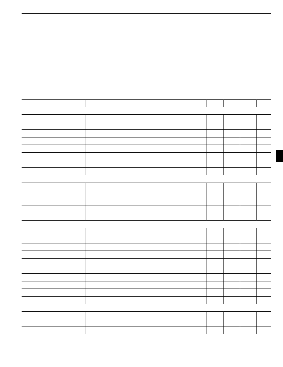
Electrical Characteristics
(Notes 2, 3)
T
A
= ≠40
∞
C to +85
∞
C, V
DD
= 15V, f = 52kHz unless otherwise specified.
Parameter
Conditions
Min
Typical
Max
Units
Reference Section
Output Voltage
I
o
= 1mA, T
A
= 25
∞
C
4.90
5.0
5.10
V
Input Regulation
V
CC
= 12V to 20V
5
20
mV
Output Regulation
I
O
= 1mA to 20mA
6
25
mV
Temperature Stability
≠0.2
mV/
∞
C
Total Output Variation
50
mV
Output Noise Voltage
f = 10Hz to 10kHz, T
A
= 25
∞
C
50
µ
V
Long Term Stability
T
A
= 125
∞
C, 1000hrs.
5.0
mV
Output Short Circuit Current
V
REF
= 0
25
60
160
mA
Oscillator Section
Frequency
T
A
= 25
∞
C, R
T
= 16k
, C
T
= 2.2nF
47
52
57
kHz
Voltage Stability
V
CC
= 12V to 20V
0.5
%
Amplitude (C
t
)
1.7
V
P-P
Discharge Current
T
A
= 25
∞
C
1
2.3
5
mA
Synchronization
ac coupled
1.5
V
Error Amplifier Section
Input Offset Voltage
≠15
±
2
15
mV
Input Bias Current
0.6
3.0
µ
A
Input Offset Current
0.1
1.0
µ
A
Open Loop Gain
1V < V
O
< 4V
60
82
dB
CMRR
1.5V < V
CM
< 4.5V
75
95
dB
PSRR
12V < V
DD
< 20V
85
120
dB
Output Sink Current
V
EA OUT
= 1V
1.0
2.5
mA
Output Source Current
V
EA OUT
= 4V
≠0.5
≠1.3
mA
Output High Voltage
I
EA OUT
= ≠0.5mA
4.0
4.9
5.0
V
Output Low Voltage
I
EA OUT
= 1mA
0.6
1.0
V
Soft Start/Max Duty Cycle Section
Bias Current
≠0.05
µ
A
Discharge Current
1
3
mA
Duty Cycle Clamp Accuracy
40
50
60
%
Operating Ratings
Storage Temperature Range ................... ≠65
∞
C to +150
∞
C
Operating Temperature Range .................. ≠40
∞
C to +85
∞
C
Reference Load Current ............................................. 25mA
Supply Voltage (V
DD
): MIC3832 ....................... 16V to 21V
Supply Voltage (V
DD
): MIC3833 ...................... 7.6V to 21V
Oscillator Frequency Range ..................... 10kHz to 500kHz
Oscillator Timing Resistor ............................. 3k
to 100k
Oscillator Timing Capacitor .............................. 1nF to 10nF
Absolute Maximum Ratings
(Note 1)
Supply Voltage, V
DD
(continuous) ................................. 22V
Source/Sink Load Current (peak) .................................... 1A
Maximum Supply (Zener) Current .............................. 50mA
Junction Temperature ............................................... 150
∞
C
Lead Temperature, Soldering ....................... 260
∞
C for 10s
JA
Plastic DIP ....................................................... 130
∞
C/W
MIC3832/3833
Micrel
4-138
April 1998
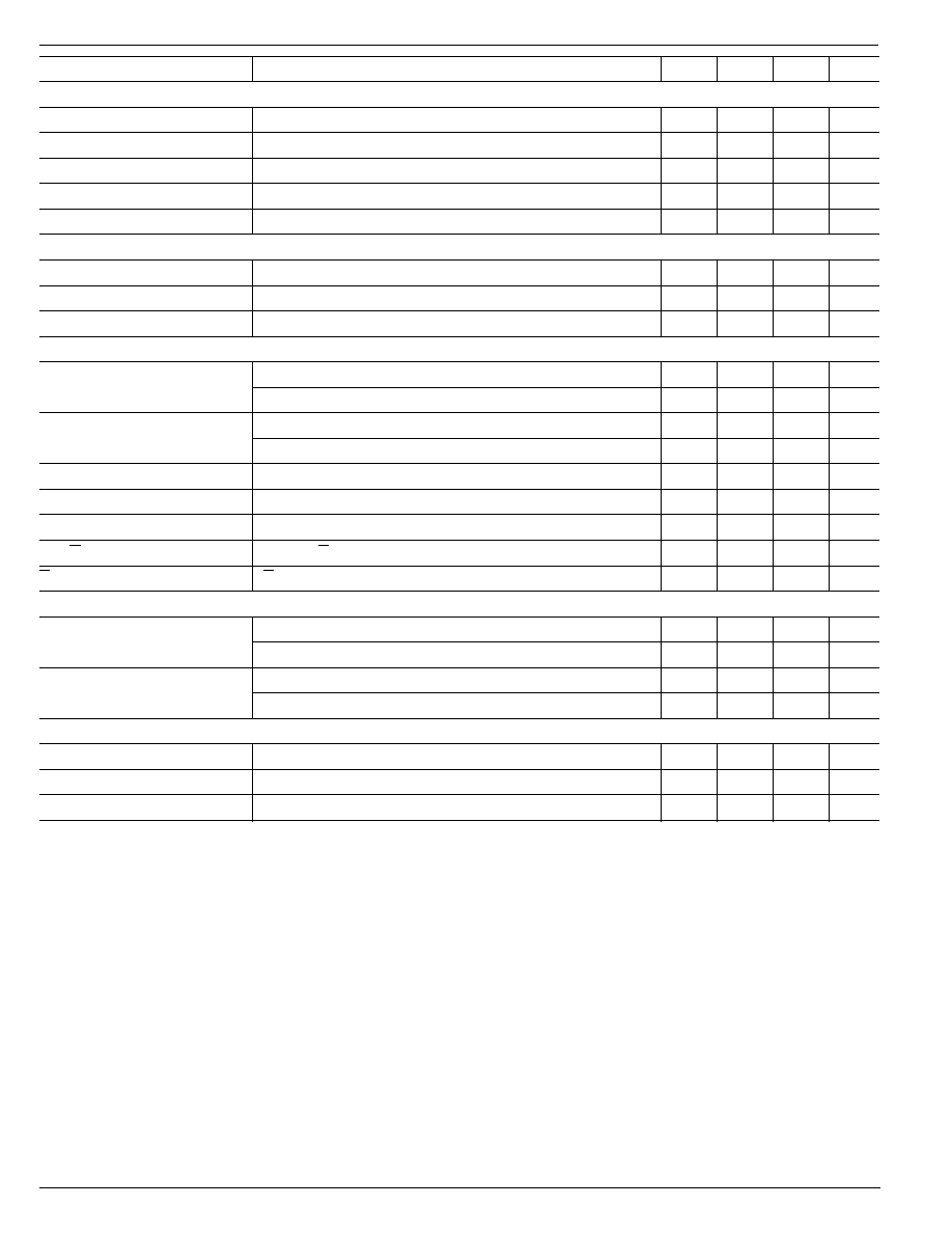
Parameter
Conditions
Min
Typical
Max
Units
Current Limit/Shutdown Section
Bias Current
≠0.02
µ
A
Current Limit Threshold
0.9
1.0
1.1
V
Shutdown Threshold
1.125
1.25
1.375
V
Delay to Output
400
600
ns
Front Edge Blanking Time
140
ns
PWM Comparator Section
Bias Current
measured at CMR (pin 12)
≠2
≠0.05
2
µ
A
Duty Cycle Range
C = 2.2nF
0
85
%
Delay to Output
300
500
ns
Output Sections
Output Low Level
I
SINK
= 20mA
0.1
0.4
V
I
SINK
= 200mA
1.5
2.5
V
Output High Level
I
SOURCE
= 20mA
12.5
V
I
SOURCE
= 200mA
12
13.1
V
Rise Time
C
L
= 1000pF
50
150
ns
Fall Time
C
L
= 1000pF
50
150
ns
UVLO Saturation
I
SINK
= 1mA
0.7
1.1
V
Q to Q Overlap
Q rising, Q falling, 50%
50
ns
Q to Q Overlap
Q rising, Q falling, 50%
50
ns
Undervoltage Lockout Section
Upper Threshold--Startup
MIC3832
15.9
V
MIC3833
8.3
V
Lower Threshold--Operating
MIC3832
9.8
V
(Shutdown)
MIC3833
7.8
V
Total Standby Current
Startup Current
0.04
0.2
mA
Operating Supply
17
mA
V
CC
Zener Voltage
I
CC
= 25mA
22
V
Note 1
Absolute Maximum Ratings indicate limits beyond which damage to the device may occur. Electrical specifications do not apply when
operating the device beyond its specified Operating Ratings.
Note 2
Minimum and maximum Electrical Characteristics are 100% tested at T
A
= 25
∞
C and T
A
= 85
∞
C, and 100% guaranteed over the entire range.
Typicals are characterized at 25
∞
C and represent the most likely parametric norm.
Note 3
All pins ESD protected to 2kV. Test conditions: Supply pin grounded; all other pins floating.

April 1998
4-139
MIC3832/3833
Micrel
4
Typical Characteristics
4.94
4.96
4.98
5.00
5.02
5.04
5.06
-40
0
40
80
120
160
REFERENCE VOLTAGE (V)
JUNCTION TEMPERATURE (
∞
C)
Reference Voltage vs.
Junction Temperature
15.6
15.8
16.0
16.2
16.4
-40
0
40
80
120
160
UNDER-VOLTAGE LOCKOUT (V) 9.2
9.4
9.6
9.8
10.0
-40
0
40
80
120
160
JUNCTION TEMPERATURE (
∞
C)
MIC3832 Undervoltage
Lockout vs. Junct. Temp.
ON
OFF
10
100
1000
1
10
100
FREQUENCY (Hz)
TIMING RESISTANCE (k
)
Oscillator Frequency
vs. Timing Resistance
85pF
550pF
1.1nF
2.2nF
10.2nF
Note 4
0.1
1
10
1
10
TIMING CAPACITOR DISCHARGE TIME (
µ
s)
TIMING CAPACITOR (nF)
Discharge Time vs.
Timing Capacitance
-40
∞
C
125
∞
C
25
∞
C
2
3
4
5 6
8
0
1
2
3
4
5
-40
0
40
80
120
160
DISCHARGE CURRENT (mA)
JUNCTION TEMPERATURE (
∞
C)
Oscillator Discharge
Current vs. Junct. Temp.
0
10
20
30
40
50
60
70
80
90
100
0
1
2
3
4
5
MAXIMUM DUTY CYCLE (%)
MDC CONTROL VOLTAGE (V)
Voltage-Mode Max. Duty
Cycle vs. MDC Voltage
Note 5
0
1
2
3
4
5
0
0.2
0.4
0.6
0.8
1
OUTPUT SATURATION VOLTAGE (V)
OUTPUT SINK CURRENT (A)
Output Saturation Voltage
vs. Output Sink Current
-55
∞
C
125
∞
C
25
∞
C
0
1
2
3
0
1
2
3
4
5
6
CURRENT SENSE THRESHOLD (V)
ERROR AMP OUTPUT (V)
Current Sense Threshold
vs. Error Amplifier Output
25
∞
C
125
∞
C
-55
∞
C
V
II
= 1
V
II
= 3
V
II
= 2
-25
0
25
50
75
100
-180
-135
-90
-45
0
45
1x10
1
1x10
2
1x10
3
1x10
4
1x10
5
1x10
6
1x10
7
1x10
8
AMPLITUDE (dB)
PHASE (
∞
)
FREQUENCY (Hz)
AMPLITUDE
PHASE
Error Amplifier Open-Loop
Frequency Response
7.0
7.5
8.0
8.5
9.0
-40
0
40
80
120
160
REFERENCE VOLTAGE (V)
JUNCTION TEMPERATURE (
∞
C)
MIC3833 Undervoltage
Lockout vs. Junct. Temp.
ON
OFF
0
1
2
3
4
5
0
0.2
0.4
0.6
0.8
1
OUTPUT VOLTAGE DROP (V)
OUTPUT SOURCE CURRENT (A)
Output Voltage Drop vs.
Output Source Current
125
∞
C
25
∞
C
-55
∞
C
Note 4:
CMR (pin 12) connected to C
T
(pin 15).
Note 5:
CMR (pin 12) connected to C
T
(pin 15). MDC voltage measured
at MDC/SS (pin 11).
C
T
= 1nF, R
T
= 10k
.