 | –≠–ª–µ–∫—Ç—Ä–æ–Ω–Ω—ã–π –∫–æ–º–ø–æ–Ω–µ–Ω—Ç: MIC3839 | –°–∫–∞—á–∞—Ç—å:  PDF PDF  ZIP ZIP |
August 2003
1
MIC3838/3839
MIC3838/3839
Micrel
MIC3838/3839
Flexible Push-Pull PWM Controller
General Description
The MIC3838 and MIC3839 are a family of complementary
output push-pull PWM control ICs that feature high speed and
low power consumption. The MIC3838/9 are ideal for telecom
level (36V to 75V) isolated step down dc/dc conversion
applications where high output current, small size, and high
efficiency are required
The MIC3838/9 are designed for high flexibility with minimum
pin-count. The devices are easily configurable for either
voltage-mode or current-mode control. Additionally, the
MIC3838/9 can easily implement a volt-second clamp that
automatically limits the duty cycle during input transients,
allowing designers to use the smallest possible transformers
and power components. A 3V reference output is also avail-
able that eliminates the need for an external reference.
The dual-ended push-pull architecture of the MIC3838/9
allows more efficient utilization of the transformer than single-
ended topologies, allowing smaller size dc/dc solutions.
Additionally, the out-of-phase push-pull topology allows a
higher effective duty cycle, reducing input and output ripple
as well as stress on the external components. The dead-time
between the two outputs is adjustable between 60ns to
200ns, limiting the duty cycle of each output stage to less than
50%.
The MIC3838 has a turn-on threshold of 12.5V whereas the
MIC3839 has a lower turn-on threshold of 4.3V. Both devices
are available in a small size MSOP-10 package with an
operating range of ≠40
∞C to +85∞C.
Data sheets and support documentation can be found on
Micrel's web site at www.micrel.com.
Features
∑ Dual output drive stages in push-pull configuration
∑ Configurable for current-mode or voltage-mode control
∑ Easily implements volt-second clamp
∑ Leading edge current-sense blanking
∑ 3V reference output available
∑ 130
µA typical start-up current
∑ 1mA typical run current
∑ Operation to 1MHz
∑ On-chip error amplifier with 4MHz gain bandwidth
product
∑ Internal soft start
∑ On-chip V
DD
clamping
∑ Output drive stages capable of 500mA peak source
current, 1A peak sink current
Applications
∑ High efficiency "brick" power supply modules
∑ Half bridge converters
∑ Full bridge converters
∑ Push-pull converters
∑ Voltage-fed push-pull converters
∑ Telecom equipment and power supplies
∑ Industrial power supplies
∑ 42V automotive power supplies
∑ Base stations
∑ Networking power supplies
Micrel, Inc. ∑ 1849 Fortune Drive ∑ San Jose, CA 95131 ∑ USA ∑ tel + 1 (408) 944-0800 ∑ fax + 1 (408) 944-0970 ∑ http://www.micrel.com
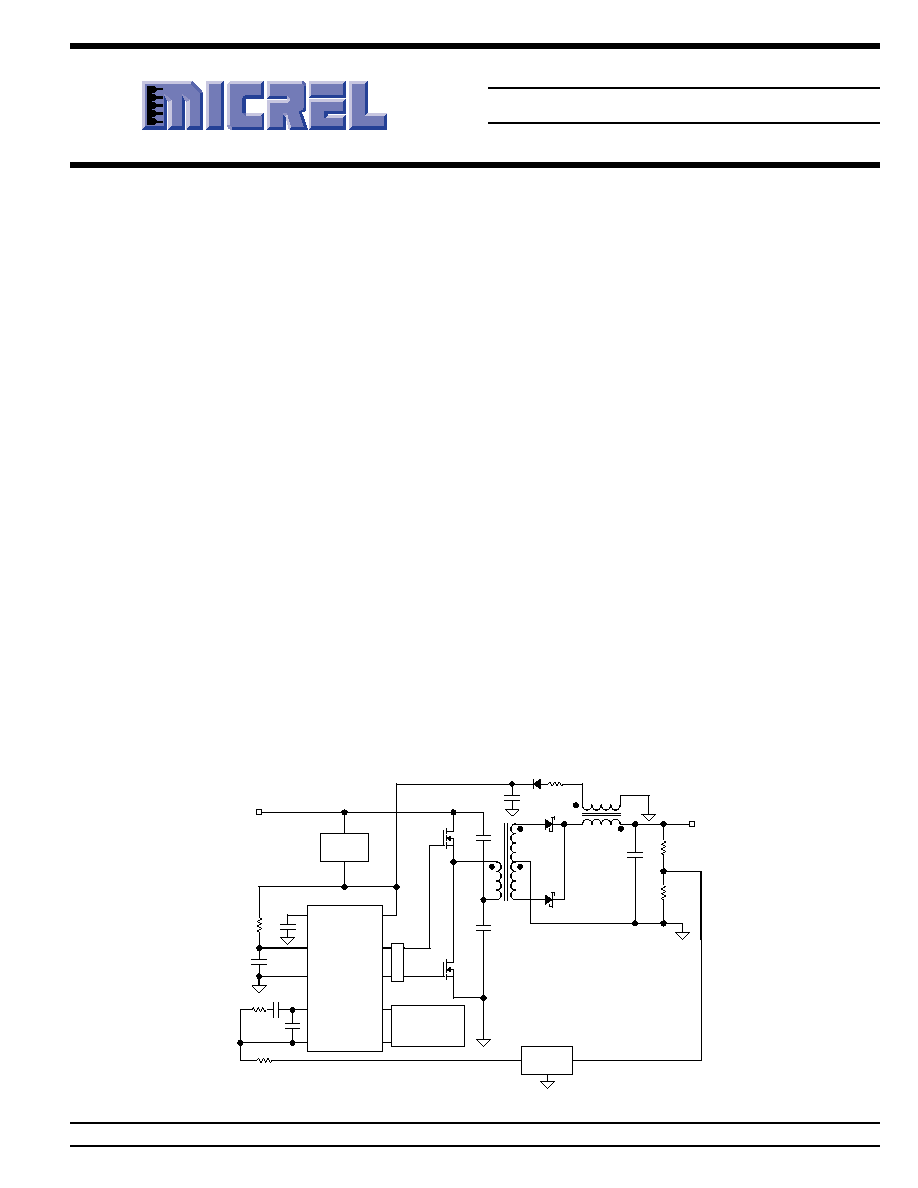
Typical Application
MIC3838x-x
V
OUT
12V 100W
VREF
RC
VDD
OUTA
COMP
GND
OUTB
RAMP
FB
ILIM
Start-Up
Circuitry
Driver
Reference
& Isolation
Feed Forward
Ramp/
Volt Sec Clamp
V
IN
36V to 75V
Voltage-Mode Half-Bridge Converter CIrcuit
MIC3838/3839
Micrel
MIC3838/3839
2
August 2003
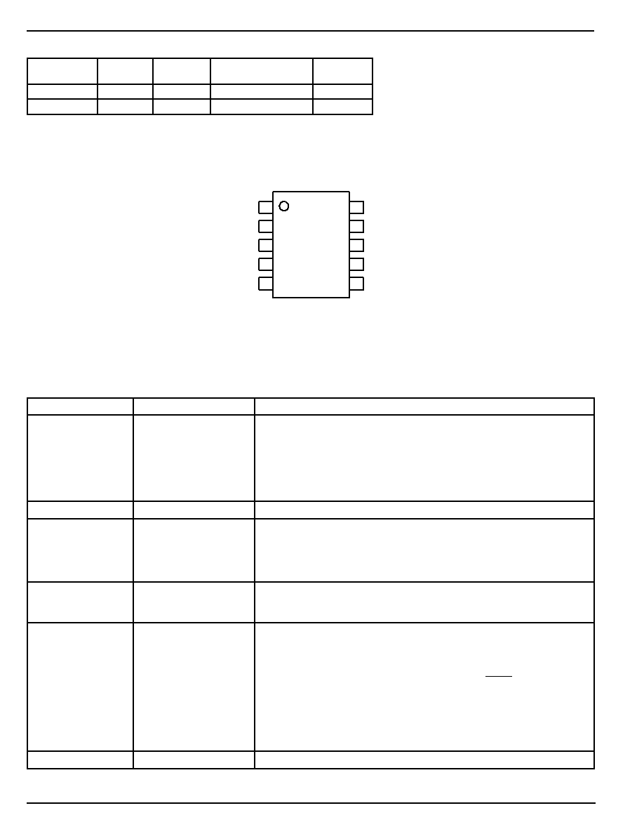
Ordering Information
Turn On
Turn Off
Part Number
Threshold
Threshold
Temperature Range
Package
MIC3838BMM
12.5V
8.3V
≠40
∞C to +85∞C
MSOP-10
MIC3839BMM
4.3V
4.1V
≠40
∞C to +85∞C
MSOP-10
Pin Configuration
1
COMP
FB
ILIM
RAMP
10 VREF
VDD
OUTA
OUTB
9
8
7
2
3
4
RC
GND
6
5
MSOP-10 (MM)
Pin Description
Pin Number
Pin Name
Pin Function
1
COMP
COMP is the output of the error amplifier and the input of the PWM
comparator. The error amplifier in the MIC3838 is a true low-output imped-
ance, 4MHz operational amplifier. As such, the COMP pin can both source
and sink current. However, the error amplifier is internally current limited, so
that zero duty cycle can be externally forced by pulling COMP to GND.
The MIC3838 family features built-in full cycle soft start. Soft start is imple-
mented as a clamp on the maximum COMP voltage.
2
FB
The inverting input to the error amplifier.
3
ILIM
The input to the peak current, and overcurrent comparators. The
overcurrent comparator is only intended for fault sensing. Exceeding the
overcurrent threshold will cause a soft start cycle. An internal MOSFET
discharges the current sense filter capacitor to improve dynamic perfor-
mance of the power converter.
4
RAMP
Input to the PWM comparator. Sawtooth ramp for PWM control. Allows for
either current-mode or voltage-mode control. An internal MOSFET dis-
charges the current sense filter capacitor.
5
RC
The oscillator programming pin. Only two components are required to
program the oscillator, a resistor (tied between V
DD
and RC), and a capaci-
tor (tied between RC and GND). The approximate oscillator frequency is
determined by the simple formula:
F
1.41
R C
OSCILLATOR
=
◊
The recommended range of timing resistors is between 7k
and 200k and
range of timing capacitors is between 100pF and 1000pF. Timing resistors
less than 7k
should be avoided. For best performance, keep the leads
between components as short as possible. Separate ground and VDD
traces to the external timing network are encouraged.
6
GND
Ground. Return path for signal and gate drive functions.

August 2003
3
MIC3838/3839
MIC3838/3839
Micrel
Pin Description
Pin Number
Pin Name
Pin Function
7, 8
OUTB, OUTA
Alternating high current output stages. Both stages are capable of driving
the gate of a power MOSFET. Each stage is capable of 500mA peak source
current, and 1A peak sink current.
The output stages switch at half the oscillator frequency, in a push/pull
configuration. When the voltage on the RC pin is rising, one of the two
outputs is high, but during fall time, both outputs are off. This "dead time"
between the two outputs, along with a slower output rise time than fall time,
insures that the two outputs can not be on at the same time. This dead time
is typically 60ns to 200ns and depends upon the values of the timing
capacitor and resistor.
The high-current output drivers consist of MOSFET output devices, which
switch from V
DD
to GND. Each output stage also provides a very low
impedance to overshoot and undershoot. This means that in many cases,
external Schottky clamp diodes are not required.
9
VDD
The power input connection for this device. Total V
DD
current is the sum of
quiescent V
DD
current and the average gate drive (OUT) current. Knowing
the operating frequency and the MOSFET gate charge (Qg), average OUT
current can be calculated from IOUT = Qg ∑ F, where Qg is the total gate
change of all MOSFETs (OUTA and OUTB) and F is oscillator switching
frequency. To prevent noise problems, bypass VDD to GND with a ceramic
capacitor as close to the chip as possible. A 1
µF decoupling capacitor is
recommended.
10
VREF
Internal 3V supply. Will source 1mA maximum.

MIC3838/3839
Micrel
MIC3838/3839
4
August 2003
Electrical Characteristics
(Note 5)
T
A
= T
J
= ≠40
∞C to +85∞C, V
DD
=10V, Note 10,1
µF capacitor from V
DD
to GND, R=22k
, C=330pF.
Parameter
Condition
Min
Typ
Max
Units
Internal Reference Section
Output voltage
I
OUT
= 0mA
2.85
3.0
3.15
V
Line Regulation
MIC3838 9V
V
DD
12V
2
10
mV
MIC3839 5V
V
DD
12V
Load Regulation
I
OUT
= 1mA
14
30
mV
Oscillator Section
Oscillator Frequency
180
200
220
kHz
Oscillator Amplitude/V
DD
Note 6
0.44
0.5
0.56
V/V
DD
Error Amp Section
Input Voltage
COMP = 2V
1.95
2
2.05
V
Input Bias Current
≠1
1
µA
Open Loop Voltage Gain
(Guaranteed by design)
60
80
dB
COMP Sink Current
FB = 2.2V, COMP = 1V
0.3
2.5
mA
COMP Source Current
FB = 1.3V, COMP = 3V, Note 7
≠0.15
≠0.5
mA
COMP PM Clamp Voltage
V
FB
= 0V
3.1
3.6
4.0
V
PWM Section
Maximum Duty Cycle
Measured at OUTA or OUTB
48
49
50
%
Minimum Duty Cycle
COMP = 0V
0
%
Current Sense Section
Gain
Guaranteed by design, Note 8
1.9
2.2
2.5
V/V
I
LIM
Maximum Input Signal
Note 9
0.45
0.5
0.55
V
I
LIM
to Output Delay
COMP = 3V, I
LIM
from 0mV to 600mV
70
200
ns
Ramp or I
LIM
Source Current
≠200
nA
Ramp or I
LIM
Sink Current
Ramp = I
LIM
= 0.5V, RC = 5.5V Note 10
5
10
mA
I
LIM
Over Current Threshold
0.7
0.75
0.8
V
COMP to Ramp Offset
Ramp = I
LIM
= 0V
0.35
0.8
1.2
V
Output Section
OUT Low Level
I = 100mA
0.5
1
V
OUT High Level
I = ≠50mA, V
DD
≠ OUT
0.5
1
V
Rise Time
C
L
= 1nF
25
60
ns
Fall Time
C
L
= 1nF
25
60
ns
Absolute Maximum Rating
(Note 1)
Supply Voltage (I
DD
10mA) ...................................... +15V
Supply Current ........................................................... 20mA
OUTA/OUTB Source Current (peak) ...................... ≠0.5A
OUTA/OUTB Sink Current (peak) ............................ 1.0A
COMP Pin .................................................................... V
DD
Analog Inputs (FB, ILIM, RAMP) ......... ≠0.3V to V
DD
+0.3V
NOT TO EXCEED 6V
Junction Temperature .............................. ≠55
∞C to +150∞C
Storage Temperature (T
S
) ....................... ≠65
∞C to +150∞C
Lead Temperature (soldering, 10 sec.) ................... +300
∞C
ESD Rating, Note 3 ...................................................... 2kV
Operating Ratings
(Note 2)
V
DD
Input Voltage (V
DD
) .......................................... Note 4
Oscillator Frequency (f
OSC
) ....................... 10kHz to 1MHz
Ambient Temperature (T
A
) ......................... ≠40
∞C to +85∞C
Package Thermal Resistance
MSOP-10 (
JA
) .................................................. 115
∞C/W
August 2003
5
MIC3838/3839
MIC3838/3839
Micrel
Parameter
Condition
Min
Typ
Max
Units
Undervoltage Lockout Section
Start Threshold
MIC3838, Note 11
11.5
12.5
13.5
V
MIC3839
4.1
4.3
4.5
V
Minimum Operating Voltage
MIC3838
7.6
8.3
9
V
After Start
MIC3839
3.9
4.1
4.3
V
Hysteresis
MIC3838
3.5
4.2
5.1
V
MIC3839
0.1
0.2
0.3
V
Soft Start Section
COMP Rise Time
FB = 1.8V, Rise from 0.5V to 3V
2.5
20
ms
Overall Section
Startup Current
V
DD
< Start Threshold (MIC3839)
130
260
µA
Operating Supply Current
FB = 0V, Ramp = I
LIM
= 0V, Notes 11, 12
1.5
2
mA
V
DD
Zener Shunt Voltage
I
DD
= 10mA, Note 13
13
14
15
V
Note 1.
Exceeding the absolute maximum rating may damage the device.
Note 2.
The device is not guaranteed to function outside its operating rating.
Note 3.
Devices are ESD sensitive. Handling precautions recommended. Human body model, 1.5k in series with 100pF.
Note 4.
Maximum operating voltage is equal to the V
DD
(zener) shunt voltage. When operating at or near the shunt voltage, care must be taken to limit
the V
DD
pin current less than the 20mA V
DD
maximum current rating.
Note 5.
Specification for packaged product only.
Note 6.
Measured at RC.
Note 7.
COMP pin is internally clamped to 3.65V(typ.). COMP pin source current is measured at V
COMP
= 3.0V to avoid interferring with clamp.
Minimum source current is higher as V
COMP
approaches V
CLAMP
.
Note 8.
Gain is defined by A =
V
V
COMP
CS
, 0
V
CS
0.4V.
Note 9.
Parameter measured at trip point of latch with FB at 0V
Note 10. The internal current sink on the Ramp and I
LIM
pin are designed to discharge an external filter capacitor. It is not intended to be a DC sink
path. Internal discharge FET should be able to discharge the Volt-Sec clamp and feed-forward circuits in the figure below within 50ns.
Note 11. For MIC3838, set V
DD
above the start threshold before setting at 10V.
Note 12. Does not include current in the external oscillator network.
Note 13. Start threshold and Zener Shunt threshold track one another.