September 2000
1
MIC384
MIC384
Micrel
MIC384
Three-Zone Thermal Supervisor
Advance Information
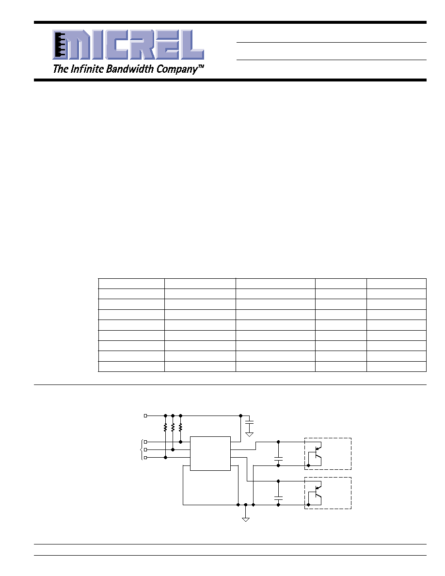
Typical Application
CLK
FROM
SERIAL BUS
HOST
REMOTE
DIODE
2200pF
0.1
µ
F
MIC384
/INT
GND
3.3V
DATA
3
◊
10k
pull-ups
VDD
T1
T2
A0
REMOTE
DIODE
2200pF
3-Channel SMBus Temperature Measurement System
Features
∑ Measures Local and Two Remote Temperatures
∑ 2-Wire SMBus-compatible Interface
∑ Programmable Thermostat Settings for All Three Zones
∑ Open-Drain Interrupt Output Pin
∑ Interrupt Mask and Status Bits
∑ Fault Queues to Prevent Nuisance Tripping
∑ Low Power Shutdown Mode
∑ Failsafe response to diode faults
∑ 2.7V to 5.5V Power Supply Range
∑ 8-Lead SOIC and MSOP Packages
Applications
∑ Desktop, Server and Notebook Computers
∑ Power Supplies
∑ Test and Measurement Equipment
∑ Wireless Systems
∑ Networking/Datacom Hardware
Micrel, Inc. ∑ 1849 Fortune Drive ∑ San Jose, CA 95131 ∑ USA ∑ tel + 1 (408) 944-0800 ∑ fax + 1 (408) 944-0970 ∑ http://www.micrel.com
General Description
The MIC384 is a versatile digital thermal supervisor capable
of measuring temperature using its own internal sensor and
two inexpensive external sensors or embedded silicon di-
odes such as those found in the Intel Pentium III* CPU. A 2-
wire serial interface is provided to allow communication with
either I
2
C** or SMBus* masters. The open-drain interrupt
output pin can be used as either an over-temperature alarm
or a thermostatic control signal.
Interrupt mask and status bits are provided for reduced
software overhead. Fault queues prevent nuisance tripping
due to thermal or electrical noise. A programmable address
pin permits two devices to share the bus. (Alternate base
addresses available ≠ contact Micrel.) Superior perfor-
mance, low power and small size makes the MIC384 an
excellent choice for multiple zone thermal management
applications.
*SMBus and Pentium III are trademarks of Intel Corporation.
**I
2
C is a trademark of Philips Electronics, N.V.
Ordering Information
Part Number
Base Address
(
*
)
Junction Temp. Range
Package
Notes
MIC384-0BM
100 100x
≠55
∞
C to +125
∞
C
8-Lead SOP
MIC384-1BM
100 101x
≠55
∞
C to +125
∞
C
8-Lead SOP
Contact Factory
MIC384-2BM
100 110x
≠55
∞
C to +125
∞
C
8-Lead SOP
Contact Factory
MIC384-3BM
100 111x
≠55
∞
C to +125
∞
C
8-Lead SOP
Contact Factory
MIC384-0BMM
100 100x
≠55
∞
C to +125
∞
C
8-Lead MSOP
MIC384-1BMM
100 101x
≠55
∞
C to +125
∞
C
8-Lead MSOP
Contact Factory
MIC384-2BMM
100 110x
≠55
∞
C to +125
∞
C
8-Lead MSOP
Contact Factory
MIC384-3BMM
100 111x
≠55
∞
C to +125
∞
C
8-Lead MSOP
Contact Factory
* The least-significant bit of the slave address is determined by the state of the A0 pin.
MIC384
Micrel
MIC384
2
September 2000
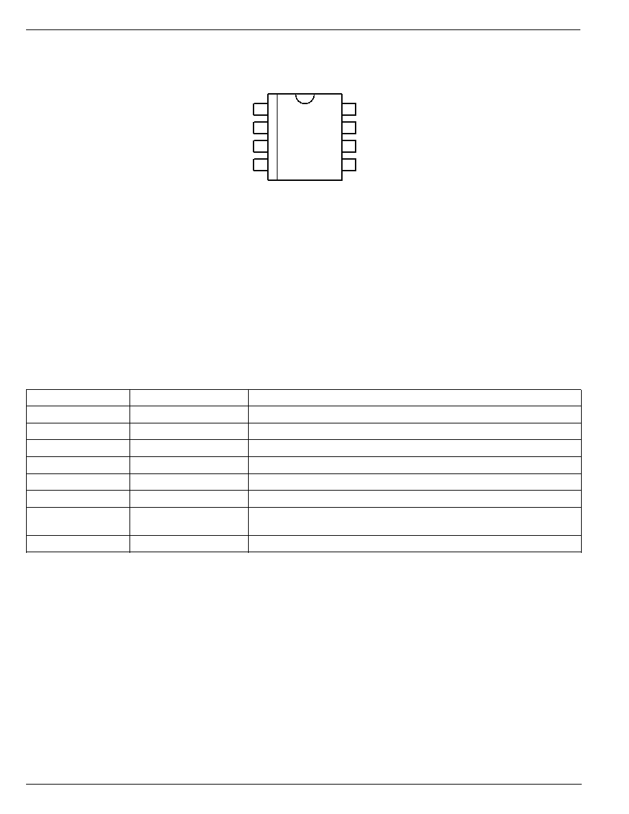
Pin Description
Pin Number
Pin Name
Pin Function
1
DATA
Digital I/O: Open-drain. Serial data input/output.
2
CLK
Digital Input: The host provides the serial bit clock on this input.
3
/INT
Digital Output: Open-drain. Interrupt or thermostat output.
4
GND
Ground: Power and signal return for all IC functions.
5
T2
Analog Input: Connection to remote temperature sensor (diode junction)
6
T1
Analog Input: Connection to remote temperature sensor (diode junction)
7
A0
Digital Input: Slave address selection input. See Table 1. MIC284 Slave
Address Setings.
8
VDD
Analog Input: Power supply input to the IC.
Pin Configuration
1
DATA
CLK
/INT
GND
8
VDD
A0
T1
T2
7
6
5
2
3
4

September 2000
3
MIC384
MIC384
Micrel
Absolute Maximum Ratings
(Note 1)
Power Supply Voltage, V
DD ...................................................
6.0V
Voltage on Any Pin ................................ ≠0.3V to V
DD
+0.3V
Current Into Any Pin .................................................
±
10mA
Power Dissipation, T
A
= +125
∞
C ............................... 30mW
Junction Temperature ............................................. +150
∞
C
Storage Temperature ............................... ≠65
∞
C to +150
∞
C
ESD Ratings (Note 3)
Human Body Model .................................................. TBD V
Machine Model ......................................................... TBD V
Soldering
Vapor Phase (60 sec.) ............................. +220
∞
C
+5
/
≠0
∞
C
Infrared (15 sec.) ...................................... +235
∞
C
+5
/
≠0
∞
C
Operating Ratings
(Note 2)
Power Supply Voltage, V
DD ..............................
+2.7V to +5.5V
Ambient Temperature Range (T
A
) ............ -55
∞
C to +125
∞
C
Package Thermal Resistance (
JA
)
SOP ................................................................. +152
∞
C/W
MSOP .............................................................. +206
∞
C/W
Electrical Characteristics
2.7V
V
DD
5.5; T
A
= +25
∞
C, bold values indicate ≠55
∞
C
T
A
+125
∞
C, Note 4; unless noted.
Symbol
Parameter
Condition
Min
Typ
Max
Units
Power Supply
I
DD
Supply Current
/INT, open, A0 = V
DD
or GND,
350
750
µ
A
CLK = DATA = high, normal mode
/INT, open, A0 = V
DD
or GND,
3
µ
A
shutdown mode, CLK = 100kHz
/INT, open, A0 = V
DD
or GND,
1
10
µ
A
shutdown mode, CLK = DATA = high
t
POR
Power-On Reset Time; Note 7
V
DD
> V
POR
200
µ
s
V
POR
Power-On Reset Voltage
all registers reset to default values,
2.0
2.7
V
A/D conversions initiated
V
HYST
Power-On Reset Hysteresis Voltage
250
mV
Temperature-to-Digital Converter Characteristics
Accuracy--Local Temperature
0
∞
C
T
A
+100
∞
C, /INT open,
±
1
±
2
∞
C
Note 4, 9
3V
V
DD
3.6V
≠55
∞
C
T
A
+125
∞
C, /INT open,
±
2
±
3
∞
C
3V
V
DD
3.6V
Accuracy--Remote Temperature
0
∞
C
T
D
+100
∞
C, /INT open,
±
1
±
3
∞
C
Note 5, 4, 9
3V
V
DD
3.6V, 0
∞
C
T
A
+85
∞
C
≠55
∞
C
T
D
+125
∞
C, /INT open,
±
2
±
5
∞
C
3V
V
DD
3.6V, 0
∞
C
T
A
+85
∞
C
t
CONV0
Conversion Time, local zone
50
80
ms
Note 7, 8
t
CONV1
Conversion Time, remote zone
Note 7, 8
100
160
ms
Remote Temperature Inputs (T1, T2)
I
F
Current to External Diode
high level, T1 or T2 forced to 1.5V
224
400
µ
A
Note 7
low level
7.5
14
µ
A
Address Input (A0)
V
IL
Low Input Voltage
2.7V
V
DD
5.5V
0.6
V
V
IH
High Input Voltage
2.7V
V
DD
5.5V
2.0
V
C
IN
Input Capacitance
10
pF
I
LEAK
Input Current
±
0.01
±
1
µ
A

MIC384
Micrel
MIC384
4
September 2000
Symbol
Parameter
Condition
Min
Typ
Max
Units
Serial Data I/O Pin (DATA)
V
OL
Low Output Voltage
I
OL
= 3mA
0.4
V
Note 6
I
OL
= 6mA
0.8
V
V
IL
Low Input Voltage
2.7V
V
DD
5.5V
0.3V
DD
V
V
IH
High Input Voltage
2.7V
V
DD
5.5V
0.7V
DD
V
C
IN
Input Capacitance
10
pF
I
LEAK
Input current
±
0.01
±
1
µ
A
Serial Clock Input (CLK)
V
IL
Low Input Voltage
2.7V
V
DD
5.5V
0.3V
DD
V
V
IH
High Input Voltage
2.7V
V
DD
5.5V
0.7V
DD
V
C
IN
Input Capacitance
10
pF
I
LEAK
Input current
±
0.01
±
1
µ
A
Status Output (/INT)
V
OL
Low Output Voltage,
I
OL
= 3mA
0.4
V
Note 6
I
OL
= 6mA
0.8
V
t
INT
Interrupt Propagation Delay,
from TEMPx > T_SETx or TEMPx < T_HYSTx
t
CONV
+1
µ
s
Note 7, 8
to /INT < V
OL
, FQ = 00, R
PULLUP
= 10k
t
nINT
Interrupt Reset Propagation Delay,
from any register read to /INT > V
OH
,
1
µ
s
Note 7
R
PULLUP
= 10k
T_SET0
Default T_SET0 Value
t
POR
after V
DD
> V
POR
81
81
81
∞
C
T_HYST0
Default T_HYST0 Value
t
POR
after V
DD
> V
POR
76
76
76
∞
C
T_SET1
Default T_SET1 Value
t
POR
after V
DD
> V
POR
97
97
97
∞
C
T_HYST1
Default T_HYST1 Value
t
POR
after V
DD
> V
POR
92
92
92
∞
C
T_SET2
Default T_SET2 Value
t
POR
after V
DD
> V
POR
97
97
97
∞
C
T_HYST2
Default T_HYST2 Value
t
POR
after V
DD
> V
POR
92
92
92
∞
C
Serial Interface Timing (Note 7)
t
1
CLK (Clock) Period
2.5
µ
s
t
2
Data In Setup Time to CLK High
100
ns
t
3
Data Out Stable After CLK Low
0
ns
t
4
DATA Low Setup Time to CLK Low
start condition
100
ns
t
5
DATA High Hold Time
stop condition
100
ns
After CLK High
Note 1.
Exceeding the absolute maximum rating may damage the device.
Note 2.
The device is not guaranteed to function outside its operating rating.
Note 3.
Devices are ESD sensitive. Handling precautions recommended.
Human body model: 1.5k in series with 100pF. Machine model: 200pF, no series resistance.
Note 4.
Final test on outgoing product is performed at T
A
= TBD
∞
C.
Note 5.
T
D
is the temperature of the remote diode junction. Testing is performed using a single unit of one of the transistors listed in Table 6.
Note 6.
Current into this pin will result in self-heating of the MIC384. Sink current should be minimized for best accuracy.
Note 7.
Guaranteed by design over the operating temperature range. Not 100% production tested.
Note 8.
t
CONV
= t
CONV0
+(2 X t
CONV1
). t
CONV0
is the conversion time for the local zone; t
CONV1
is the conversion time for the remote zones.`

September 2000
5
MIC384
MIC384
Micrel
Note 9.
Accuracy specification does not include quantization noise, which may be as great as
±
1
/
2
LSB (
±
0.5
∞
C).
Timing Diagram
t
1
t
2
t
5
t
4
t
3
SCL
SDA Data In
SDA Data Out
Serial Interface Timing