 | –≠–ª–µ–∫—Ç—Ä–æ–Ω–Ω—ã–π –∫–æ–º–ø–æ–Ω–µ–Ω—Ç: MIC38C44B | –°–∫–∞—á–∞—Ç—å:  PDF PDF  ZIP ZIP |
MIC38C42/3/4/5
Micrel
August 2000
1
MIC38C42/3/4/5
MIC38C42/3/4/5
BiCMOS Current-Mode PWM Controllers
General Description
The MIC38C4x are fixed frequency, high performance, cur-
rent-mode PWM controllers. Micrel's BiCMOS devices are
pin compatible with 384x bipolar devices but feature several
improvements.
Undervoltage lockout circuitry allows the '42 and '44 versions
to start up at 14.5V and operate down to 9V, and the '43 and
'45 versions start at 8.4V with operation down to 7.6V. All
versions operate up to 20V.
When compared to bipolar 384x devices operating from a
15V supply, start-up current has been reduced to 50
µA
typical and operating current has been reduced to 4.0 mA
typical. Decreased output rise and fall times drive larger
MOSFETs, and rail-to-rail output capability increases effi-
ciency, especially at lower supply voltages. The MIC38C4x
also features a trimmed oscillator discharge current and
bandgap reference.
MIC38C4x denotes 8-pin plastic DIP, SOIC, and MM8TM
packages. MIC38C4x-1 denotes 14-pin plastic DIP and
SOIC packages. 8-pin devices feature small size, while 14-
pin devices separate the analog and power connections for
improved performance and power dissipation.
For fast rise and fall times and higher output drive, refer to the
MIC38HC4x.
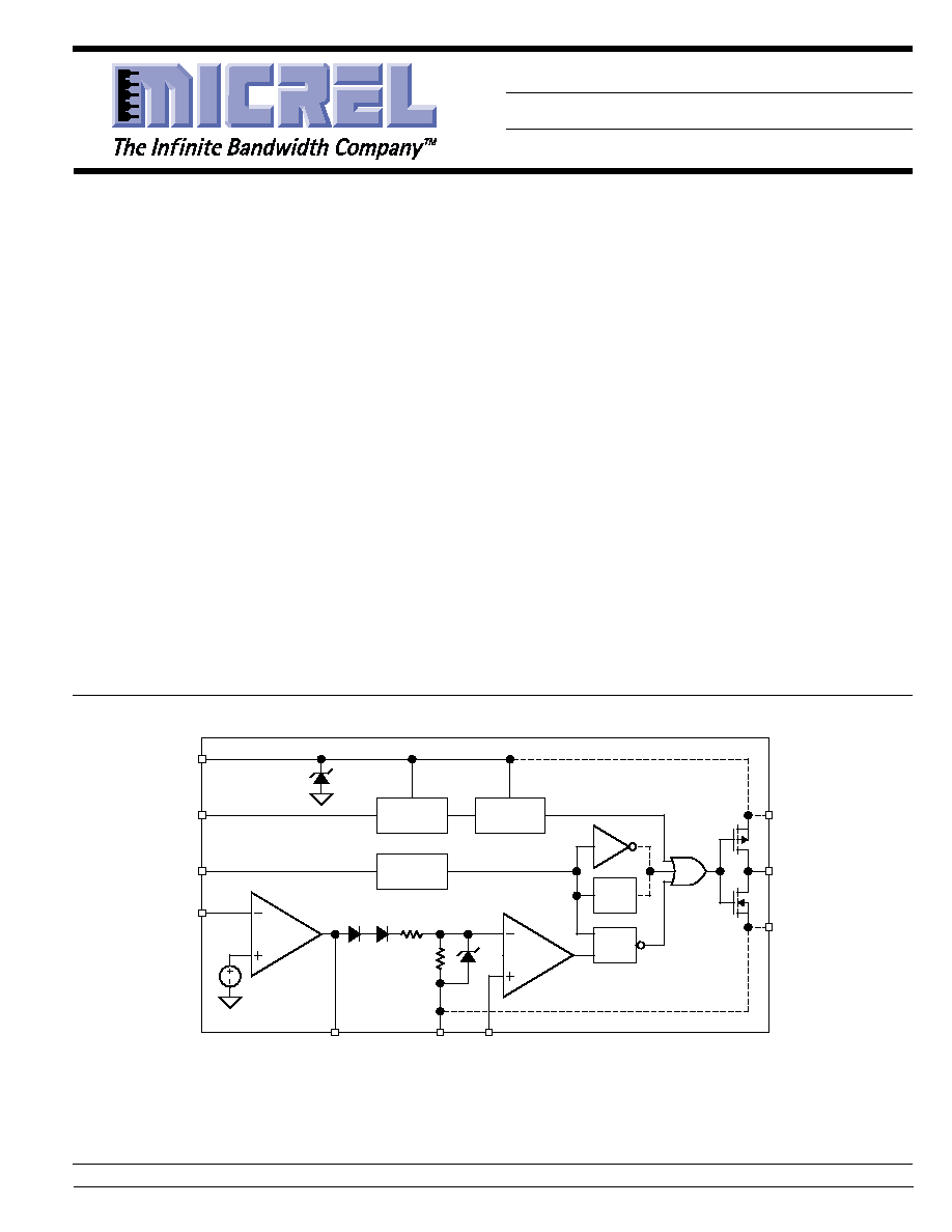
Functional Diagram
Features
∑ Fast 40ns output rise and 30ns output fall times
∑ ≠40
∞C to +85∞C temperature range
meets UC284x specifications
∑ High-performance, low-power BiCMOS Process
∑ Ultralow start-up current (50
µA typical)
∑ Low operating current (4mA typical)
∑ CMOS outputs with rail-to-rail swing
∑
500kHz current-mode operation
∑ Trimmed 5V bandgap reference
∑ Pin-for-pin compatible with UC3842/3843/3844/3845(A)
∑ Trimmed oscillator discharge current
∑ UVLO with hysteresis
∑ Low cross-conduction currents
Applications
∑ Current-mode, off-line, switched-mode power supplies
∑ Current-mode, dc-to-dc converters.
∑ Step-down "buck" regulators
∑ Step-up "boost" regulators
∑ Flyback, isolated regulators
∑ Forward converters
∑ Synchronous FET converters
T
Q
S
R
Q
R
2R
Oscillator
UVLO
5V
Reference
VDD
7 (12)
VREF
8 (14)
RT/CT
4 (7)
FB
2 (3)
2.5V
COMP
1 (1)
GND*(AGND)
5 (9)
ISNS
3 (5)
(VD)
(11)
OUT
6 (10)
(PGND)
(8)
( ) pins are on MIC38C4x-1 (14-lead) versions only
* MIC38C4x (8-lead) versions only
MIC38C42, MIC38C43 (96% max. duty cycle) versions only
MIC38C44, MIC38C45 (50% max. duty cycle) versions only
35V
*
*
MM8 is a trademark of Micrel, Inc.
Micrel, Inc. ∑ 1849 Fortune Drive ∑ San Jose, CA 95131 ∑ USA ∑ tel + 1 (408) 944-0800 ∑ fax + 1 (408) 944-0970 ∑ http://www.micrel.com
MIC38C42/3/4/5
Micrel
MIC38C42/3/4/5
2
August 2000
Ordering Information
Part Number
Temperature Range
Package
MIC38C42BN
≠40
∞C to +85∞C
8-pin Plastic DIP
MIC38C43BN
≠40
∞C to +85∞C
8-pin Plastic DIP
MIC38C44BN
≠40
∞C to +85∞C
8-pin Plastic DIP
MIC38C45BN
≠40
∞C to +85∞C
8-pin Plastic DIP
MIC38C42-1BN
≠40
∞C to +85∞C
14-pin Plastic DIP
MIC38C43-1BN
≠40
∞C to +85∞C
14-pin Plastic DIP
MIC38C44-1BN
≠40
∞C to +85∞C
14-pin Plastic DIP
MIC38C45-1BN
≠40
∞C to +85∞C
14-pin Plastic DIP
MIC38C42BM
≠40
∞C to +85∞C
8-pin SOIC
MIC38C43BM
≠40
∞C to +85∞C
8-pin SOIC
MIC38C44BM
≠40
∞C to +85∞C
8-pin SOIC
MIC38C45BM
≠40
∞C to +85∞C
8-pin SOIC
MIC38C42BMM
≠40
∞C to +85∞C
8-pin MM8TM
MIC38C43BMM
≠40
∞C to +85∞C
8-pin MM8TM
MIC38C44BMM
≠40
∞C to +85∞C
8-pin MM8TM
MIC38C45BMM
≠40
∞C to +85∞C
8-pin MM8TM
MIC38C42-1BM
≠40
∞C to +85∞C
14-pin SOIC
MIC38C43-1BM
≠40
∞C to +85∞C
14-pin SOIC
MIC38C44-1BM
≠40
∞C to +85∞C
14-pin SOIC
MIC38C45-1BM
≠40
∞C to +85∞C
14-pin SOIC
UVLO Thresholds
Startup 8.4V
Startup 14.5V
Duty Cycle
Minimum Operating 7.6V
Minimum Operating 9V
0% to 96%
MIC38C43
MIC38C42
0% to 50%
MIC38C45
MIC38C44
Selection Guide
Refer to the Part Number Cross Reference for a listings of Micrel devices equivalent to UC284x and UC384x devices.
MIC38C42/3/4/5
Micrel
August 2000
3
MIC38C42/3/4/5
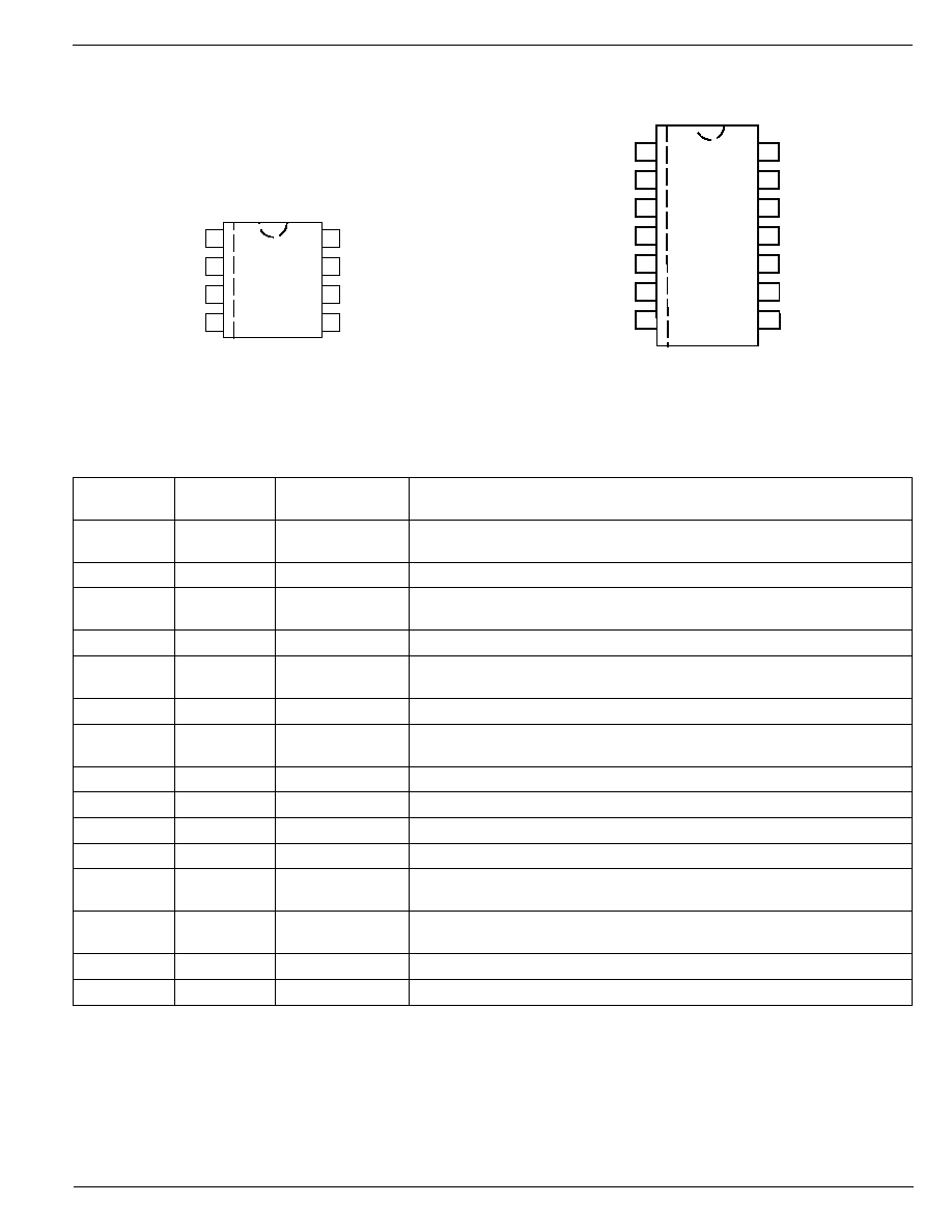
Pin Description
Pin Number
Pin Number
Pin Name
Pin Function
N, M, MM
-1BN, -1BM
1
1
COMP
Compensation: Connect external compensation network to modify the error
amplifier output.
2
NC
Not internally connected.
2
3
FB
Feedback (Input): Error amplifier input. Feedback is 2.5V at desired output
voltage.
4
NC
Not internally connected.
3
5
ISNS
Current Sense (Input): Current sense comparator input. Connect to current
sensing resistor or current transformer.
6
NC
Not internally connected.
4
7
RT/CT
Timing Resistor/Timing Capacitor: Connect external RC network to select
switching frequency.
5
GND
Ground: Combined analog and power ground.
8
PGND
Power Ground: N-channel driver transistor ground.
9
AGND
Analog Ground: Controller circuitry ground.
6
10
OUT
Power Output: Totem-pole output.
11
VD
Power Supply (Input): P-channel driver transistor supply input. Return to
power ground (PGND).
7
12
VDD
Analog Supply (Input): Controller circuitry supply input. Return to analog
ground (AGND).
13
NC
Not internally connected.
8
14
VREF
5V Reference (Output): Connect external RC network.
1
2
3
4
8
7
6
5
COMP
FB
ISNS
RT/CT
VREF
VDD
OUT
GND
MIC38C4x
2
NC
NC
13
3
FB
VDD
12
4
NC
VD
11
5
ISNS
OUT
10
6
NC
AGND
9
7
RT/CT
PGND
8
1
COMP
VREF
14
MIC38C4x-1
8-Pin DIP (N)
8-Lead SOIC (M)
8-Lead MM8TM (MM)
14-Pin DIP (-1BN)
14-Lead SOIC (-1BM)
Pin Configuration
MIC38C42/3/4/5
Micrel
MIC38C42/3/4/5
4
August 2000
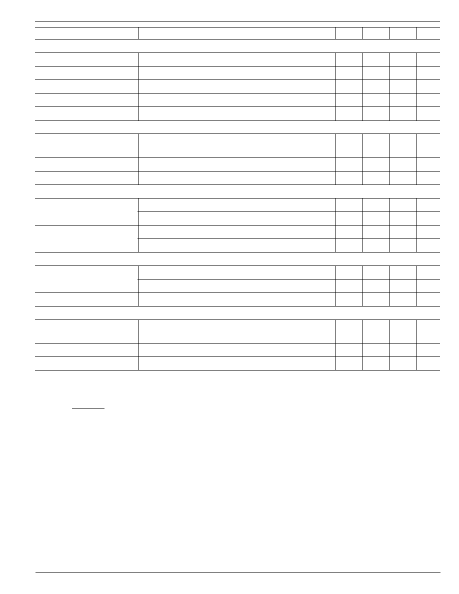
Electrical Characteristics
V
DD
= 15V, Note 4; R
T
= 11.0k; C
T
= 3.3nF; ≠40
∞C T
A
85∞C; unless noted
Parameter
Test Conditions
Min
Typ
Max
Units
Reference Section
Output Voltage
T
A
= 25
∞C, I
O
= 1mA
4.90
5.00
5.10
V
Line Regulation
12V
V
DD
18V, I
O
= 5
µA, Note 6
2
20
mV
Load Regulation
1
I
O
20mA
1
25
mV
Temp. Stability
Note 1
0.2
mV/
∞C
Total Output Variation
Line, Load, Temp., Note 1
4.82
5.18
V
Output Noise Voltage
10Hz
f 10kHz, T
A
= 25
∞C, Note 1
50
µV
Long Term Stability
T
A
= 125
∞C, 1000 hrs., Note 1
5
25
mV
Output Short Circuit
≠30
≠80
≠180
mA
Oscillator Section
Initial Accuracy
T
A
= 25
∞C, Note 5
49
52
55
kHz
Voltage Stability
12
V
DD
18V, Note 6
0.2
1.0
%
Temp. Stability
T
MIN
T
A
T
MAX
, Note 1
0.04
%/
∞C
Clock Ramp
T
A
= 25
∞C, V
RT/CT
= 2V
7.7
8.4
9.0
mA
Reset Current
T
A
= T
MIN
to T
MAX
7.2
8.4
9.5
mA
Amplitude
V
RT/CT
peak to peak
1.9
Vp-p
Error Amp Section
Input Voltage
V
COMP
= 2.5V
2.42
2.50
2.58
V
Input Bias Current
V
FB
= 5.0V
≠0.1
≠2
µA
A
VOL
2
V
O
4V
65
90
dB
Unity Gain Bandwidth
Note 1
0.7
1.0
MHz
PSRR
12
V
DD
18V
60
dB
Output Sink Current
V
FB
= 2.7V, V
COMP
= 1.1V
2
14
mA
Output Source Current
V
FB
= 2.3V, V
COMP
= 5V
≠0.5
≠1
mA
V
OUT
High
V
FB
= 2.3V, R
L
= 15k to ground
5
6.8
V
V
OUT
Low
V
FB
= 2.7V, R
L
= 15k to V
REF
0.1
1.1
V
Absolute Maximum Ratings
Zener Current (V
DD
) ................................................... 30mA
Operation at
18V may require
special precautions (Note 6).
Supply Voltage (V
DD
), Note 6 ....................................... 20V
Switch Supply Voltage (V
D
) .......................................... 20V
Current Sense Voltage (V
ISNS
) ..................... ≠0.3V to 5.5V
Feedback Voltage (V
FB
) ................................ ≠0.3V to 5.5V
Output Current, 38C42/3/4/5 (I
OUT
) ............................. 0.5A
Storage Temperature (T
A
) ....................... ≠65
∞C to +150∞C
Operating Ratings
Junction Temperature (T
J
) ........................................ 150
∞C
Package Thermal Resistance
8-Pin Plastic DIP
(
JA
) ....................................... 125
∞C/W
8-Pin MM8TM
(
JA
) ............................................. 250
∞C/W
8-Pin SOIC
(
JA
) ............................................... 170
∞C/W
14-Pin Plastic DIP
(
JA
) ....................................... 90
∞C/W
14-Pin SOIC
(
JA
) ............................................. 145
∞C/W
MIC38C42/3/4/5
Micrel
August 2000
5
MIC38C42/3/4/5
Parameter
Test Conditions
Min
Typ
Max
Units
Current Sense
Gain
Notes 2, 3
2.85
3.0
3.15
V/V
MaximumThreshold
V
COMP
= 5V, Note 2
0.9
1
1.1
V
PSRR
12
V
DD
18V, Note 2
70
dB
Input Bias Current
≠0.1
≠2
µA
Delay to Output
120
250
ns
Output
R
DS(ON)
High
I
SOURCE
= 200mA
20
R
DS(ON)
Low
I
SINK
= 200mA
11
Rise Time
T
A
= 25
∞C, C
L
= 1nF
40
80
ns
Fall Time
T
A
= 25
∞C, C
L
= 1nF
30
60
ns
Undervoltage Lockout
Start Threshold
MIC38C42/4
13.5
14.5
15.5
V
MIC38C43/5
7.8
8.4
9.0
V
Minimum Operating Voltage
MIC38C42/4
8
9
10
V
MIC38C43/5
7.0
7.6
8.2
V
Pulse Width Modulator
Maximum Duty Cycle
MIC38C42/3
94
96
%
MIC38C44/5
46
50
%
Minimum Duty Cycle
0
%
Total Standby Current
Start-Up Current
V
DD
= 13V for MIC38C42/44
50
200
µA
V
DD
= 7.5V for MIC38C43/45
Operating Supply Current
V
FB
= V
ISNS
= 0V
4.0
6.0
mA
Zener Voltage (V
DD
)
I
DD
= 25mA, Note 6
30
37
V
Note 1: These parameters, although guaranteed, are not 100% tested in production.
Note 2: Parameter measured at trip point of latch with V
EA
= 0.
Note 3: Gain defined as:
A =
V
V
(I
)
0
V
(I
)
0.8V
PIN1
TH
SNS
TH
SNS
;
Note 4: Adjust V
DD
above the start threshold before setting at 15V.
Note 5: Output frequency equals oscillator frequency for the MIC38C42 and MIC38C43. Output frequency for the MIC38C44, and
MIC38C45 equals one half the oscillator frequency.
Note 6: On 8-pin version, 20V is maximum input on pin 7, as this is also the supply pin for the output stage. On 14-pin version, 40V is
maximum for pin 12 and 20V maximum for pin 11.