
June 2000
1
MIC39100/39101/39102
MIC39100/39101/39102
Micrel
Ordering Information
Part Number
Voltage
Junction Temp. Range
Package
MIC39100-1.8BS
1.8V
≠40
∞
C to +125
∞
C
SOT-223
MIC39100-2.5BS
2.5V
≠40
∞
C to +125
∞
C
SOT-223
MIC39100-3.3BS
3.3V
≠40
∞
C to +125
∞
C
SOT-223
MIC39100-5.0BS
5.0V
≠40
∞
C to +125
∞
C
SOT-223
MIC39101-1.8BM
1.8V
≠40
∞
C to +125
∞
C
SOP-8
MIC39101-2.5BM
2.5V
≠40
∞
C to +125
∞
C
SOP-8
MIC39101-3.3BM
3.3V
≠40
∞
C to +125
∞
C
SOP-8
MIC39101-5.0BM
5.0V
≠40
∞
C to +125
∞
C
SOP-8
MIC39102BM
Adj.
≠40
∞
C to +125
∞
C
SOP-8
MIC39100/39101/39102
1A Low-Voltage Low-Dropout Regulator
Final Information
General Description
The MIC39100, MIC39101, and MIC39102 are 1A low-
dropout linear voltage regulators that provide low-voltage,
high-current output from an extremely small package. Utiliz-
ing Micrel's proprietary Super
eta PNPTM pass element, the
MIC39100/1/2 offers extremely low dropout (typically 410mV
at 1A) and low ground current (typically 11mA at 1A).
The MIC39100 is a fixed output regulator offered in the
SOT-223 package. The MIC39101 and MIC39102 are fixed
and adjustable regulators, respectively, in a thermally en-
hanced power 8-lead SOP (small outline package).
The MIC39100/1/2 is ideal for PC add-in cards that need to
convert from standard 5V to 3.3V, 3.3V to 2.5V or 2.5V to
1.8V. A guaranteed maximum dropout voltage of 630mV over
all operating conditions allows the MIC39100/1/2 to provide
2.5V from a supply as low as 3.13V and 1.8V from a supply
as low as 2.43V.
The MIC39100/1/2 is fully protected with overcurrent limiting,
thermal shutdown, and reversed-battery protection. Fixed
voltages of 5.0V, 3.3V, 2.5V, and 1.8V are available on
MIC39100/1 with adjustable output voltages to 1.24V on
MIC39102.
For other voltages, contact Micrel.
Typical Applications
Features
∑ Fixed and adjustable output voltages to 1.24V
∑ 410mV typical dropout at 1A
Ideal for 3.0V to 2.5V conversion
Ideal for 2.5V to 1.8V conversion
∑ 1A minimum guaranteed output current
∑ 1% initial accuracy
∑ Low ground current
∑ Current limiting and thermal shutdown
∑ Reversed-battery protection
∑ Reversed-leakage protection
∑ Fast transient response
∑ Low-profile SOT-223 package
∑ Power SO-8 package
Applications
∑ LDO linear regulator for PC add-in cards
∑ PowerPCTM power supplies
∑ High-efficiency linear power supplies
∑ SMPS post regulator
∑ Multimedia and PC processor supplies
∑ Battery chargers
∑ Low-voltage microcontrollers and digital logic
Super
eta PNP is a trademark of Micrel, Inc.
Micrel, Inc. ∑ 1849 Fortune Drive ∑ San Jose, CA 95131 ∑ USA ∑ tel + 1 (408) 944-0800 ∑ fax + 1 (408) 944-0970 ∑ http://www.micrel.com
IN
2.5V
V
IN
3.3V
10
µ
F
tantalum
OUT
GND
MIC39100
2.5V/1A Regulator
IN
R1
100k
2.5V
Error
Flag
Output
V
IN
3.3V
10
µ
F
tantalum
EN
OUT
FLG
GND
MIC39101
ENABLE
SHUTDOWN
2.5V/1A Regulator with Error Flag
IN
R1
1.5V
V
IN
2.5V
10
µ
F
tantalum
R2
EN
OUT
ADJ
GND
MIC39102
ENABLE
SHUTDOWN
1.5V/1A Adjustable Regulator
MIC39100/39101/39102
Micrel
MIC39100/39101/39102
2
June 2000
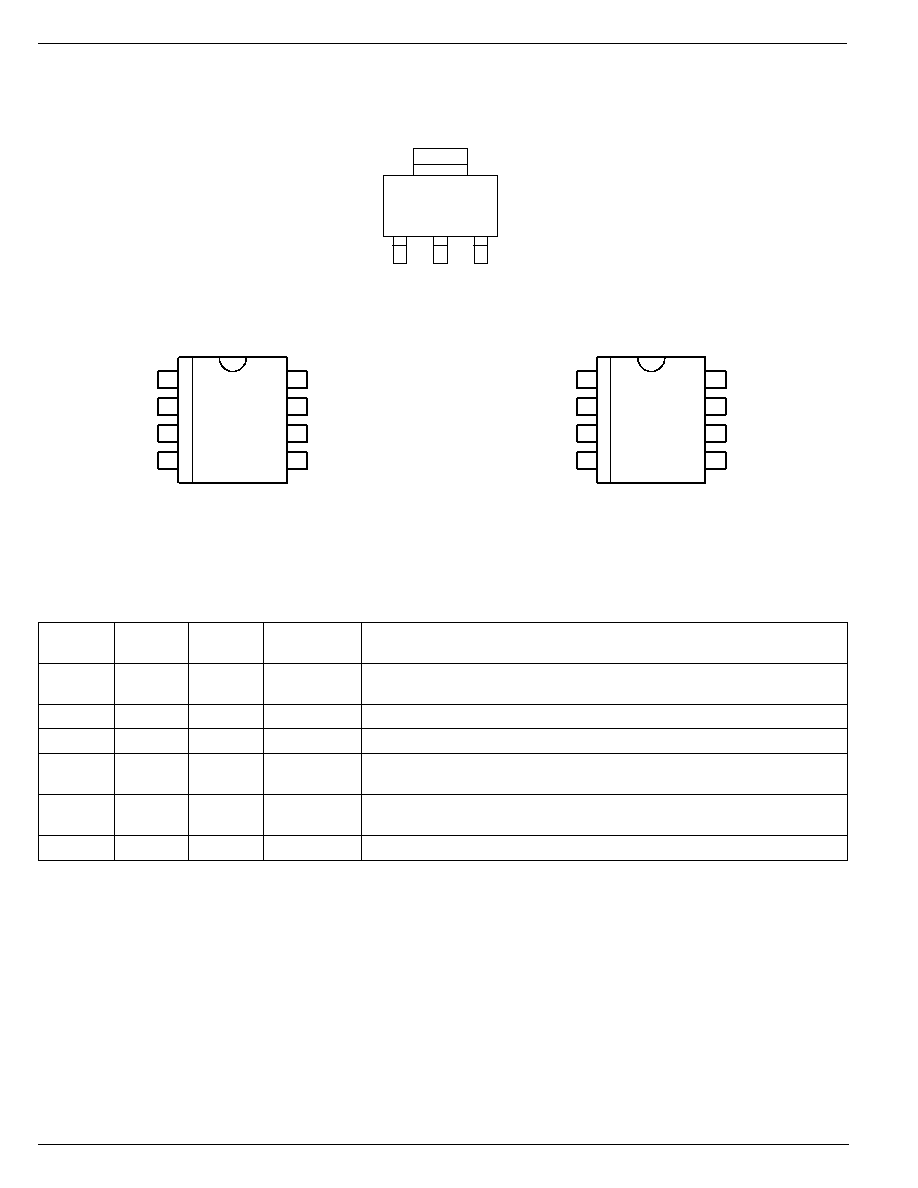
Pin Configuration
IN
OUT
GND
1
3
2
TAB
GND
MIC39100-x.x
Fixed
SOT-223 (S)
1
EN
IN
OUT
FLG
8
GND
GND
GND
GND
7
6
5
2
3
4
MIC39101-x.x
Fixed
SOP-8 (M)
1
EN
IN
OUT
ADJ
8
GND
GND
GND
GND
7
6
5
2
3
4
MIC39102
Adjustable
SOP-8 (M)
Pin Description
Pin No.
Pin No.
Pin No.
Pin Name
Pin Function
MIC39100
MIC39101
MIC39102
1
1
1
EN
Enable (Input): CMOS-compatible control input. Logic high = enable, logic
low or open = shutdown.
2
2
IN
Supply (Input)
3
3
3
OUT
Regulator Output
4
FLG
Flag (Output): Open-collector error flag output. Active low = output under-
voltage.
4
ADJ
Adjustment Input: Feedback input. Connect to resitive voltage-divider
network.
2,
TAB
5≠8
5≠8
GND
Ground
June 2000
3
MIC39100/39101/39102
MIC39100/39101/39102
Micrel
Electrical Characteristics
(Note 12)
V
IN
= V
OUT
+ 1V; V
EN
= 2.25V; T
J
= 25
∞
C, bold values indicate ≠40
∞
C
T
J
+125
∞
C; unless noted
Symbol
Parameter
Condition
Min
Typ
Max
Units
V
OUT
Output Voltage
10mA
≠1
1
%
10mA
I
OUT
1A, V
OUT
+ 1V
V
IN
8V
≠2
2
%
Line Regulation
I
OUT
= 10mA, V
OUT
+ 1V
V
IN
16V
0.06
0.5
%
Load Regulation
V
IN
= V
OUT
+ 1V, 10mA
I
OUT
1A,
0.2
1
%
V
OUT
/
T
Output Voltage Temp. Coefficient,
40
100
ppm/
∞
C
Note 5
V
DO
Dropout Voltage, Note 6
I
OUT
= 100mA,
V
OUT
= ≠1%
140
200
mV
250
mV
I
OUT
= 500mA,
V
OUT
= ≠1%
275
mV
I
OUT
= 750mA,
V
OUT
= ≠1%
330
500
mV
I
OUT
= 1A,
V
OUT
= ≠1%
550
mV
410
630
mV
I
GND
Ground Current, Note 7
I
OUT
= 100mA, V
IN
= V
OUT
+ 1V
400
µ
A
I
OUT
= 500mA, V
IN
= V
OUT
+ 1V
4
mA
I
OUT
= 750mA, V
IN
= V
OUT
+ 1V
6.5
mA
I
OUT
= 1A, V
IN
= V
OUT
+ 1V
11
20
mA
I
OUT(lim)
Current Limit
V
OUT
= 0V, V
IN
= V
OUT
+ 1V
1.8
2.5
A
Enable Input
V
EN
Enable Input Voltage
logic low (off)
0.8
V
logic high (on)
2.25
V
I
EN
Enable Input Current
V
EN
= 2.25V
1
15
30
µ
A
75
µ
A
V
EN
= 0.8V
2
µ
A
4
µ
A
Flag Output
I
FLG(leak)
Output Leakage Current
V
OH
= 16V
0.01
1
µ
A
2
µ
A
V
FLG(do)
Output Low Voltage
V
IN
= 2.250V, I
OL
, = 250
µ
A, Note 9
210
300
mV
400
mV
V
FLG
Low Threshold
% of V
OUT
93
%
High Threshold
% of V
OUT
99.2
%
Hysteresis
1
%
Absolute Maximum Ratings
(Note 1)
Supply Voltage (V
IN
) ..................................... ≠20V to +20V
Enable Voltage (V
EN
) .................................................. +20V
Storage Temperature (T
S
) ....................... ≠65
∞
C to +150
∞
C
Lead Temperature (soldering, 5 sec.) ....................... 260
∞
C
ESD, Note 3
Operating Ratings
(Note 2)
Supply Voltage (V
IN
) .................................. +2.25V to +16V
Enable Voltage (V
EN
) .................................................. +16V
Maximum Power Dissipation (P
D(max)
) ..................... Note 4
Junction Temperature (T
J
) ....................... ≠40
∞
C to +125
∞
C
Package Thermal Resistance
SOT-223
(
JC
) ..................................................... 15
∞
C/W
SOP-8
(
JC
) ......................................................... 20
∞
C/W

MIC39100/39101/39102
Micrel
MIC39100/39101/39102
4
June 2000
Symbol
Parameter
Condition
Min
Typ
Max
Units
MIC39102 Only
Reference Voltage
1.228
1.240
1.252
V
1.215
1.265
V
Note 10
1.203
1.277
V
Adjust Pin Bias Current
40
80
nA
120
nA
Reference Voltage
Note 7
20
ppm/
∞
C
Temp. Coefficient
Adjust Pin Bias Current
0.1
nA/
∞
C
Temp. Coefficient
Note 1.
Exceeding the absolute maximum ratings may damage the device.
Note 2.
The device is not guaranteed to function outside its operating rating.
Note 3.
Devices are ESD sensitive. Handling precautions recommended.
Note 4.
P
D(max)
= (T
J(max)
≠ T
A
)
˜
JA
, where
JA
depends upon the printed circuit layout. See "Applications Information."
Note 5.
Output voltage temperature coefficient is
V
OUT(worst case)
˜
(T
J(max)
≠ T
J(min)
) where T
J(max)
is +125
∞
C and T
J(min)
is ≠40
∞
C.
Note 6.
V
DO
= V
IN
≠ V
OUT
when V
OUT
decreases to 98% of its nominal output voltage with V
IN
= V
OUT
+ 1V. For output voltages below 2.25V, dropout
voltage is the input-to-output voltage differential with the minimum input voltage being 2.25V. Minimum input operating voltage is 2.25V.
Note 7.
I
GND
is the quiescent current. I
IN
= I
GND
+ I
OUT
.
Note 8.
V
EN
0.8V, V
IN
8V, and V
OUT
= 0V.
Note 9.
For a 2.5V device, V
IN
= 2.250V (device is in dropout).
Note 10. V
REF
V
OUT
(V
IN
≠ 1V), 2.25V
V
IN
16V, 10mA
I
L
1A, T
J
= T
MAX
.
Note 11. Thermal regulation is defined as the change in output voltage at a time t after a change in power dissipation is applied, excluding load or line
regulation effects. Specifications are for a 200mA load pulse at V
IN
= 16V for t = 10ms.
Note 12. Specification for packaged product only.
June 2000
5
MIC39100/39101/39102
MIC39100/39101/39102
Micrel
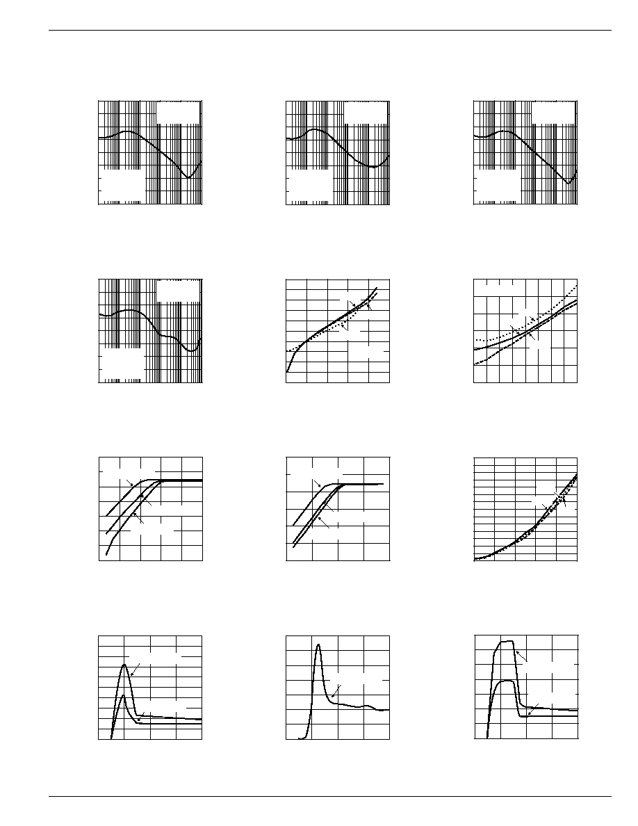
Typical Characteristics
0
20
40
60
80
1E+1 1E+2 1E+3 1E+4 1E+5 1E+6
PSRR (dB)
FREQUENCY (Hz)
Power Supply
Rejection Ratio
I
OUT
= 1A
C
OUT
= 10
µ
F
C
IN
= 0
V
IN
= 5V
V
OUT
= 3.3V
10
100
1k
10k
100k
1M
0
20
40
60
80
1E+1 1E+2 1E+3 1E+4 1E+5 1E+6
PSRR (dB)
FREQUENCY (Hz)
Power Supply
Rejection Ratio
I
OUT
= 1A
C
OUT
= 47
µ
F
C
IN
= 0
V
IN
= 5V
V
OUT
= 3.3V
10
100
1k
10k
100k
1M
0
20
40
60
80
1E+1 1E+2 1E+3 1E+4 1E+5 1E+6
PSRR (dB)
FREQUENCY (Hz)
Power Supply
Rejection Ratio
I
OUT
= 1A
C
OUT
= 10
µ
F
C
IN
= 0
V
IN
= 3.3V
V
OUT
= 2.5V
10
100
1k
10k
100k
1M
0
20
40
60
80
1E+1 1E+2 1E+3 1E+4 1E+5 1E+6
PSRR (dB)
FREQUENCY (Hz)
Power Supply
Rejection Ratio
I
OUT
= 1A
C
OUT
= 47
µ
F
C
IN
= 0
V
IN
= 3.3V
V
OUT
= 2.5V
10
100
1k
10k
100k
1M
0
50
100
150
200
250
300
350
400
450
500
0
250
500
750
1000 1250
DROPOUT VOLTAGE (mV)
OUTPUT CURRENT (mA)
Dropout Voltage
vs. Output Current
2.5V
3.3V
T
A
= 25
∞
C
1.8V
300
350
400
450
500
550
600
-40 -20 0
20 40 60 80 100 120
DROPOUT VOLTAGE (mV)
TEMPERATURE (
∞
C)
Dropout Voltage
vs. Temperature
3.3V
2.5V
I
LOAD
= 1A
1.8V
1.4
1.6
1.8
2.0
2.2
2.4
2.6
2.8
2
2.3
2.6
2.9
3.2
3.5
OUTPUT VOLTAGE (V)
SUPPLY VOLTAGE (V)
Dropout Characteristics
(2.5V)
ILOAD
=100mA
ILOAD
=750mA
ILOAD
=1A
2.4
2.6
2.8
3.0
3.2
3.4
3.6
2.8
3.2
3.6
4.0
4.4
OUTPUT VOLTAGE (V)
SUPPLY VOLTAGE (V)
Dropout Characteristics
(3.3V)
ILOAD
=100mA
ILOAD
=750mA
ILOAD
=1A
0
2
4
6
8
10
12
14
0
200
400
600
800
1000
GROUND CURRENT (mA)
OUTPUT CURRENT (mA)
Ground Current
vs. Output Current
2.5V
3.3V
1.8V
0
0.2
0.4
0.6
0.8
1.0
1.2
1.4
1.6
1.8
2.0
0
2
4
6
8
GROUND CURRENT (mA)
SUPPLY VOLTAGE (V)
Ground Current
vs. Supply Voltage (2.5V)
ILOAD
=
100mA
ILOAD
=
10mA
0
0.2
0.4
0.6
0.8
1.0
1.2
1.4
0
2
4
6
8
GROUND CURRENT (mA)
SUPPLY VOLTAGE (V)
Ground Current
vs. Supply Voltage (3.3V)
ILOAD
=100mA
ILOAD
=10mA
0
5
10
15
20
25
30
35
0
2
4
6
8
GROUND CURRENT (mA)
SUPPLY VOLTAGE (V)
Ground Current
vs. Supply Voltage (2.5V)
ILOAD
=1A
MIC39100/39101/39102
Micrel
MIC39100/39101/39102
6
June 2000
0
10
20
30
40
50
0
2
4
6
8
GROUND CURRENT (mA)
SUPPLY VOLTAGE (V)
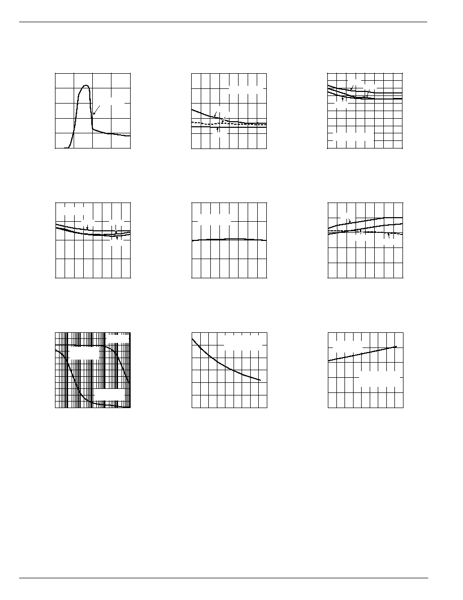
Ground Current
vs. Supply Voltage (3.3V)
ILOAD
=1A
0
0.2
0.4
0.6
0.8
1.0
-40 -20 0
20 40 60 80 100 120
GROUND CURRENT (mA)
TEMPERATURE (
∞
C)
Ground Current
vs. Temperature
3.3V
ILOAD
=
10mA
2.5V
1.8V
0
5
10
15
20
-40 -20 0
20 40 60 80 100 120
GROUND CURRENT (mA)
TEMPERATURE (
∞
C)
Ground Current
vs. Temperature
3.3V
2.5V
I
LOAD
= 1A
1.8V
3.20
3.25
3.30
3.35
3.40
-40 -20 0
20 40 60 80 100 120
OUTPUT VOLTAGE (V)
TEMPERATURE (
∞
C)
Output Voltage
vs. Temperature
Typical 3.3V
Device
0
0.5
1.0
1.5
2.0
2.5
-40 -20 0
20 40 60 80 100 120
SHORT CIRCUIT CURRENT (A)
TEMPERATURE (
∞
C)
Short Circuit
vs. Temperature
3.3V
2.5V
1.8V
0
0.5
1.0
1.5
2.0
2.5
3.0
3.5
4.0
4.5
5.0
-40 -20 0
20 40 60 80 100 120
GROUND CURRENT (mA)
TEMPERATURE (
∞
C)
Ground Current
vs. Temperature
3.3V
2.5V
I
LOAD
= 500mA
1.8V
0
1
2
3
4
5
6
0.01 0.1
1
10
100 100010000
FLAG VOLTAGE (V)
RESISTANCE (k
)
Error Flag
Pull-Up Resistor
V
IN
= 5V
FLAG HIGH
(OK)
FLAG LOW
(FAULT)
0
2
4
6
8
10
12
-40 -20 0 20 40 60 80 100120140
ENABLE CURRENT
µ
A)
TEMPERATURE (
∞
C)
Enable Current
vs. Temperature
V
IN
= V
OUT
+ 1V
V
EN
= 2.4V
0
50
100
150
200
250
-40 -20 0 20 40 60 80 100120140
FLAG VOLTAGE (mV)
TEMPERATURE (
∞
C)
Flag-Low Voltage
vs. Temperature
V
IN
= 2.25V
R
PULL-UP
= 22k
FLAG-LOW
VOLTAGE

June 2000
7
MIC39100/39101/39102
MIC39100/39101/39102
Micrel
Functional Characteristics
Load Transient Response
TIME (250
µ
s/div.)
LO
AD CURRENT
(500mA/div
.
)
OUTPUT V
O
L
T
A
G
E
(200mV/div
.
)
V
OUT
= 2.5V
C
OUT
= 10
µ
F
1A
100mA
Load Transient Response
TIME (500
µ
s/div.)
LO
AD CURRENT
(500mA/div
.
)
OUTPUT V
O
L
T
A
G
E
(200mV/div
.
)
V
OUT
= 2.5V
C
OUT
= 47
µ
F
1A
10mA
Line Transient Response
TIME (25
µ
s/div.)
INPUT V
O
L
T
A
G
E
(2V/div
.
)
OUTPUT V
O
L
T
A
G
E
(50mV/div
.
)
V
OUT
= 2.5V
C
OUT
= 10
µ
F

MIC39100/39101/39102
Micrel
MIC39100/39101/39102
8
June 2000
Functional Diagrams
Ref.
18V
OV I
LIMIT
Thermal
Shut-
down
1.240V
IN
OUT
GND
MIC39100
MIC39100 Fixed Regulator Block Diagram
Ref.
18V
O.V.
I
LIMIT
Thermal
Shut-
down
1.240V
1.180V
EN
IN
FLAG
GND
OUT
MIC39101
MIC39101 Fixed Regulator with Flag and Enable Block Diagram
Ref.
18V
O.V.
I
LIMIT
Thermal
Shut-
down
1.240V
EN
IN
GND
OUT
ADJ
MIC39102
MIC39102 Adjustable Regulator Block Diagram
June 2000
9
MIC39100/39101/39102
MIC39100/39101/39102
Micrel
Applications Information
The MIC39100/1/2 is a high-performance low-dropout volt-
age regulator suitable for moderate to high-current voltage
regulator applications. Its 630mV dropout voltage at full load
and overtemperature makes it especially valuable in battery-
powered systems and as high-efficiency noise filters in post-
regulator applications. Unlike older NPN-pass transistor de-
signs, where the minimum dropout voltage is limited by the
base-to-emitter voltage drop and collector-to-emitter satura-
tion voltage, dropout performance of the PNP output of these
devices is limited only by the low V
CE
saturation voltage.
A trade-off for the low dropout voltage is a varying base drive
requirement. Micrel's Super
eta PNPTM process reduces
this drive requirement to only 2% of the load current.
The MIC39100/1/2 regulator is fully protected from damage
due to fault conditions. Linear current limiting is provided.
Output current during overload conditions is constant. Ther-
mal shutdown disables the device when the die temperature
exceeds the maximum safe operating temperature. Tran-
sient protection allows device (and load) survival even when
the input voltage spikes above and below nominal. The
output structure of these regulators allows voltages in excess
of the desired output voltage to be applied without reverse
current flow.
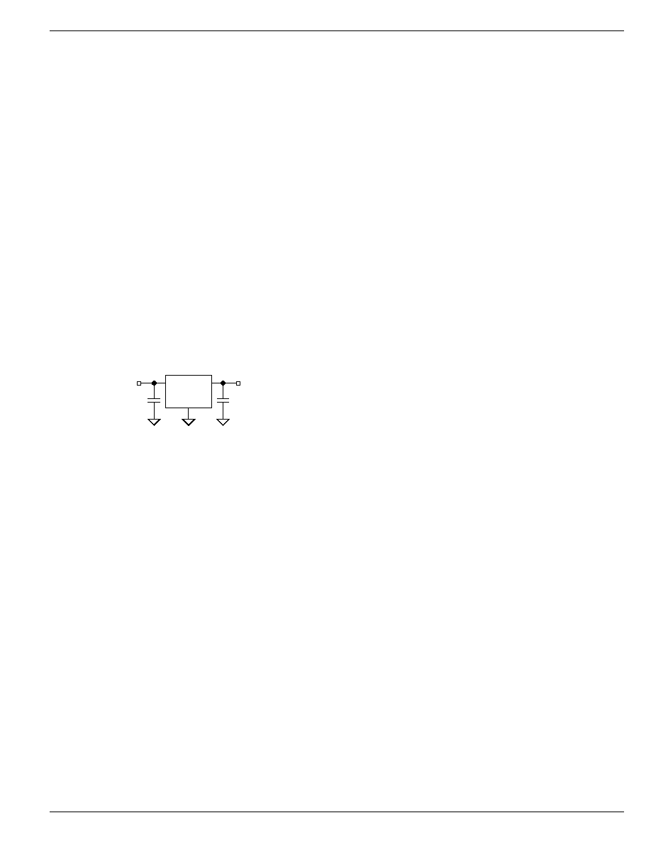
MIC39100-x.x
IN
OUT
GND
C
IN
C
OUT
V
IN
V
OUT
Figure 1. Capacitor Requirements
Output Capacitor
The MIC39100/1/2 requires an output capacitor to maintain
stability and improve transient response. Proper capacitor
selection is important to ensure proper operation. The
MIC39100/1/2 output capacitor selection is dependent upon
the ESR (equivalent series resistance) of the output capacitor
to maintain stability. When the output capacitor is 10
µ
F or
greater, the output capacitor should have an ESR less than
2
. This will improve transient response as well as promote
stability. Ultra-low-ESR capacitors (<100m
), such as ce-
ramic chip capacitors, may promote instability. These very
low ESR levels may cause an oscillation and/or underdamp-
ed transient response. A low-ESR solid tantalum capacitor
works extremely well and provides good transient response
and stability over temperature. Aluminum electrolytics can
also be used, as long as the ESR of the capacitor is <2
.
The value of the output capacitor can be increased without
limit. Higher capacitance values help to improve transient
response and ripple rejection and reduce output noise.
Input Capacitor
An input capacitor of 1
µ
F or greater is recommended when
the device is more than 4 inches away from the bulk ac supply
capacitance or when the supply is a battery. Small, surface
mount, ceramic chip capacitors can be used for bypassing.
Larger values will help to improve ripple rejection by bypass-
ing the input to the regulator, further improving the integrity of
the output voltage.
Error Flag
The MIC39101 features an error flag (FLG), which monitors
the output voltage and signals an error condition when this
voltage drops 5% below its expected value. The error flag is
an open-collector output that pulls low under fault conditions
and may sink up to 10mA. Low output voltage signifies a
number of possible problems, including an overcurrent fault
(the device is in current limit) or low input voltage. The flag
output is inoperative during overtemperature conditions. A
pull-up resistor from FLG to either V
IN
or V
OUT
is required for
proper operation. For information regarding the minimum and
maximum values of pull-up resistance, refer to the graph in
the typical characteristics section of the data sheet.
Enable Input
The MIC39101 and MIC39102 versions feature an active-
high enable input (EN) that allows on-off control of the
regulator. Current drain reduces to "zero" when the device is
shutdown, with only microamperes of leakage current. The
EN input has TTL/CMOS compatible thresholds for simple
logic interfacing. EN may be directly tied to V
IN
and pulled up
to the maximum supply voltage
Transient Response and 3.3V to 2.5V or 2.5V to 1.8V
Conversion
The MIC39100/1/2 has excellent transient response to varia-
tions in input voltage and load current. The device has been
designed to respond quickly to load current variations and
input voltage variations. Large output capacitors are not
required to obtain this performance. A standard 10
µ
F output
capacitor, preferably tantalum, is all that is required. Larger
values help to improve performance even further.
By virtue of its low-dropout voltage, this device does not
saturate into dropout as readily as similar NPN-based de-
signs. When converting from 3.3V to 2.5V or 2.5V to 1.8V, the
NPN based regulators are already operating in dropout, with
typical dropout requirements of 1.2V or greater. To convert
down to 2.5V or 1.8V without operating in dropout, NPN-
based regulators require an input voltage of 3.7V at the very
least. The MIC39100 regulator will provide excellent perfor-
mance with an input as low as 3.0V or 2.5V respectively. This
gives the PNP based regulators a distinct advantage over
older, NPN based linear regulators.
Minimum Load Current
The MIC39100/1/2 regulator is specified between finite loads.
If the output current is too small, leakage currents dominate
and the output voltage rises. A 10mA minimum load current
is necessary for proper regulation.

MIC39100/39101/39102
Micrel
MIC39100/39101/39102
10
June 2000
Adjustable Regulator Design
IN
R1
V
OUT
V
IN
C
OUT
R2
EN
OUT
ADJ
GND
MIC39102
ENABLE
SHUTDOWN
V
1.240V 1
R1
R2
OUT
=
+
Figure 2. Adjustable Regulator with Resistors
The MIC39102 allows programming the output voltage any-
where between 1.24V and the 16V maximum operating rating
of the family. Two resistors are used. Resistors can be quite
large, up to 1M
, because of the very high input impedance
and low bias current of the sense comparator: The resistor
values are calculated by:
R1 R2
V
1.240
1
OUT
=
-
Where V
O
is the desired output voltage. Figure 2 shows
component definition. Applications with widely varying load
currents may scale the resistors to draw the minimum load
current required for proper operation (see above).
Power SOP-8 Thermal Characteristics
One of the secrets of the MIC39101/2's performance is its
power SO-8 package featuring half the thermal resistance of
a standard SO-8 package. Lower thermal resistance means
more output current or higher input voltage for a given
package size.
Lower thermal resistance is achieved by joining the four
ground leads with the die attach paddle to create a single-
piece electrical and thermal conductor. This concept has
been used by MOSFET manufacturers for years, proving
very reliable and cost effective for the user.
Thermal resistance consists of two main elements,
JC
(junction-to-case thermal resistance) and
CA
(case-to-ambi-
ent thermal resistance). See Figure 3.
JC
is the resistance
from the die to the leads of the package.
CA
is the resistance
from the leads to the ambient air and it includes
CS
(case-to-
sink thermal resistance) and
SA
(sink-to-ambient thermal
resistance).
Using the power SOP-8 reduces the
JC
dramatically and
allows the user to reduce
CA
. The total thermal resistance,
JA
(junction-to-ambient thermal resistance) is the limiting
factor in calculating the maximum power dissipation capabil-
ity of the device. Typically, the power SOP-8 has a
JC
of
20
∞
C/W, this is significantly lower than the standard SOP-8
which is typically 75
∞
C/W.
CA
is reduced because pins 5
through 8 can now be soldered directly to a ground plane
which significantly reduces the case-to-sink thermal resis-
tance and sink to ambient thermal resistance.
Low-dropout linear regulators from Micrel are rated to a
maximum junction temperature of 125
∞
C. It is important not
to exceed this maximum junction temperature during opera-
tion of the device. To prevent this maximum junction tempera-
ture from being exceeded, the appropriate ground plane heat
sink must be used.
JA
JC
CA
printed circuit board
ground plane
heat sink area
SOP-8
AMBIENT
Figure 3. Thermal Resistance
Figure 4 shows copper area versus power dissipation with
each trace corresponding to a different temperature rise
above ambient.
From these curves, the minimum area of copper necessary
for the part to operate safely can be determined. The maxi-
mum allowable temperature rise must be calculated to deter-
mine operation along which curve.
0
100
200
300
400
500
600
700
800
900
0
0.25 0.50 0.75 1.00 1.25 1.50
COPPER AREA (mm
2
)
POWER DISSIPATION (W)
40
∞
C
50
∞
C
55
∞
C
65
∞
C
75
∞
C
85
∞
C
100
∞
C
T
JA
=
Figure 4. Copper Area vs. Power-SOP
Power Dissipation
0
100
200
300
400
500
600
700
800
900
0
0.25 0.50 0.75 1.00 1.25 1.50
COPPER AREA (mm
2
)
POWER DISSIPATION (W)
T
A
= 85
∞
C
50
∞
C
25
∞
C
T
J
= 125
∞
C
Figure 5. Copper Area vs. Power-SOP
Power Dissipation

June 2000
11
MIC39100/39101/39102
MIC39100/39101/39102
Micrel
T = T
J(max)
≠ T
A(max)
T
J(max)
= 125
∞
C
T
A(max)
= maximum ambient operating temperature
For example, the maximum ambient temperature is 50
∞
C, the
T is determined as follows:
T = 125
∞
C ≠ 50
∞
C
T = 75
∞
C
Using Figure 4, the minimum amount of required copper can
be determined based on the required power dissipation.
Power dissipation in a linear regulator is calculated as fol-
lows:
P
D
= (V
IN
≠ V
OUT
) I
OUT
+ V
IN
∑ I
GND
If we use a 2.5V output device and a 3.3V input at an output
current of 1A, then our power dissipation is as follows:
P
D
= (3.3V ≠ 2.5V)
◊
1A + 3.3V
◊
11mA
P
D
= 800mW + 36mW
P
D
= 836mW
From Figure 4, the minimum amount of copper required to
operate this application at a
T of 75
∞
C is 160mm
2
.
Quick Method
Determine the power dissipation requirements for the design
along with the maximum ambient temperature at which the
device will be operated. Refer to Figure 5, which shows safe
operating curves for three different ambient temperatures:
25
∞
C, 50
∞
C and 85
∞
C. From these curves, the minimum
amount of copper can be determined by knowing the maxi-
mum power dissipation required. If the maximum ambient
temperature is 50
∞
C and the power dissipation is as above,
836mW, the curve in Figure 5 shows that the required area of
copper is 160mm
2
.
The
JA
of this package is ideally 63
∞
C/W, but it will vary
depending upon the availability of copper ground plane to
which it is attached.
MIC39100/39101/39102
Micrel
MIC39100/39101/39102
12
June 2000
MICREL INC.
1849 FORTUNE DRIVE
SAN JOSE, CA 95131
USA
TEL
+ 1 (408) 944-0800
FAX
+ 1 (408) 944-0970
WEB
http://www.micrel.com
This information is believed to be accurate and reliable, however no responsibility is assumed by Micrel for its use nor for any infringement of patents or
other rights of third parties resulting from its use. No license is granted by implication or otherwise under any patent or patent right of Micrel Inc.
© 2000 Micrel Incorporated
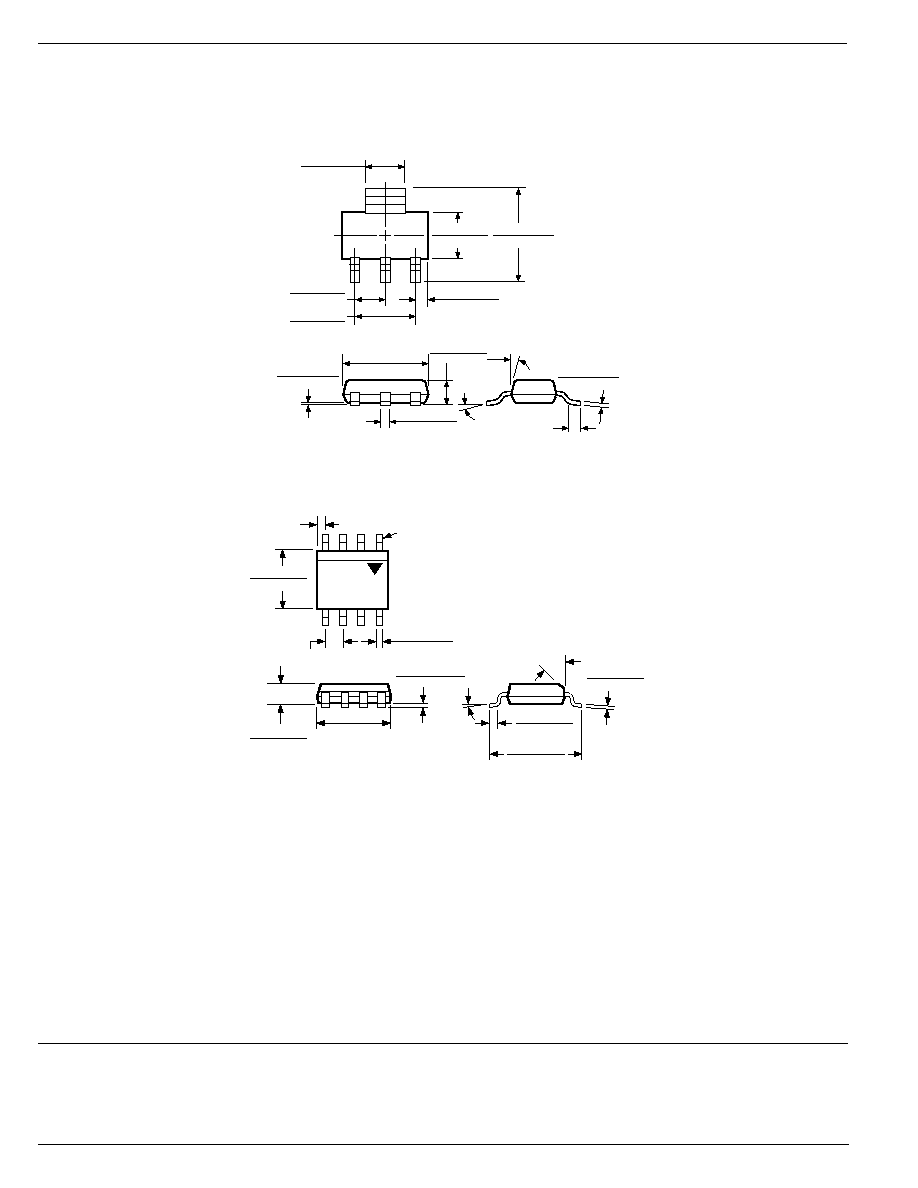
Package Information
16
∞
10
∞
0.84 (0.033)
0.64 (0.025)
1.04 (0.041)
0.85 (0.033)
2.41 (0.095)
2.21 (0.087)
4.7 (0.185)
4.5 (0.177)
6.70 (0.264)
6.30 (0.248)
7.49 (0.295)
6.71 (0.264)
3.71 (0.146)
3.30 (0.130)
3.15 (0.124)
2.90 (0.114)
10
∞
MAX
0.10 (0.004)
0.02 (0.0008)
0.38 (0.015)
0.25 (0.010)
C
L
DIMENSIONS:
MM (INCH)
C
L
1.70 (0.067)
1.52 (0.060)
0.91 (0.036) MIN
SOT-223 (S)
45
∞
0
∞
≠8
∞
0.244 (6.20)
0.228 (5.79)
0.197 (5.0)
0.189 (4.8)
SEATING
PLANE
0.026 (0.65)
MAX
)
0.010 (0.25)
0.007 (0.18)
0.064 (1.63)
0.045 (1.14)
0.0098 (0.249)
0.0040 (0.102)
0.020 (0.51)
0.013 (0.33)
0.157 (3.99)
0.150 (3.81)
0.050 (1.27)
TYP
PIN 1
DIMENSIONS:
INCHES (MM)
0.050 (1.27)
0.016 (0.40)
8-Lead SOP (M)