 | –≠–ª–µ–∫—Ç—Ä–æ–Ω–Ω—ã–π –∫–æ–º–ø–æ–Ω–µ–Ω—Ç: MIC4102 | –°–∫–∞—á–∞—Ç—å:  PDF PDF  ZIP ZIP |

MIC4102
100V Half Bridge MOSFET Driver
with Anti-Shoot Through Protection
PRELIMINARY SPECIFICATIONS
Power, Connect and Protect is a registered trademark of Micrel, Inc.
Micrel Inc. ∑ 2180 Fortune Drive ∑ San Jose, CA 95131 ∑ USA ∑ tel +1 (408) 944-0800 ∑ fax + 1 (408) 474-1000 ∑ http://www.micrel.com
October 2004
M9999-102004
General Description
The MIC4102 is a high frequency, 100V Half Bridge
MOSFET driver IC featuring internal anti-shoot-through
protection. The low-side and high-side gate drivers are
controlled by a single input signal to the PWM pin. The
MIC4102 implements adaptive anti-shoot-through circuitry
to optimize the switching transitions for maximum
efficiency. The single input control also reduces system
complexity and greatly simplifies the overall design.
The MIC4102 also features a low-side drive disable pin.
This gives the MIC4102 the capability to operate in a non-
synchronous buck mode. This feature allows the MIC4102
to start up into applications where a bias voltage may
already be present without pulling the output voltage down.
Under-voltage protection on both the low-side and high-
side supplies forces the outputs low. An on-chip boot-strap
diode eliminates the discrete diode required with other
driver ICs.
The MIC4102 is available in the SOIC-8L package with a
junction operating range from ≠40
∞
C to +125
∞
C.
Data sheets and support documentation can be found on
Micrel's web site at www.micrel.com.
Features
∑
Drives high- and low-side N-Channel MOSFETs with
single input
∑
Adaptive anti-shoot-through protection
∑
Low side drive disable pin
∑
Bootstrap supply voltage to 118V DC
∑
Supply voltage up to 16V
∑
TTL input thresholds
∑
On-chip bootstrap diode
∑
Fast 30ns propagation times
∑
Drives 1000pF load with 10ns rise and fall times
∑
Low
power
consumption
∑
Supply under-voltage protection
∑
2.5
pull up , 1.5
pull down output resistance
∑
Space saving SOIC-8L package
∑
≠40
∞
C to +125
∞
C junction temperature range
Applications
∑
High voltage buck converters
∑
2-stage push-pull power converters
∑
Networking / Telecom power supplies
∑
Automotive power supplies
___________________________________________________________________________________________________________
Typical Application
100V Buck Regulator Solution
Micrel, Inc.
MIC4102
October 2004
2
M9999-102004
Ordering Information
Part Number
Input
Junction Temp. Range
Package
MIC4102BM
TTL
≠40∞ to +125∞C
SOIC-8L
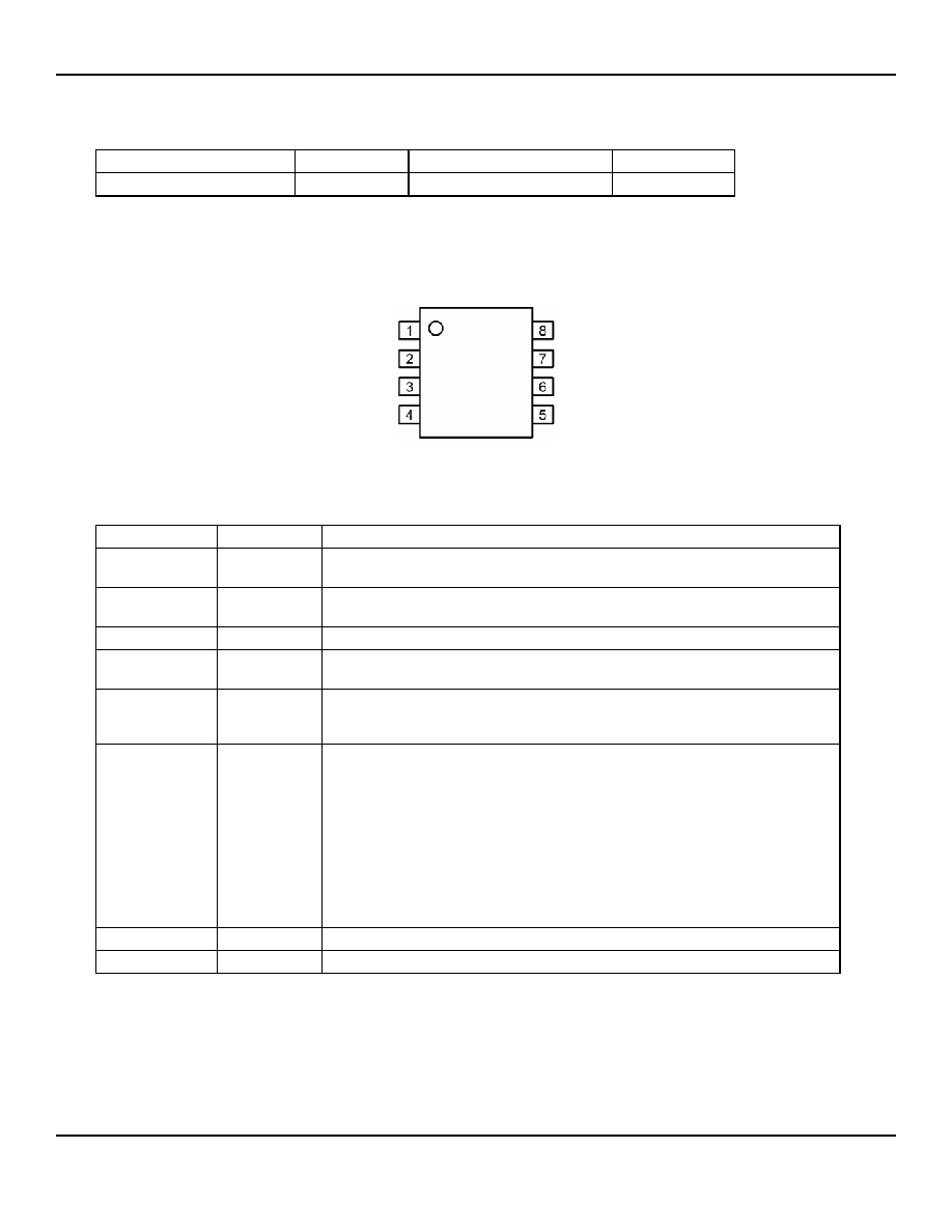
Pin Configuration
SOIC-8L (M))
Pin Description
Pin Number
Pin Name
Pin Function
1 VDD Positive Supply to lower gate drivers. Decouple this pin to VSS (Pin 7). Bootstrap
diode connected to HB (pin 2).
2 HB
High-Side Bootstrap supply. External bootstrap capacitor is required. Connect
positive side of bootstrap capacitor to this pin. Bootstrap diode is on-chip.
3
HO
High-Side Output. Connect to gate of High-Side power MOSFET.
4 HS
High-Side Source connection. Connect to source of High-Side power MOSFET.
Connect negative side of bootstrap capacitor to this pin.
5 PWM Control Input. PWM high signal makes high-side HO output high, and low-side
LO output low. PWM low signal makes high-side HO output low, and low-side
LO output high.
6 LS
Low-Side Disable. When pulled low, this control signal immediately terminates
the low-side LO output drive. The low-side LO output drive will remain low until
this signal is removed. HS drive is not affected by the LS signal. Here is the
logic table:
LS PWM LO HO
0 0 0 0
0 1 0 1
1 0 1 0
1 1 0 1
7
VSS
Chip negative supply, generally will be grounded.
8
LO
Low-Side Output. Connect to gate of Low-Side power MOSFET.
VDD
HB
HO
HS
LO
VSS
LS
PWM
Micrel, Inc.
MIC4102
October 2004
3
M9999-102004
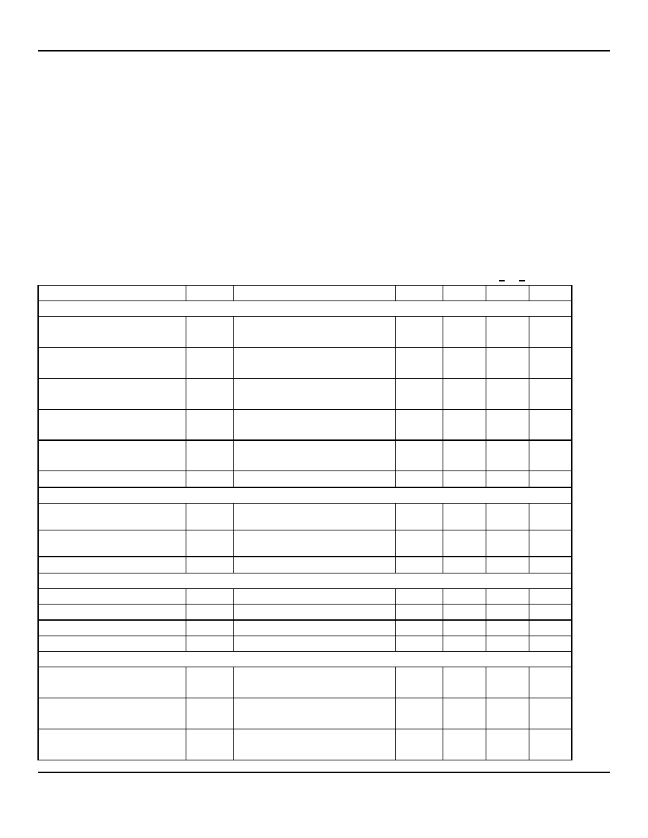
Absolute Maximum Ratings
(1)
Supply Voltage (V
DD
, V
HB
≠ V
HS
) ...................... -0.3V to 18V
Input Voltages (V
PWM,
V
LS
) ..................... -0.3V to V
DD
+ 0.3V
Voltage on LO (V
LO
) .............................. -0.3V to V
DD
+ 0.3V
Voltage on HO (V
HO
) ......................V
HS
- 0.3V to V
HB
+ 0.3V
Voltage on HS (continuous) .............................. -1V to 110V
Voltage on HB ..............................................................118V
Average Current in VDD to HB Diode.......................100mA
Junction Temperature (T
J
) ........................≠55∞C to +150∞C
Storage Temperature (T
s
) ..........................-60∞C to +150∞C
EDS Rating
(3)
..............................................................Note 3
Operating Ratings
(2)
Supply Voltage (V
DD
)........................................ +9V to +16V
Voltage on HS ................................................... -1V to 100V
Voltage on HS (repetitive transient) .................. -5V to 105V
HS Slew Rate............................................................ 50V/ns
Voltage on HB ...................................V
HS
+ 8V to V
HS
+ 16V
and............................................ V
DD
- 1V to V
DD
+ 100V
Junction Temperature (T
J
) ........................ ≠40∞C to +125∞C
Junction Thermal Resistance
SOIC-8L
(
JA
)...................................................140∞C/W
Electrical Characteristics
(4)
V
DD
= V
HB
= 12V; V
SS
= V
HS
= 0V; No load on LO or HO; T
A
= 25∞C; unless noted. Bold values indicate ≠40∞C< T
J
< +125∞C
.
Parameter Symbol
Condition
Min
Typ
Max
Units
Supply Current
V
DD
Quiescent Current
I
DD
PWM = 0V
150
450
600
µ
A
V
DD
Operating Current
I
DDO
f = 500kHz
3
3.5
4.0
mA
Total HB Quiescent Current
I
HB
PWM = 0V
25
150
200
µ
A
Total HB Operating Current
I
HBO
f = 500kHz
1.5
2.5
3
mA
HB to V
SS
Current, Quiescent
I
HBS
V
HS
= V
HB
= 110V
0.05 1
30
µ
A
HB to V
SS
Current, Operating
I
HBSO
f = 500kHz
10
µ
A
Input Pins (TTL)
Low Level Input Voltage
Threshold
V
IL
0.8
1.5
V
High Level Input Voltage
Threshold
V
IH
1.5
2.2
V
Input Pull-down Resistance
R
I
100
200
500
K
Under Voltage Protection
V
DD
Rising Threshold
V
DDR
6.5
7.3
8.0
V
V
DD
Threshold Hysteresis
V
DDH
0.5
V
HB Rising Threshold
V
HBR
6.0
7.0
8.0
V
HB Threshold Hysteresis
V
HBH
0.4
V
Boost Strap Diode
Low-Current Forward Voltage
V
DL
I
VDD-HB
= 100
µ
A
0.4
0.55
0.70
V
Low-Current Forward Voltage
V
DH
I
VDD-HB
= 100mA
0.7
0.8
1.0
V
Dynamic Resistance
R
D
I
VDD-HB
= 100mA
1.0
1.5
2.0
Micrel, Inc.
MIC4102
October 2004
4
M9999-102004
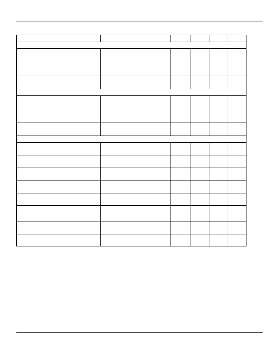
Parameter Symbol
Condition
Min Typ Max
LO Gate Driver
Low Level Output Voltage
V
OLL
I
LO
= 160mA
0.18
0.3
0.4
V
High Level Output Voltage
V
OHL
I
LO
= -100mA, V
OHL
= V
DD
- V
LO
0.25
0.3
0.45
V
Peak Sink Current
I
OHL
V
LO
= 0V
3
A
Peak Source Current
I
OLL
V
LO
= 12V
2
A
HO Gate Driver
Low Level Output Voltage
V
OLH
I
HO
= 160mA
0.22
0.3
0.4
V
High Level Output Voltage
V
OHH
I
HO
= -100mA, V
OHH
= V
HB
≠ V
HO
0.25
0.3
0.45
V
Peak Sink Current
I
OHH
V
HO
= 0V
3
A
Peak Source Current
I
OLH
V
HO
= 12V
2
A
Switching Specifications (Anti-Shoot-Through Circuitry)
Delay between PWM going high
to LO going low
t
LOOFF
30
45
60
ns
Voltage threshold for LO
MOSFET to be considered OFF
V
LOOFF
1.7
V
Delay between LO OFF to HO
going High
t
HOON
30
50
60
ns
Delay between PWM going Low
to HO going low
t
HOOFF
45
65
70
ns
Switch Node Voltage Threshold
when HO turns off
V
SWth
1
2.5
4
V
Delay between HO MOSFET
being considered off to LO
turning ON
t
LOON
30
60
70
ns
Delay between LS going low
and LO turning OFF
t
LSOFF
C
L
= 1000pF
36
45
70
ns
Forced LO ON, if V
LOTH
is not
detected
t
SWTO
120
250
450
ns

Micrel, Inc.
MIC4102
October 2004
5
M9999-102004
Parameter Symbol
Condition
Min
Typ
Max
Units
Switching Specifications
Either Output Rise Time (3V to
9V)
t
R
C
L
= 1000pF
10
ns
Either Output Fall Time (3V to
9V)
t
F
C
L
= 1000pF
6
ns
Either Output Rise Time (3V to
9V)
t
R
C
L
= 0.1
µ
F
0.33
0.6
0.8
µ
s
Either Output Fall Time (3V to
9V)
t
F
C
L
= 0.1
µ
F
0.2
0.3
0.4
µ
s
Minimum Input Pulse Width that
changes the output with LS=5V
t
PW
C
L
=0
Note 6
40
60
ns
Minimum Output Pulse Width
on HO with min pulse width on
PWM with LS=5V
t
PW
C
L
=0
Note 6
15
ns
Minimum Input Pulse Width that
changes the output with LS=0V
t
PW
C
L
=0
Note 6
13
20
ns
Minimum Output Pulse Width
on HO with min pulse width on
PWM with LS=0V
C
L
=0
Note 6
20
Bootstrap Diode Turn-On or
Turn-Off Time
t
BS
10
ns
Notes:
1. Exceeding the absolute maximum rating may damage the device.
2. The device is not guaranteed to function outside its operating rating.
3. Devices are ESD sensitive. Handling precautions recommended. Human body model, 1.5k
in series with 100pF.
4. Specification for packaged product only.
5. All voltages relative to pin7, V
SS
unless otherwise specified.
6. Guaranteed by design. Not production tested.
Micrel, Inc.
MIC4102
October 2004
6
M9999-102004
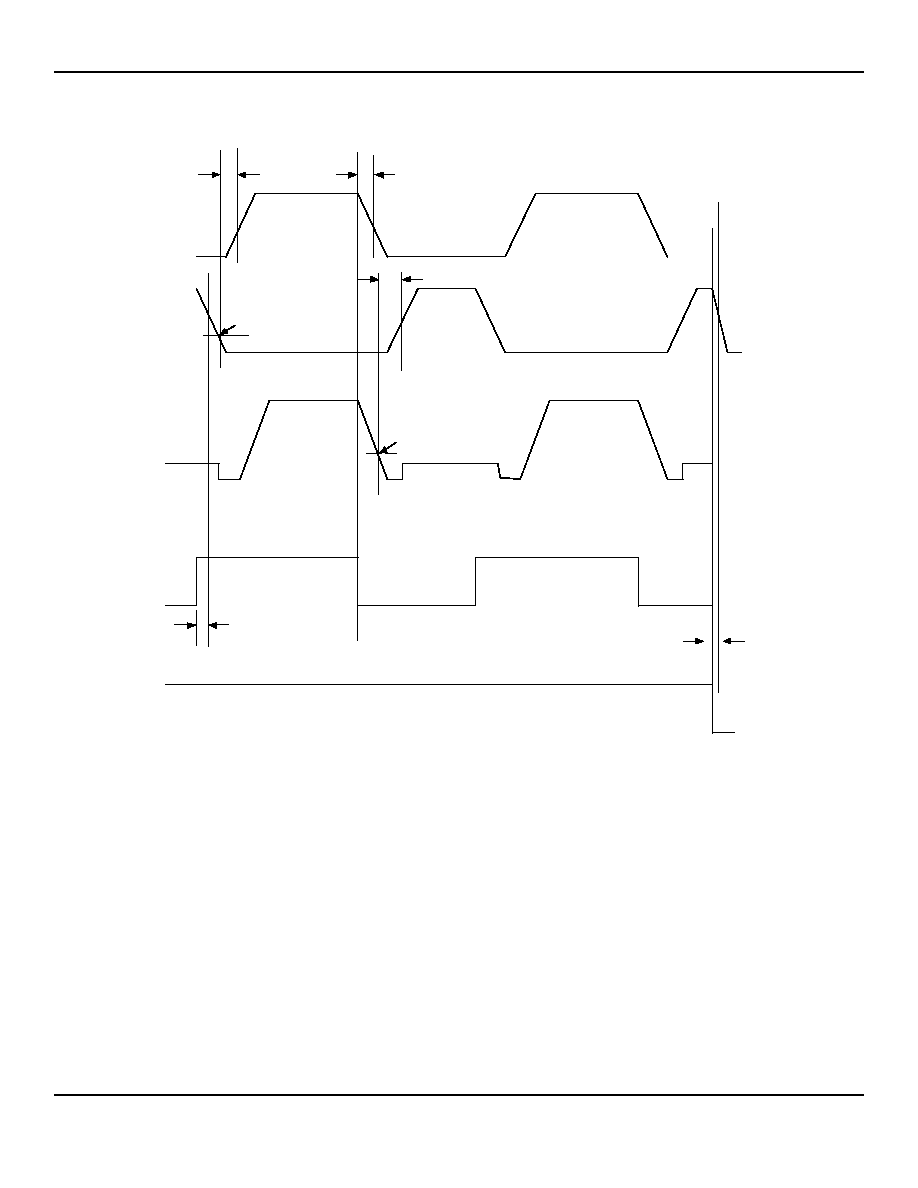
Timing Diagrams
t
LOOFF
30ns
60ns
PWM
LS
Switch node
(HS Pin)
LO
HO
1
2
3. V
LOOFF
<1.7V
4
5
6
7. V
SWth
<(VDD-2.5V)
8
9
10
t
HOON
30ns
60ns
t
HOOFF
45ns
70ns
t
LOON
30ns
70ns
t
LSOFF
36ns
70ns
Time Point
Action
1-2
PWM signal goes high. This initiates the LO signal to go low. The delay between PWM high to (V
LO
≠
10%) is typically 30ns (t
LOOFF
)
2-4
LO goes low. When LO reaches 1.7V (V
LOOFF
) the low side MOSFET is deemed to be off. The high side
output HO then goes high. The delay between 3 and 4 is typically 30ns (T
HOON
); this allows for large turn
off delay times of MOSFETs.
5-7
PWM goes low; HO goes low, typically within 45ns, t
HOOFF
. The switch node (HS pin) is then monitored;
when the switch node is VDD-2.5V (V
SWTH
) the high side MOSFET is deemed to be off and the LO output
goes high within typically 30ns (t
LOON
). This is controlled by a one shot and remains high until PWM goes
high. This is because it is possible to have the SW node oscillate, and could easily bounce through 10V
level. If the LO high transition has not happened within 250ns, it is forced to happen, unless the LS input
is low.
8-10
If at any time after 7 has occurred and LS pin goes low, the LO output will turn off within 36ns (V
LSOFF
).
HO will remain off. The LS pin overrides all shoot through control logic. If LS is low at the start of the next
cycle when PWM signal goes high then HO shall switch transition 1-4 as normal. I.e. PWM signal equals
HO output, LO = 0V.
Micrel, Inc.
MIC4102
October 2004
7
M9999-102004
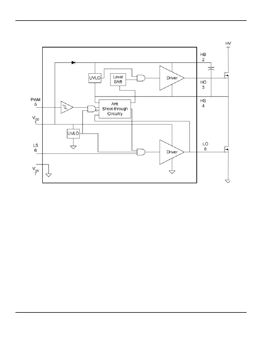
Functional Diagram
MIC4102 Functional Block Diagram

Micrel, Inc.
MIC4102
October 2004
8
M9999-102004
MICREL, INC. 2180 FORTUNE DRIVE SAN JOSE, CA 95131 USA
TEL +1 (408) 944-0800 FAX +1 (408) 474-1000 WEB http:/www.micrel.com
The information furnished by Micrel in this data sheet is believed to be accurate and reliable. However, no responsibility is assumed by Micrel for its
use. Micrel reserves the right to change circuitry and specifications at any time without notification to the customer.
Micrel Products are not designed or authorized for use as components in life support appliances, devices or systems where malfunction of a product
can reasonably be expected to result in personal injury. Life support devices or systems are devices or systems that (a) are intended for surgical implant
into the body or (b) support or sustain life, and whose failure to perform can be reasonably expected to result in a significant injury to the user. A
Purchaser's use or sale of Micrel Products for use in life support appliances, devices or systems is a Purchaser's own risk and Purchaser agrees to fully
indemnify Micrel for any damages resulting from such use or sale.
© 2004 Micrel, Incorporated.