MIC4126/27/28
Dual 1.5A-Peak Low-Side MOSFET
Drivers in Advanced Packaging
MicroLeadFrame and MLF are registered trademarks of Amkor Technology, Inc, Inc.
Micrel, Inc. ∑ 2180 Fortune Drive ∑ San Jose, CA 95131 ∑ USA ∑ tel +1(408) 944-0800 ∑ fax +1(408) 474-1000 ∑ http://www.micrel.com
November 2004
M9999-110304
(408) 955-1690
General Description
The MIC4126, MIC4127, and MIC4128 family are highly-
reliable dual 1.5A low-side MOSFET drivers fabricated on
Micrel's BiCMOS/DMOS process. The devices feature low
power consumption and high efficiency. The
MIC4126/27/28 translate TTL or CMOS input logic levels to
output voltage levels that swing within 25mV of the positive
supply or ground whereas comparable bipolar devices are
capable of swinging only to within 1V of the supply. The
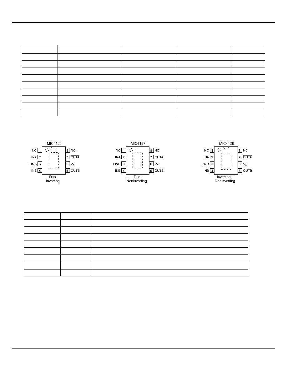
MIC4126/7/8 is available in three configurations: dual
inverting, dual non-inverting, and complimentary output.
The MIC4126/27/28 offer pin-compatible as well as smaller
footprint replacements for the MIC4426/27/28 with
improved packaging and electrical performance. The
MIC4126/27/28 are available in exposed pad, EPAD,
SOIC-8L and MSOP-8L options as well as a small-size
3mm x 3mm MLFTM-8L option. The devices have an input
operating range of 4.5V to 20V.
Primarily intended for driving power MOSFETs,
MIC4426/7/8 drivers are suitable for driving other loads
(capacitive, resistive, or inductive) which require low-
impedance, high peak current, and fast switching time. The
devices can withstand up to 500mA of reverse current
(either polarity) without latching and up to 5V noise spikes
(either polarity) on ground pins.
Data sheets and support documentation can be found on
Micrel's web site at www.micrel.com.
Features
∑ Dual 1.5A-peak drivers
∑ 4.5V to 20V operating range
∑ Exposed backside pad packaging reduces heat
≠ ePAD SOIC-8L (
JA
= 58
∞C/W)
≠ ePAD MSOP-8L (
JA
= 60
∞C/W)
≠ 3mm x 3mm MLFTM-10L (
JA
= 60
∞C/W)
∑ Bipolar/CMOS/DMOS construction
≠ 25mV maximum output offset from supply or ground
∑ Latch-up protection to >500mA reverse current
∑ Switches 1000pF in 25ns
∑ Logic-input threshold independent of supply voltage
∑ Logic-input protection to ≠5V
∑ 6pF typical equivalent input capacitance
∑ Dual inverting, dual non-inverting, and complementary
configurations
∑ -40∞C to +125∞C operating junction temperature range
Applications
∑ DC/DC
converters
∑ Motor drivers
∑ Clock line driver
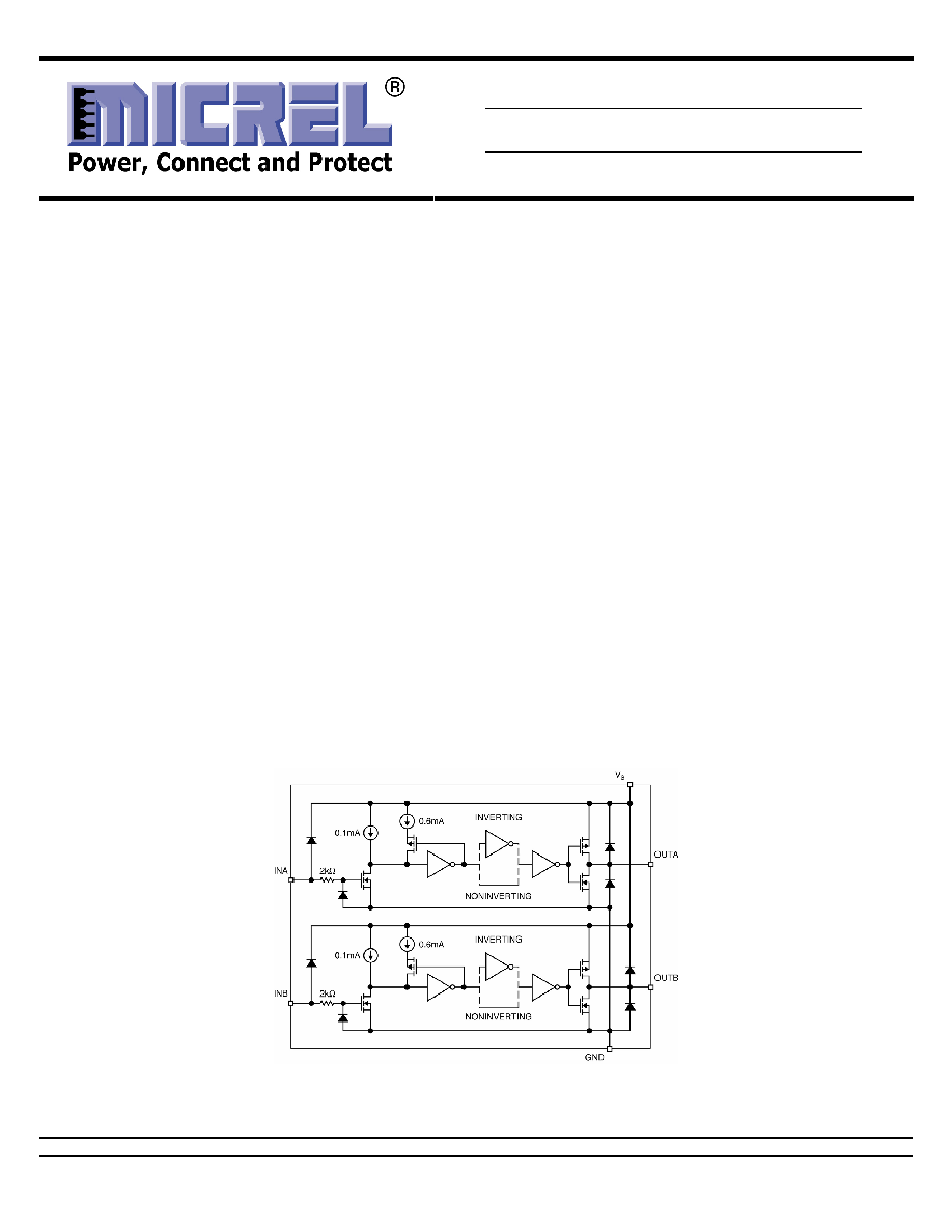
Functional Diagram
MIC4126/27/28 Block Diagram
Micrel
MIC4126/27/28
November 2004
2
M9999-110304
(408) 955-1690
Ordering Information
Part Number
Configuration
Package
Junction Temp. Range
(1)
Lead Finish
MIC4126YME
Dual Inverting
EPAD 8-lead SOIC
≠40∞ to +125∞C
Pb-Free
MIC4126YMME Dual Inverting
EPAD 8-lead MSOP
≠40∞ to +125∞C
Pb-Free
MIC4126YML
Dual Inverting
8-lead MLF
≠40∞ to +125∞C
Pb-Free
MIC4127YME
Dual Non-inverting
EPAD 8-lead SOIC
≠40∞ to +125∞C
Pb-Free
MIC4127YMME Dual Non-inverting
EPAD 8-lead MSOP
≠40∞ to +125∞C
Pb-Free
MIC4127YML
Dual Non-inverting
8-lead MLF
≠40∞ to +125∞C
Pb-Free
MIC4128YME
Inverting + Non-inverting
EPAD 8-lead SOIC
≠40∞ to +125∞C
Pb-Free
MIC4128YMME Inverting + Non-inverting
EPAD 8-lead MSOP
≠40∞ to +125∞C
Pb-Free
MIC4128YML
Inverting + Non-inverting
8-lead MLF
≠40∞ to +125∞C
Pb-Free
Pin Configuration
EPAD SOIC-8L (ME)
EPAD MSOP-8L (MME)
MLF-8L (ML)
EPAD SOIC-8L (ME)
EPAD MSOP-8L (MME)
MLF-8L (ML)
EPAD SOIC-8L (ME)
EPAD MSOP-8L (MME)
MLF-8L (ML)
Pin Description
Pin Number
Pin Name
Pin Function
1, 8
NC
Not internally connected
2
INA
Control Input A: TTL/CMOS compatible logic input
3 GND
Ground
4
INB
Control Input B: TTL/CMOS compatible logic input.
5
OUTB
Output B: CMOS totem-pole output.
6
V
S
Supply Input: +4.5V to +20V
7
OUTA
Output A: CMOS totem-pole output.
EP
GND
Ground, backside pad.
Micrel
MIC4126/27/28
November 2004
3
M9999-110304
(408) 955-1690
Absolute Maximum Ratings
(1)
Supply Voltage (V
S
)......................................................+24V
Input Voltage (V
IN
)...........................V
S
+ 0.3V to GND ≠ 5V
Junction Temperature (T
J
) ......................................... 150∞C
Storage Temperature ................................≠65∞C to +150∞C
Lead Temperature (10 sec.) ...................................... 300∞C
ESD Rating, Note 3
Operating Ratings
(2)
Supply Voltage (V
S
) ...................................... +4.5V to +20V
Temperature Range (T
J
)........................... ≠40∞C to +125∞C
Package Thermal Resistance
3X3
MLFTM
JA
.................................................
60∞C/W
EPAD MSOP-8L
JA
............................... 60∞C/W
EPAD
SOIC-8L
JA
................................. 58∞C/W
Electrical Characteristics
(4)
4.5V V
S
20V; Input voltage slew rate >1V/µs; C
OUT
= 1000pF. T
A
= 25∞C, bold values indicate full specified temperature range;
unless noted.
Symbol Parameter
Condition
Min Typ Max Units
Input
V
IH
Logic 1 Input Voltage
2.4
2.4
1.4
1.6
V
V
IL
Logic 0 Input Voltage
1.1
1.3
0.8
0.8
V
I
IN
Input Current
0 V
IN
V
S
≠1 1 µA
Output
V
OH
High Output Voltage
V
S
≠0.025
V
V
OL
Low Output Voltage
0.025
V
R
O
Output Resistance
I
OUT
= 10mA, V
S
= 18V
6
8
10
12
I
PK
Peak Output Current
1.5 A
I
Latch-Up Protection
Withstand reverse current
>500
mA
Switching Time
t
R
Rise Time
Test Figure 1
13
20
30
40
ns
t
F
Fall Time
Test Figure 1
15
18
25
40
ns
t
D1
Delay Tlme
Test Flgure 1
37
43
50
60
ns
t
D2
Delay Time
Test Figure 1
40
45
60
70
ns
t
PW(min)
Minimum Pulse Width
Test Figure 1
50
ns
Power Supply
I
S
Power Supply Current
V
INA
= V
INB
= 3.0V
1.4
1.5
4.5
8
mA
I
S
Power Supply Current
V
INA
= V
INB
= 0.0V
0.18
0.19
0.4
0.6
mA
Notes:
1. Exceeding the absolute maximum rating may damage the device.
2. The device is not guaranteed to function outside its operating rating.
3. Devices are ESD sensitive. Handling precautions recommended. Human body model: 1.5k
in series with 100pF.
4. Specification for packaged product only.
Micrel
MIC4126/27/28
November 2004
4
M9999-110304
(408) 955-1690
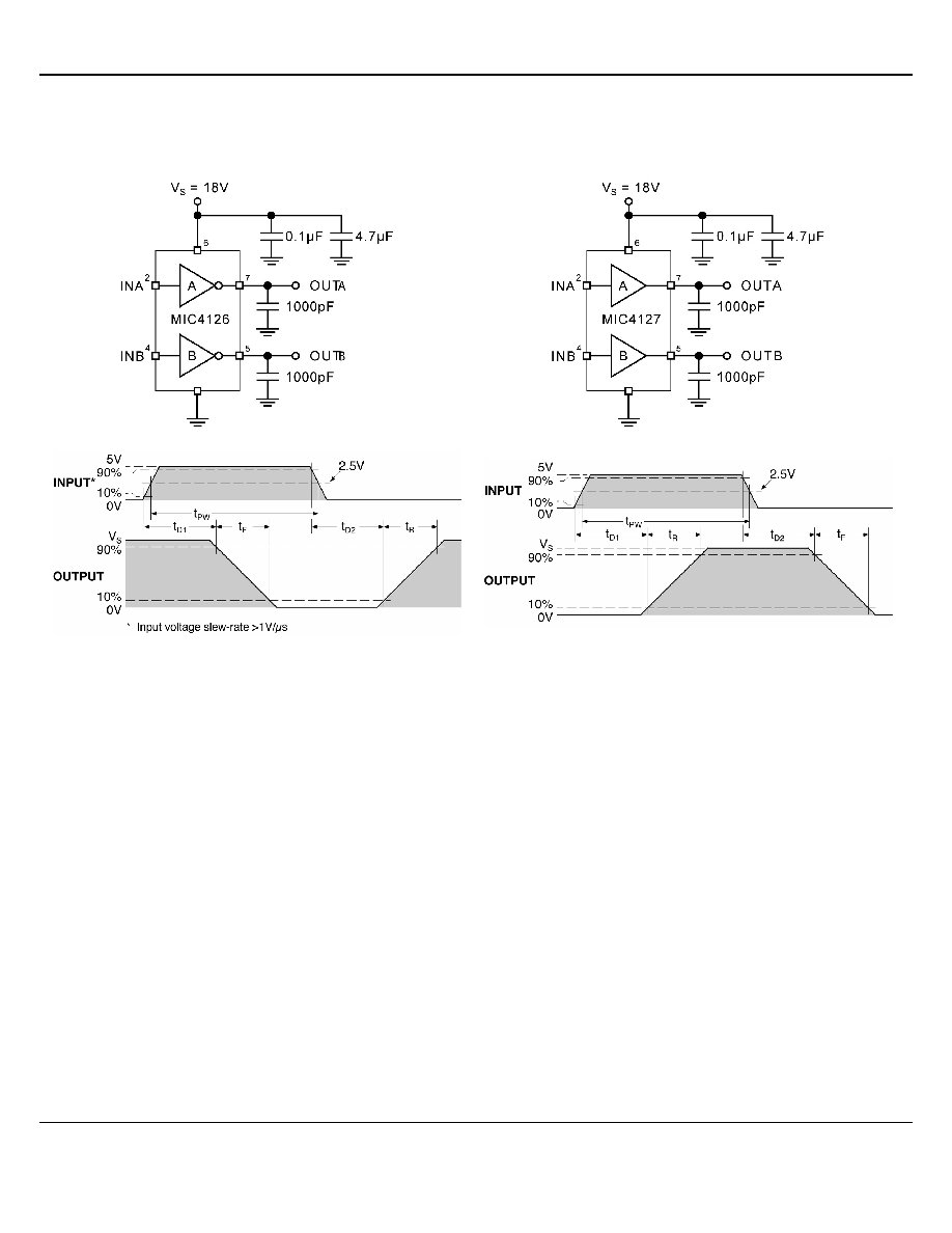
Test Circuit
Figure 1a. Inverting Configuration
Figure 2a. Non-inverting Configuration
Figure 1b. Inverting Timing
Figure 2b. Non-inverting Timing
Micrel
MIC4126/27/28
November 2004
5
M9999-110304
(408) 955-1690
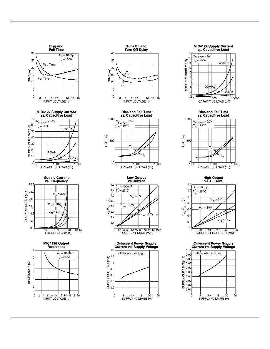
Typical Characteristics
Micrel
MIC4126/27/28
November 2004
6
M9999-110304
(408) 955-1690
Application Information
Supply Bypassing
Large currents are required to charge and discharge large
capacitive loads quickly. For example, changing a 1000pF
load by 16V in 25ns requires 0.8A from the supply input.
To guarantee low supply impedance over a wide frequency
range, parallel capacitors are recommended for power
supply bypassing. Low-inductance ceramic MLC capacitors
with short lead lengths (< 0.5") should be used. A 1.0µF
film capacitor in parallel with one or two 0.1µF ceramic
MLC capacitors normally provides adequate bypassing.
Grounding
When using the inverting drivers in the MIC4126 or
MIC4128, individual ground returns for the input and output
circuits or a ground plane are recommended for optimum
switching speed. The voltage drop that occurs between the
driver's ground and the input signal ground, during normal
high-current switching, will behave as negative feedback
and degrade switching speed.
The E-pad and MLF packages have an exposed pad under
the package. It's important for good thermal performance
that this pad is connected to a ground plane.
Control Input
Unused driver inputs must be connected to logic high
(which can be V
S
) or ground. For the lowest quiescent
current (< 500µA), connect unused inputs-to-ground. A
logic-high signal will cause the driver to draw up to 9mA.
The control input voltage threshold is approximately 1.5V.
The control input recognizes 1.5V up to V
S
as a logic high
and draws less than 1µA within this range.
Power Dissipation
Power dissipation should be calculated to make sure that
the driver is not operated beyond its thermal ratings.
Quiescent power dissipation is negligible. A practical value
for total power dissipation is the sum of the dissipation
caused by the load and the transition power dissipation (P
L
+ P
T
).
Load Dissipation
Power dissipation caused by continuous load current
(when driving a resistive load) through the driver's output
resistance is:
P
L
= I
L
2
R
O
For capacitive loads, the dissipation in the driver is:
P
L
= f C
L
V
S
2
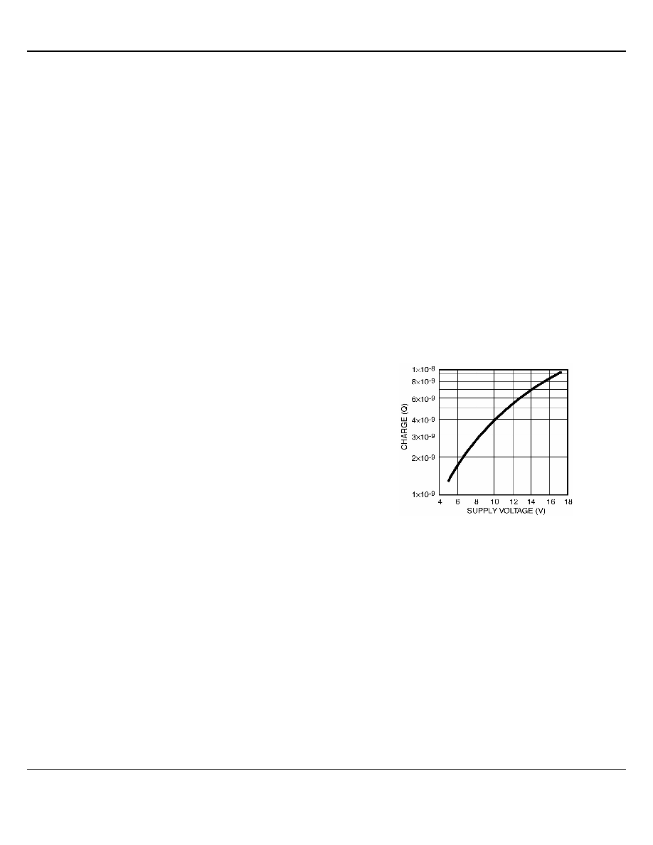
Transition Dissipation
In applications switching at a high frequency, transition
power dissipation can be significant. This occurs during
switching transitions when the P-channel and N-channel
output FETs are both conducting for the brief moment
when one is turning on and the other is turning off.
P
T
= 2 f V
S
Q
Charge (Q) is read from the following graph:
Crossover Energy Loss per Transition
Micrel
MIC4126/27/28
November 2004
7
M9999-110304
(408) 955-1690
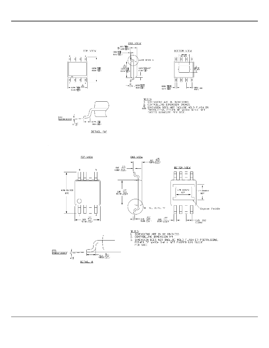
Package Information
8-Pin Exposed Pad SOIC (M)
8-Pin Exposed Pad MSOP (MM)

Micrel
MIC4126/27/28
November 2004
8
M9999-110304
(408) 955-1690
8-Pin MLF (ML)
MICREL, INC. 2180 FORTUNE DRIVE SAN JOSE, CA 95131 USA
TEL +1 (408) 944-0800 FAX +1 (408) 474-1000 WEB http:/www.micrel.com
The information furnished by Micrel in this data sheet is believed to be accurate and reliable. However, no responsibility is assumed by Micrel for its use.
Micrel reserves the right to change circuitry and specifications at any time without notification to the customer.
Micrel Products are not designed or authorized for use as components in life support appliances, devices or systems where malfunction of a product can
reasonably be expected to result in personal injury. Life support devices or systems are devices or systems that (a) are intended for surgical implant into the
body or (b) support or sustain life, and whose failure to perform can be reasonably expected to result in a significant injury to the user. A Purchaser's use or
sale of Micrel Products for use in life support appliances, devices or systems is a Purchaser's own risk and Purchaser agrees to fully indemnify Micrel for any
damages resulting from such use or sale.
© 2004 Micrel, Incorporated.