MIC4421A/4422A
Micrel
October 2002
1
MIC4421A/4422A
MIC4421A/4422A
9A Peak Low-Side MOSFET Driver
Bipolar/CMOS/DMOS Process
General Description
MIC4421A and MIC4422A MOSFET drivers are rugged,
efficient, and easy to use. The MIC4421A is an inverting
driver, while the MIC4422A is a non-inverting driver.
Both versions are capable of 9A (peak) output and can drive
the largest MOSFETs with an improved safe operating mar-
gin. The MIC4421A/4422A accepts any logic input from
2.4V to V
S
without external speed-up capacitors or resistor
networks. Proprietary circuits allow the input to swing nega-
tive by as much as 5V without damaging the part. Additional
circuits protect against damage from electrostatic discharge.
MIC4421A/4422A drivers can replace three or more dis-
crete components, reducing PCB area requirements, simpli-
fying product design, and reducing assembly cost.
Modern Bipolar/CMOS/DMOS construction guarantees free-
dom from latch-up. The rail-to-rail swing capability of CMOS/
DMOS insures adequate gate voltage to the MOSFET dur-
ing power up/down sequencing. Since these devices are
fabricated on a self-aligned process, they have very low
crossover current, run cool, use little power, and are easy to
drive.
Features
∑ High peak-output current: 9A Peak (typ.)
∑ Wide operating range: 4.5V to 18V (typ.)
∑ Minimum pulse width: 50ns
∑ Latch-up proof: fully isolated process is inherently
immune to any latch-up.
∑ Input will withstand negative swing of up to 5V
∑ High capacitive load drive: 47,000pF
∑ Low delay time: 15ns (typ.)
∑ Logic high input for any voltage from 2.4V to V
S
∑ Low equivalent input capacitance (typ.): 7pF
∑ Low supply current: 500
µ
A (typ.)
∑ Output voltage swing to within 25mV of GND or V
S
Applications
∑ Switch mode power supplies
∑ Motor controls
∑ Pulse transformer driver
∑ Class-D switching amplifiers
∑ Line drivers
∑ Driving MOSFET or IGBT parallel chip modules
∑ Local power ON/OFF switch
∑ Pulse generators
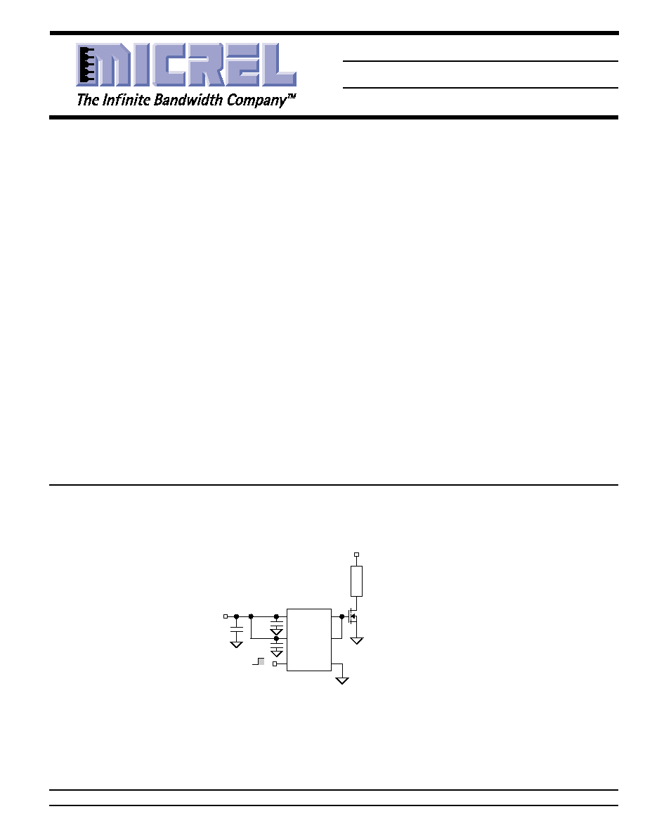
Typical Application
On
Off
VS
OUT
OUT
MIC4421A
1
µ
F
Si9410DY*
N-Channel
MOSFET
Load
Voltage
6
1
7
Load
0.1
µ
F
VS
GND
IN
8
2
4,5
V
S
+15V
0.1
µ
F
* Siliconix 30m
, 7A max.
Load voltage limited by MOSFET drain-to-source rating
Low-Side Power Switch
Micrel, Inc. ∑ 1849 Fortune Drive ∑ San Jose, CA 95131 ∑ USA ∑ tel + 1 (408) 944-0800 ∑ fax + 1 (408) 944-0970 ∑ http://www.micrel.com
MIC4421A/4422A
Micrel
MIC4421A/4422A
2
October 2002
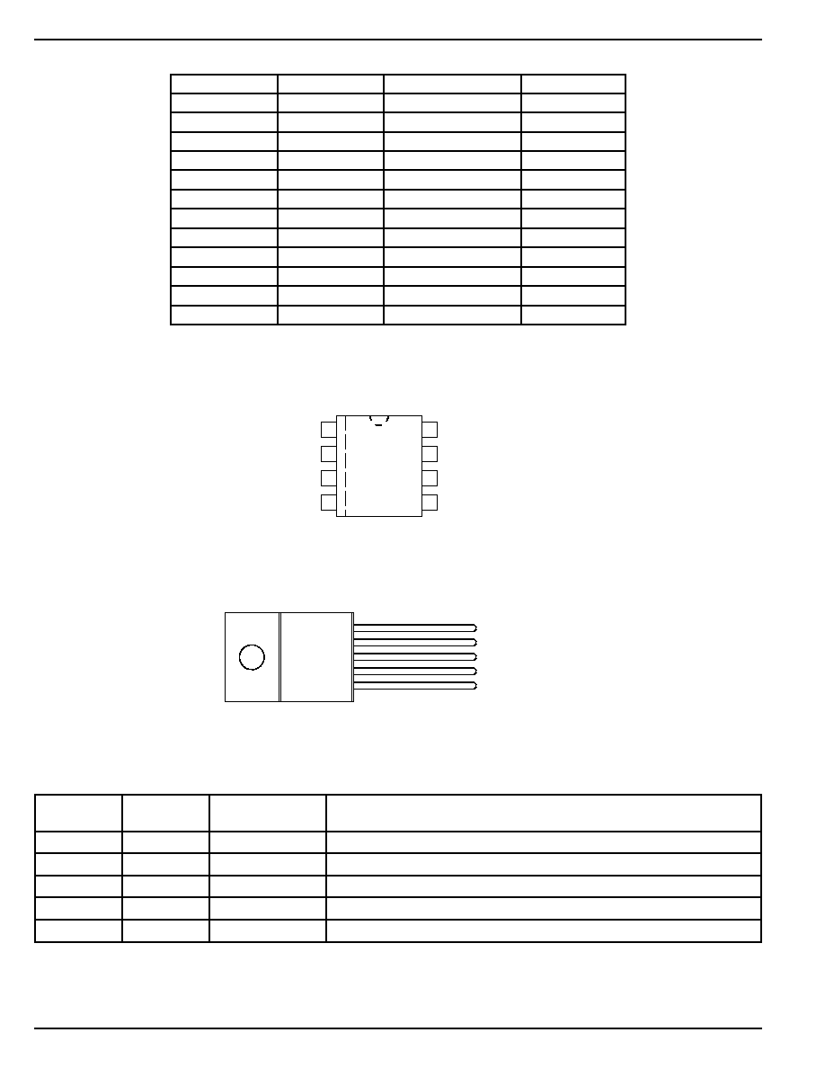
Pin Configurations
1
2
3
4
8
7
6
5
VS
OUT
OUT
GND
VS
IN
NC
GND
Plastic DIP (N)
SOIC (M)
TAB
5
OUT
4
GND
3
VS
2
GND
1
IN
TO-220-5 (T)
Pin Description
Pin Number
Pin Number
Pin Name
Pin Function
TO-220-5
DIP, SOIC
1
2
IN
Control Input.
2, 4
4, 5
GND
Ground: Duplicate pins must be externally connected together.
3,
TAB
1, 8
VS
Supply Input: Duplicate pins must be externally connected together.
5
6, 7
OUT
Output: Duplicate pins must be externally connected together.
3
NC
Not connected.
Ordering Information
Part Number
Configuration
Temperature Range
Package
MIC4421AAM*
Inverting
≠55
∞
C to +125
∞
C
8-Pin SOIC
MIC4421ABM
Inverting
≠40
∞
C to +85
∞
C
8-Pin SOIC
MIC4421ACM
Inverting
0
∞
C to +70
∞
C
8-Pin SOIC
MIC4421ABN
Inverting
≠40
∞
C to +85
∞
C
8-Pin PDIP
MIC4421ACN
Inverting
0
∞
C to +70
∞
C
8-Pin PDIP
MIC4421ACT
Inverting
0
∞
C to +70
∞
C
5-Pin TO-220
MIC4422AAM*
Non-Inverting
≠55
∞
C to +125
∞
C
8-Pin SOIC
MIC4422ABM
Non-Inverting
≠40
∞
C to +85
∞
C
8-Pin SOIC
MIC4422ACM
Non-Inverting
0
∞
C to +70
∞
C
8-Pin SOIC
MIC4422ABN
Non-Inverting
≠40
∞
C to +85
∞
C
8-Pin PDIP
MIC4422ACN
Non-Inverting
0
∞
C to +70
∞
C
8-Pin PDIP
MIC4422ACT
Non-Inverting
0
∞
C to +70
∞
C
5-Pin TO-220
*Special order. Contact factory.

MIC4421A/4422A
Micrel
October 2002
3
MIC4421A/4422A
Electrical Characteristics
T
A
= 25
∞
C with 4.5 V
V
S
18V, bold values indicate ≠55
∞
C
T
A
+125
∞
C; unless noted
Symbol
Parameter
Condition
Min
Typ
Max
Units
Power Supply
V
S
Operating Input Voltage
4.5
18
V
I
S
High Output Quiescent Current
V
IN
= 3V (MIC4422A), V
IN
= 0 (MIC4421A)
0.5
1.5
mA
3
mA
Low Output Quiescent Current
V
IN
= 0V (MIC4422A), V
IN
= 3V (MIC4421A)
50
150
µ
A
200
µ
A
Input
V
IH
Logic 1 Input Voltage
See Figure 3
3.0
2.1
V
V
IL
Logic 0 Input Voltage
See Figure 3
1.5
0.8
V
V
IN
Input Voltage Range
≠5
V
S
+0.3
V
I
IN
Input Current
0 V
V
IN
V
S
≠10
10
µ
A
Output
V
OH
High Output Voltage
See Figure 1
V
S
≠.025
V
V
OL
Low Output Voltage
See Figure 1
0.025
V
R
O
Output Resistance,
I
OUT
= 10 mA, V
S
= 18 V
0.6
1.0
Output High
3.6
R
O
Output Resistance,
I
OUT
= 10 mA, V
S
= 18 V
0.8
1.7
Output Low
2.7
I
PK
Peak Output Current
V
S
= 18 V (See Figure 8)
9
A
I
DC
Continuous Output Current
2
A
I
R
Latch-Up Protection
Duty Cycle
2%
>1500
mA
Withstand Reverse Current
t
300
µ
s, Note 5
Switching Time (Note 5)
t
R
Rise Time
Test Figure 1, C
L
= 10,000 pF
20
75
ns
120
ns
t
F
Fall Time
Test Figure 1, C
L
= 10,000 pF
24
75
ns
120
ns
t
D1
Delay Time
Test Figure 1
15
60
ns
80
ns
t
D2
Delay Time
Test Figure 1
35
60
ns
80
ns
Absolute Maximum Ratings
(Note 1)
Supply Voltage (V
S
) .................................................... +20V
Control Input Voltage (V
IN
) ............. V
S
+ 0.3V to GND ≠ 5V
Control Input Current (V
IN
> V
S
) ............................... 50 mA
Power Dissipation, T
A
25
∞
C, Note 4
PDIP (
JA
) ......................................................... 1478mW
SOIC (
JA
) ........................................................... 767mW
5-Pin TO-220 (
JA
) ............................................ 1756mW
Storage Temperature(T
S
) ........................ ≠65
∞
C to +150
∞
C
Lead Temperature (10 sec) ....................................... 300
∞
C
ESD Rating, Note 3 ...................................................... 2kV
Operating Ratings
(Note 2)
Supply Voltage (V
S
) ..................................... +4.5V to +18V
Ambient Temperature (T
A
) ..................................................
A Version .............................................. ≠55
∞
C to +125
∞
C
B Version ................................................ ≠40
∞
C to +85
∞
C
C Version ................................................... 0
∞
C to +70
∞
C
Junction Temperature (T
J
) ........................................ 150
∞
C
Package Thermal Resistance, Note 4
8-Pin PDIP
(
JA
) ............................................... 84.6
∞
C/W
8-Pin SOIC
(
JA
) ............................................ 163.0
∞
C/W
5-Pin TO-220
(
JA
) ........................................... 71.2
∞
C/W
8-Pin PDIP
(
JC
) ............................................... 41.2
∞
C/W
8-Pin SOIC
(
JC
) .............................................. 38.8
∞
C/W
5-Pin TO-220
(
JC
) ............................................. 6.5
∞
C/W
MIC4421A/4422A
Micrel
MIC4421A/4422A
4
October 2002
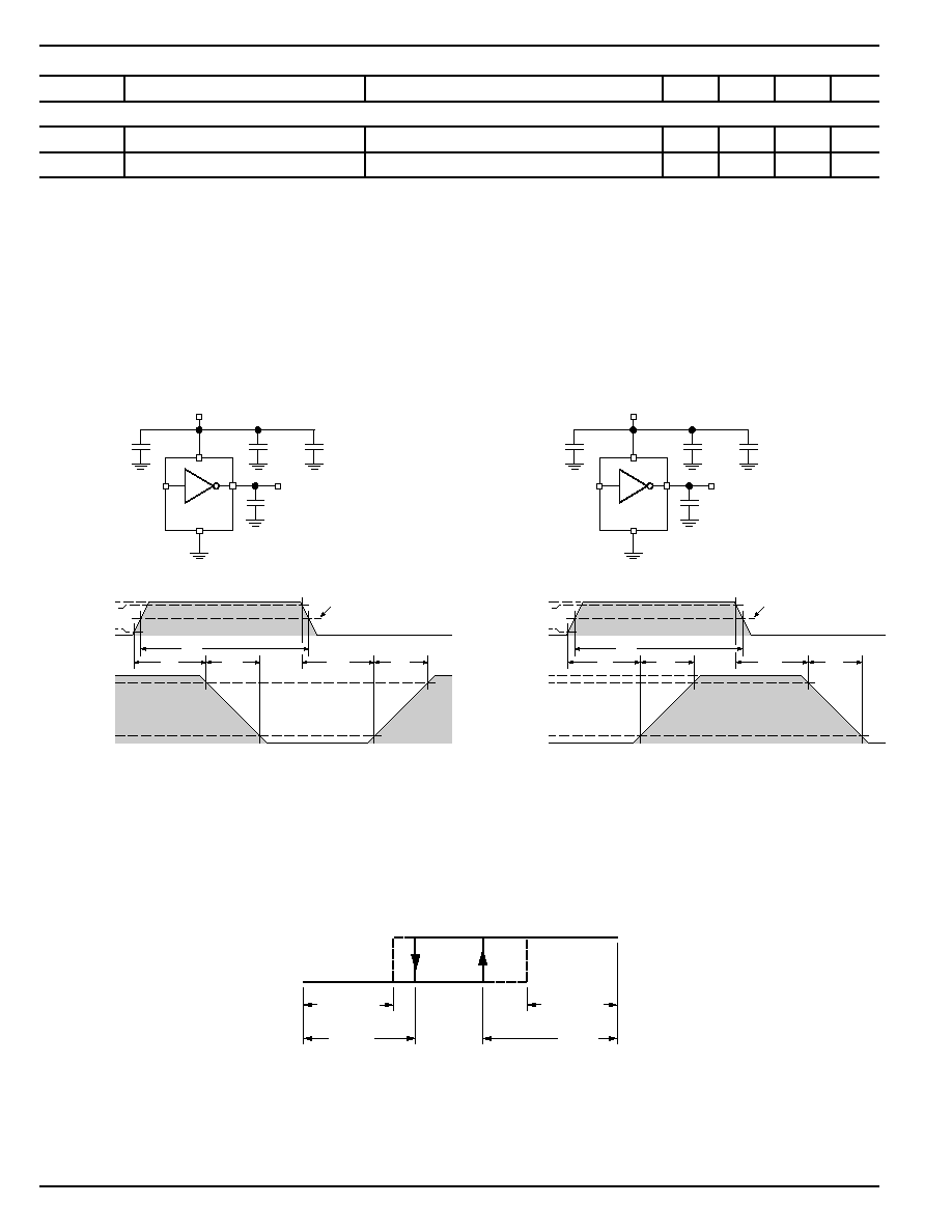
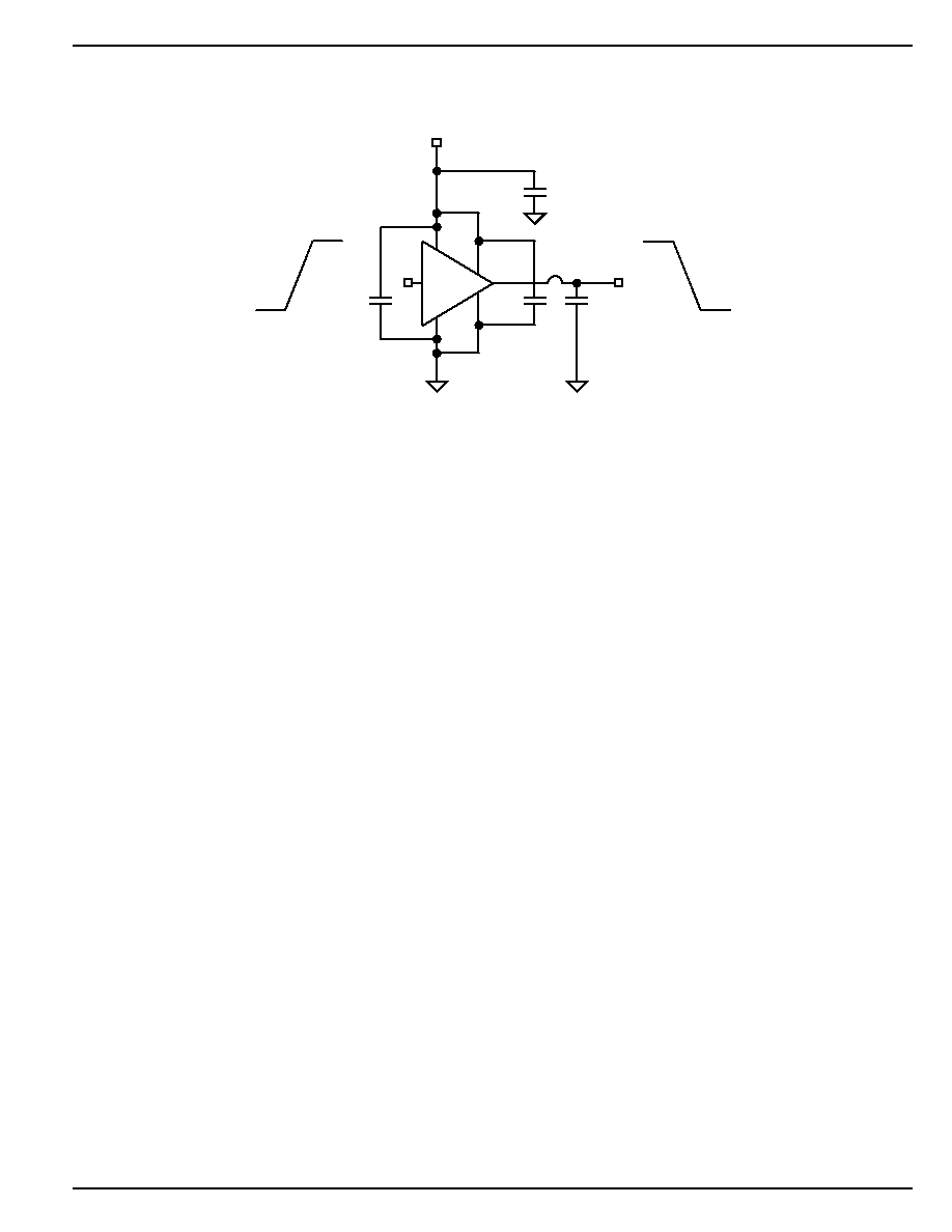
MIC4421A
10,000pF
= 18V
0.1
µ
F
4.7
µ
F
0.1
µ
F
V
IN
V
OUT
V
S
t
D1
90%
10%
t
F
10%
0V
5V
t
D2
t
R
V
S
OUTPUT
INPUT
90%
0V
t
PW
50ns
2.5V
t
PW
Figure 1. Inverting Driver Switching Time
Test Circuits
MIC4422A
10,000pF
= 18V
0.1
µ
F
4.7
µ
F
0.1
µ
F
V
IN
V
OUT
V
S
90%
10%
t
R
10%
0V
5V
t
F
V
S
OUTPUT
INPUT
90%
0V
t
PW
50ns
t
D1
t
D2
t
PW
2.5V
Figure 2. Noninverting Driver Switching Time
Symbol
Parameter
Condition
Min
Typ
Max
Units
Switching Time (Note 5)
t
PW
Minimum Input Pulse Width
See Figure 1. and Figure 2.
50
ns
f
max
Maximum Input Frequency
See Figure 1. and Figure 2.
1
MHz
Note 1.
Exceeding the absolute maximum rating may damage the device.
Note 2.
The device is not guaranteed to function outside its operating rating.
Note 3.
Devices are ESD sensitive. Handling precautions recommended. Human body model, 1.5k in series with 100pF.
Note 4.
Minimum footprint.
Note 5.
Guaranteed by design.
Control Input Behavior
Logic 1
Logic 0
Guaranteed
V
IH
Typical
V
IH
Guaranteed
V
IL
Typical
V
IL
0.8V
1.5V
0V
2.1V
V
S
3V
Figure 3. Input Hysteresis
MIC4421A/4422A
Micrel
October 2002
5
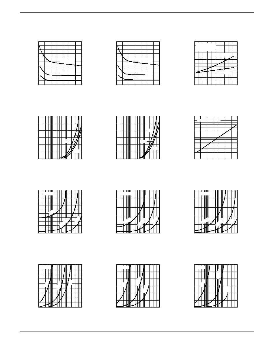
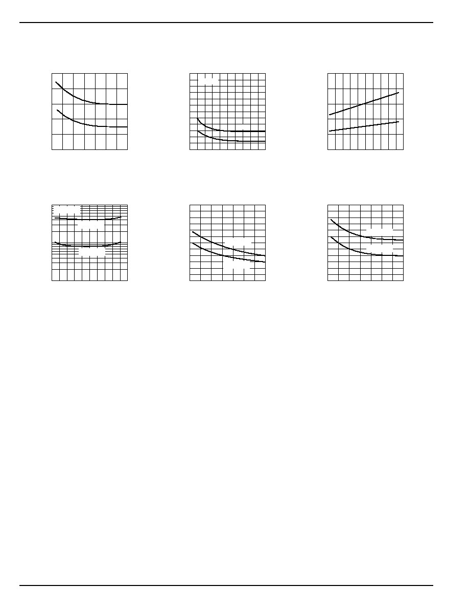
MIC4421A/4422A
4
6
8
10
12
14
16
18
220
200
180
160
140
120
100
80
60
40
0
SUPPLY VOLTAGE (V)
RISE TIME (ns)
Rise Time
vs. Supply Voltage
20
22,000pF
10,000pF
47,000pF
4
6
8
10
12
14
16
18
220
200
180
160
140
120
100
80
60
40
0
SUPPLY VOLTAGE (V)
FALL TIME (ns)
Fall Time
vs. Supply Voltage
20
22,000pF
10,000pF
47,000pF
60
50
40
30
20
10
0
TEMPERATURE (
∞
C)
TIME (ns)
Rise and Fall Times
vs. Temperature
-40
0
40
80
120
C
L
= 10,000pF
V
S
= 18V
t
FALL
t
RISE
100
1000
10k
100k
300
250
200
150
100
50
0
CAPACITIVE LOAD (pF)
RISE TIME (ns)
Rise Time
vs. Capacitive Load
18V
10V
5V
100
1000
10k
100k
300
250
200
150
100
50
0
CAPACITIVE LOAD (pF)
FALL TIME (ns)
Fall Time
vs. Capacitive Load
18V
10V
5V
4
6
8
10
12
14
16
18
10
-7
10
-8
10
-9
VOLTAGE (V)
CROSSOVER ENERGY (A
∑
s)
Crossover Energy
vs. Supply Voltage
PER TRANSITION
100
1000
10k
100k
75
30
0
CAPACITIVE LOAD (pF)
SUPPLY CURRENT (mA)
Supply Current
vs. Capacitive Load
15
45
60
V
S
= 5V
50kHz
1 MHz
200kHz
100
1000
10k
100k
220
160
100
40
0
CAPACITIVE LOAD (pF)
SUPPLY CURRENT (mA)
Supply Current
vs. Capacitive Load
20
60
80
120
140
180
200
V
S
= 18V
50kHz
200kHz
1 MHz
100
1000
10k
100k
150
60
0
CAPACITIVE LOAD (pF)
SUPPLY CURRENT (mA)
Supply Current
vs. Capacitive Load
30
90
120
V
S
= 12V
50kHz
1 MHz
200kHz
Typical Characteristics
10k
100k
1M
10M
120
100
40
0
FREQUENCY (Hz)
SUPPLY CURRENT (mA)
Supply Current
vs. Frequency
20
60
80
V
S
= 12V
0.1µF
0.01µF
1000pF
10k
100k
1M
10M
60
50
20
0
FREQUENCY (Hz)
SUPPLY CURRENT (mA)
Supply Current
vs. Frequency
10
30
40
V
S
= 5V
0.1µF
0.01µF
1000pF
10k
100k
1M
10M
180
160
100
40
0
FREQUENCY (Hz)
SUPPLY CURRENT (mA)
Supply Current
vs. Frequency
20
60
80
120
140
V
S
= 18V
0.1µF
0.01µF
1000pF
MIC4421A/4422A
Micrel
MIC4421A/4422A
6
October 2002
4
6
8
10
12
14
16
18
50
40
30
20
0
SUPPLY VOLTAGE (V)
TIME (ns)
Propagation Delay
vs. Supply Voltage
10
t
D2
t
D1
0
2
4
6
8
10
120
110
100
70
60
50
40
30
20
10
0
INPUT (V)
TIME (ns)
Propagation Delay
vs. Input Amplitude
80
90
t
D2
t
D1
V
S
= 10V
-40
0
40
80
120
1000
100
10
TEMPERATURE (
∞
C)
QUIESCENT SUPPLY CURRENT (µA)
Quiescent Supply Current
vs. Temperature
INPUT = 0
INPUT = 1
V
S
= 18V
4
6
8
10
12
14
16
18
2.4
2.2
2.0
1.4
1.2
1.0
0.8
0.6
0.4
0.2
0
SUPPLY VOLTAGE (V)
HIGH-STATE OUTPUT RESISTANCE (
)
High-State Output Resist.
vs. Supply Voltage
1.6
1.8
T
J
= 25
∞
C
T
J
= 150
∞
C
4
6
8
10
12
14
16
18
2.4
2.2
2.0
1.4
1.2
1.0
0.8
0.6
0.4
0.2
0
SUPPLY VOLTAGE (V)
LOW-STATE OUTPUT RESISTANCE (
)
Low-State Output Resist.
vs. Supply Voltage
1.6
1.8
T
J
= 25
∞
C
T
J
= 150
∞
C
-40
0
40
80
120
50
40
30
20
10
0
TEMPERATURE (
∞
C)
TIME (ns)
Propagation Delay
vs. Temperature
t
D2
t
D1
MIC4421A/4422A
Micrel
October 2002
7
MIC4421A/4422A
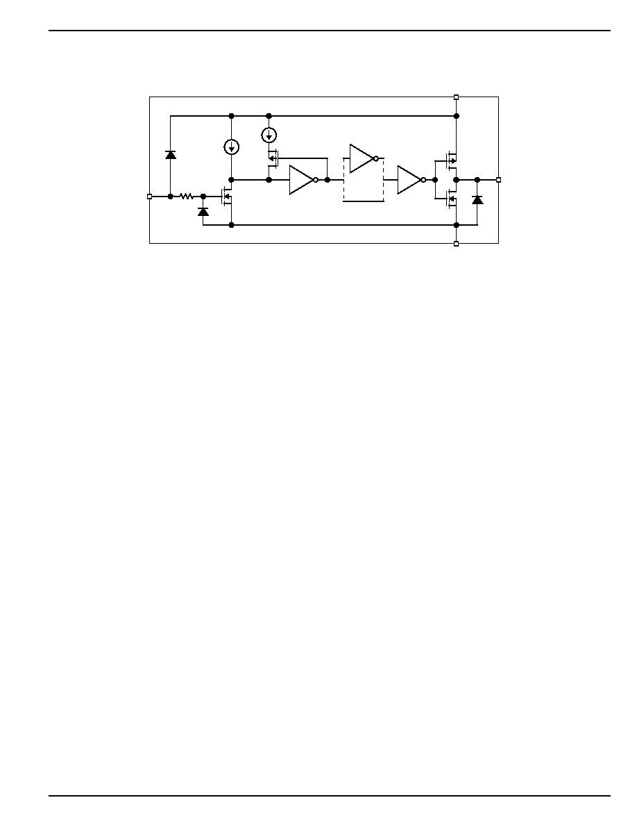
Functional Description
Refer to the functional diagram.
The MIC4422A is a noninverting driver. A logic high on the IN
produces gate drive output. The MIC4421A is an inverting
driver. A logic low on the IN produces gate drive output. The
output is used to turn on an external N-channel MOSFET.
Supply
V
S
(supply) is rated for +4.5V to +18V. External capacitors are
recommended to decouple noise.
Input
IN (control) is a TTL-compatible input. IN must be forced high
or low by an external signal. A floating input will cause
unpredictable operation.
A high input turns on Q1, which sinks the output of the 0.1mA
and the 0.3mA current source, forcing the input of the first
inverter low.
Hysteresis
The control threshold voltage, when IN
is rising, is slightly
higher than the control threshold voltage when CTL is falling.
When IN
is low, Q2 is on, which applies the additional 0.3mA
current source to Q1. Forcing IN
high turns on Q1 which must
sink 0.4mA from the two current sources. The higher current
Functional Diagram
IN
OUT
MIC4421A
INVERTING
MIC4422A
NONINVERTING
0.1mA
0.3mA
2k
V
S
GND
Q2
Q1
Q3
Q4
Figure 4. MIC4421A/22A Block Diagram
through Q1 causes a larger drain-to-source voltage drop
across Q1. A slightly higher control voltage is required to pull
the input of the first inverter down to its threshold.
Q2 turns off after the first inverter output goes high. This
reduces the current through Q1 to 0.1mA. The lower current
reduces the drain-to-source voltage drop across Q1. A slightly
lower control voltage will pull the input of the first inverter up
to its threshold.
Drivers
The second (optional) inverter permits the driver to be manu-
factured in inverting and noninverting versions.
The last inverter functions as a driver for the output MOSFETs
Q3 and Q4.
Output
OUT is designed to drive a capacitive load. V
OUT
(output
voltage) is either approximately the supply voltage or ap-
proximately ground, depending on the logic state applied to
IN.
If IN is high, and V
S
(supply) drops to zero, the output will be
floating (unpredictable).
MIC4421A/4422A
Micrel
MIC4421A/4422A
8
October 2002
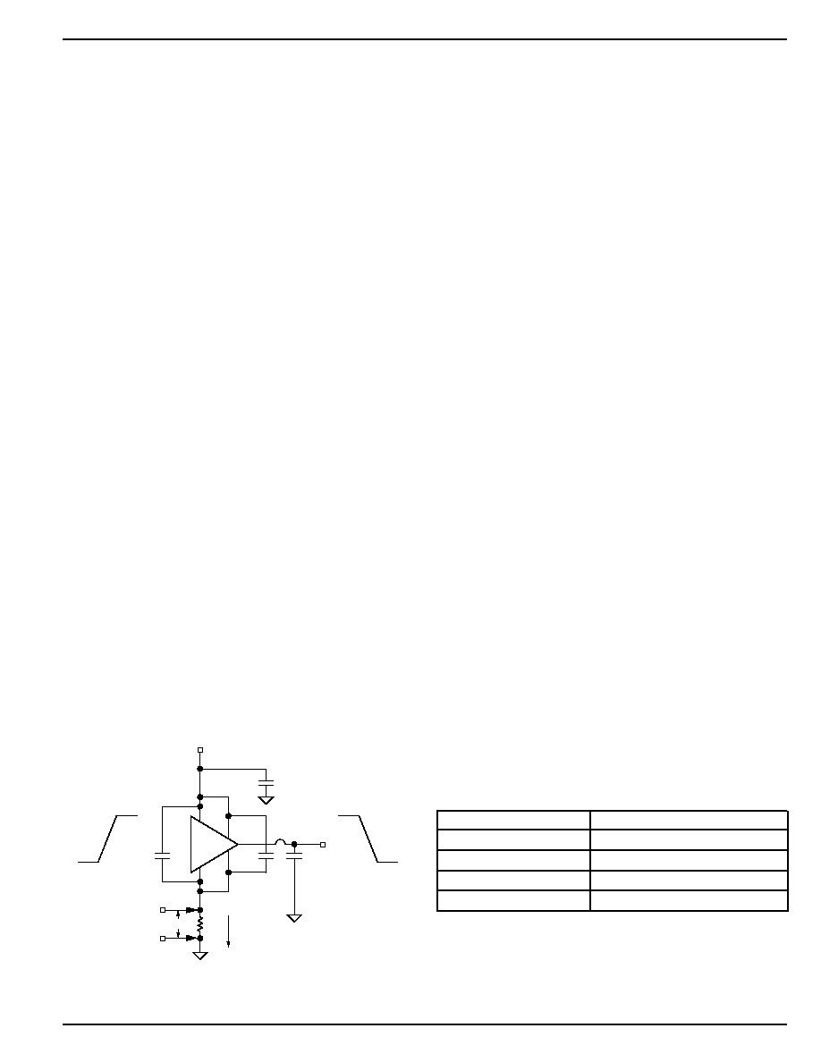
Applications Information
Supply Bypassing
Charging and discharging large capacitive loads quickly
requires large currents. For example, charging a 10,000pF
load to 18V in 50ns requires 3.6A.
The MIC4421A/4422A has double bonding on the supply
pins, the ground pins and output pins. This reduces parasitic
lead inductance. Low inductance enables large currents to be
switched rapidly. It also reduces internal ringing that can
cause voltage breakdown when the driver is operated at or
near the maximum rated voltage.
Internal ringing can also cause output oscillation due to
feedback. This feedback is added to the input signal since it
is referenced to the same ground.
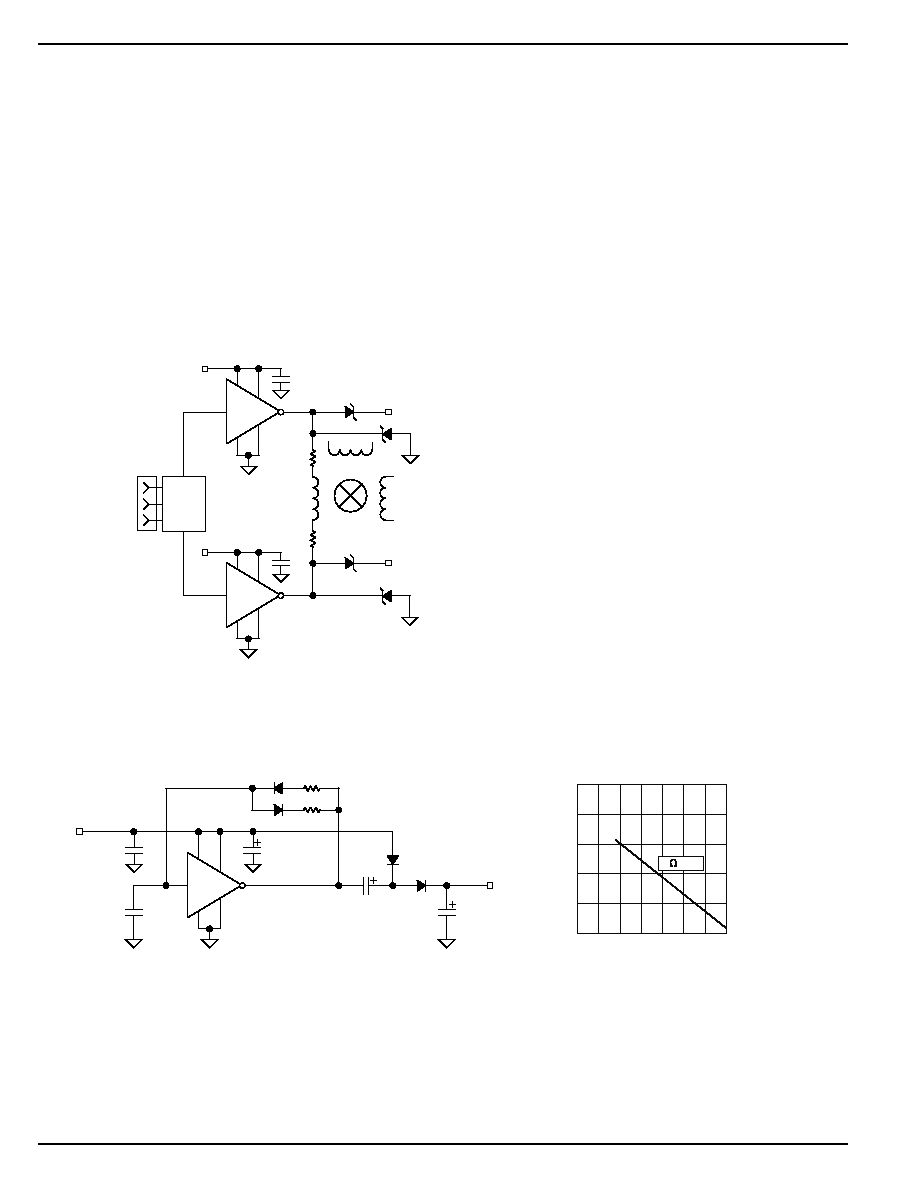
Figure 6. Self Contained Voltage Doubler
30
29
28
27
26
25
mA
VOLTS
Output Voltage
vs. Load Current
0
50 100 150 200 250 300 350
12 LINE
MIC4422A
V
IN
+15V
0.1
µ
F
50V
United Chemcon SXE
0.1
µ
F
WIMA
MKS2
1
µ
F
WIMA
MKS2
BYV 10
(x2)
100
µ
F
50V
500
µ
F
50V
5.6k
560k
1N4448
(x2)
To guarantee low supply impedance over a wide frequency
range, a parallel capacitor combination is recommended for
supply bypassing. Low inductance ceramic disk capacitors
with short lead lengths (< 0.5 inch) should be used. A 1
µ
F low
ESR film capacitor in parallel with two 0.1
µ
F low ESR ceramic
capacitors, (such as AVX RAM Guard
Æ
), provides adequate
bypassing. Connect one ceramic capacitor directly between
pins 1 and 4. Connect the second ceramic capacitor directly
between pins 8 and 5.
Grounding
The high current capability of the MIC4421A/4422A demands
careful PC board layout for best performance. Since the
MIC4421A is an inverting driver, any ground lead impedance
will appear as negative feedback which can degrade switch-
ing speed. Feedback is especially noticeable with slow-rise
time inputs. The MIC4421A input structure includes about
600mV of hysteresis to ensure clean transitions and freedom
from oscillation, but attention to layout is still recommended.
Figure 7 shows the feedback effect in detail. As the MIC4421A
input begins to go positive, the output goes negative and
several amperes of current flow in the ground lead. As little as
0.05
of PC trace resistance can produce hundreds of
millivolts at the MIC4421A ground pins. If the driving logic is
referenced to power ground, the effective logic input level is
reduced and oscillation may result.
To insure optimum performance, separate ground traces
should be provided for the logic and power connections.
Connecting the logic ground directly to the MIC4421A GND
pins will ensure full logic drive to the input and ensure fast
output switching. Both of the MIC4421A GND pins should,
however, still be connected to power ground.
1
µ
F
MIC4421A
Drive
Logic
V
S
V
S
V
S
MIC4422A
V
S
1
µ
F
1 Drive Signal
Conduction Angle
Control 0
∞
C to 180
∞
C
Conduction Angle
Control 180
∞
C to 360
∞
C
1
2
3
Phase 1 of 3 Phase Motor
Driver Using MIC4421A/22A
Figure 5. Direct Motor Drive
MIC4421A/4422A
Micrel
October 2002
9
MIC4421A/4422A
Table 1: MIC4421A Maximum Operating Frequency
V
S
Max Frequency
18V
220kHz
15V
300kHz
10V
640kHz
5V
2MHz
Conditions:
1.
JA
= 150
∞
C/W
2. T
A
= 25
∞
C
3. C
L
= 10,000pF
The supply current vs. frequency and supply current vs.
capacitive load characteristic curves aid in determining
power dissipation calculations. Table 1 lists the maximum
safe operating frequency for several power supply voltages
when driving a 10,000pF load. More accurate power dissi-
pation figures can be obtained by summing the three
dissipation sources.
Given the power dissipation in the device, and the thermal
resistance of the package, junction operating temperature
for any ambient is easy to calculate. For example, the
thermal resistance of the 8-pin plastic DIP package, from
the data sheet, is 84.6
∞
C/W. In a 25
∞
C ambient, then, using
a maximum junction temperature of 150
∞
C, this package
will dissipate 1478mW.
Accurate power dissipation numbers can be obtained by
summing the three sources of power dissipation in the
device:
∑ Load Power Dissipation (P
L
)
∑ Quiescent power dissipation (P
Q
)
∑ Transition power dissipation (P
T
)
Calculation of load power dissipation differs depending on
whether the load is capacitive, resistive or inductive.
Resistive Load Power Dissipation
Dissipation caused by a resistive load can be calculated as:
P
L
= I
2
R
O
D
where:
I =
the current drawn by the load
R
O
= the output resistance of the driver when the
output is high, at the power supply voltage
used. (See data sheet)
D =
fraction of time the load is conducting (duty
cycle).
MIC4421A
V
IN
+18V
0.1
µ
F
1
8
6, 7
5
4
0.1
µ
F
2500pF
Polycarbonate
TEK Current
Probe 6302
Logic
Ground
Power
Ground
300mV
6 Amps
PC Trace
Resistance = 0.05
+18V
0V
+5.0V
0V
WIMA
MKS-2
1
µ
F
Figure 7. Switching Time Degradation Due to
Negative Feedback
Input Stage
The input voltage level of the MIC4421A changes the quies-
cent supply current. The N-Channel MOSFET input stage
transistor drives a 320
µ
A current source load. With a logic "1"
input, the quiescent supply current is typically 500
µ
A. Logic
"0" input level signals reduce quiescent current to 80
µ
A
typical.
The MIC4421A/4422A input is designed to provide 600mV of
hysteresis. This provides clean transitions, reduces noise
sensitivity, and minimizes output stage current spiking when
changing states. Input voltage threshold level is approxi-
mately 1.5V, making the device TTL compatible over the full
temperature and operating supply voltage ranges. Input
current is less than
±
10
µ
A.
The MIC4421A can be directly driven by the TL494, SG1526/
1527, SG1524, TSC170, MIC38C42, and similar switch
mode power supply integrated circuits. By offloading the
power-driving duties to the MIC4421A/4422A, the power
supply controller can operate at lower dissipation. This can
improve performance and reliability.
The input can be greater than the V
S
supply, however, current
will flow into the input lead. The input currents can be as high
as 30mA p-p (6.4mA
RMS
) with the input. No damage will
occur to MIC4421A/4422A however, and it will not latch.
The input appears as a 7pF capacitance and does not change
even if the input is driven from an AC source. While the device
will operate and no damage will occur up to 25V below the
negative rail, input current will increase up to 1mA/V due to
the clamping action of the input, ESD diode, and 1k
resistor.
Power Dissipation
CMOS circuits usually permit the user to ignore power
dissipation. Logic families such as 4000 and 74C have
outputs which can only supply a few milliamperes of current,
and even shorting outputs to ground will not force enough
current to destroy the device. The MIC4421A/4422A on the
other hand, can source or sink several amperes and drive
large capacitive loads at high frequency. The package power
dissipation limit can easily be exceeded. Therefore, some
attention should be given to power dissipation when driving
low impedance loads and/or operating at high frequency.

MIC4421A/4422A
Micrel
MIC4421A/4422A
10
October 2002
Transition Power Dissipation
Transition power is dissipated in the driver each time its
output changes state, because during the transition, for a
very brief interval, both the N- and P-Channel MOSFETs in
the output totem-pole are ON simultaneously, and a current
is conducted through them from V
S
to ground. The transition
power dissipation is approximately:
P
T
= 2 f V
S
(A∑s)
where (A
◊
s) is a time-current factor derived from the typical
characteristic curve "Crossover Energy vs. Supply Voltage."
Total power (P
D
) then, as previously described is just:
P
D
= P
L
+ P
Q
+ P
T
Definitions
C
L
= Load Capacitance in Farads.
D = Duty Cycle expressed as the fraction of time the
input to the driver is high.
f = Operating Frequency of the driver in Hertz.
I
H
= Power supply current drawn by a driver when both
inputs are high and neither output is loaded.
I
L
= Power supply current drawn by a driver when both
inputs are low and neither output is loaded.
I
D
= Output current from a driver in Amps.
P
D
= Total power dissipated in a driver in Watts.
P
L
= Power dissipated in the driver due to the driver's
load in Watts.
P
Q
= Power dissipated in a quiescent driver in Watts.
P
T
= Power dissipated in a driver when the output
changes states ("shoot-through current") in Watts.
NOTE: The "shoot-through" current from a dual
transition (once up, once down) for both drivers is
stated in Figure 7 in ampere-nanoseconds. This
figure must be multiplied by the number of repeti-
tions per second (frequency) to find Watts.
R
O
= Output resistance of a driver in Ohms.
V
S
= Power supply voltage to the IC in Volts.
Capacitive Load Power Dissipation
Dissipation caused by a capacitive load is simply the energy
placed in, or removed from, the load capacitance by the
driver. The energy stored in a capacitor is described by the
equation:
E = 1/2 C V
2
As this energy is lost in the driver each time the load is
charged or discharged, for power dissipation calculations the
1/2 is removed. This equation also shows that it is good
practice not to place more voltage in the capacitor than is
necessary, as dissipation increases as the square of the
voltage applied to the capacitor. For a driver with a capacitive
load:
P
L
= f C (V
S
)
2
where:
f = Operating Frequency
C = Load Capacitance
V
S
= Driver Supply Voltage
Inductive Load Power Dissipation
For inductive loads the situation is more complicated. For the
part of the cycle in which the driver is actively forcing current
into the inductor, the situation is the same as it is in the
resistive case:
P
L1
= I
2
R
O
D
However, in this instance the R
O
required may be either the
on-resistance of the driver when its output is in the high state,
or its on-resistance when the driver is in the low state,
depending on how the inductor is connected, and this is still
only half the story. For the part of the cycle when the inductor
is forcing current through the driver, dissipation is best
described as:
P
L2
= I V
D
(1 ≠ D)
where V
D
is the forward drop of the clamp diode in the driver
(generally around 0.7V). The two parts of the load dissipation
must be summed in to produce P
L
:
P
L
= P
L1
+ P
L2
Quiescent Power Dissipation
Quiescent power dissipation (P
Q
, as described in the input
section) depends on whether the input is high or low. A low
input will result in a maximum current drain (per driver) of
0.2mA; a logic high will result in a current drain of
3.0mA.
Quiescent power can therefore be found from:
P
Q
= V
S
[D I
H
+ (1 ≠ D) I
L
]
where:
I
H
= Quiescent current with input high
I
L
= Quiescent current with input low
D = Fraction of time input is high (duty cycle)
V
S
= Power supply voltage
MIC4421A/4422A
Micrel
October 2002
11
MIC4421A/4422A
MIC4421A
+18V
0.1
µ
F
1
8
6, 7
5
4
0.1
µ
F
10,000pF
Polycarbonate
TEK Current
Probe 6302
+18V
0V
+5.0V
0V
WIMA
MK22
1
µ
F
Figure 8. Peak Output Current Test Circuit
MIC4421A/4422A
Micrel
MIC4421A/4422A
12
October 2002
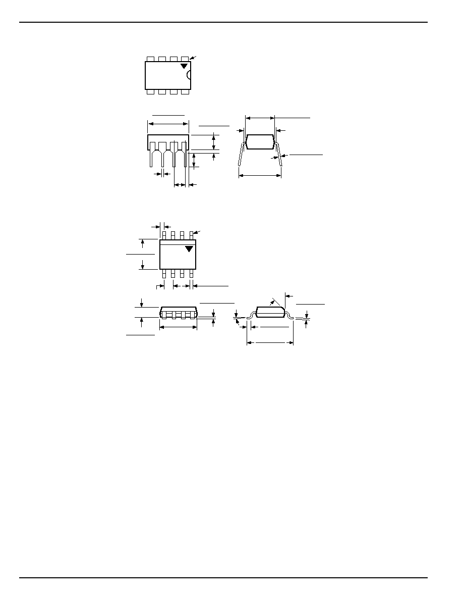
Package Information
0.380 (9.65)
0.370 (9.40)
0.135 (3.43)
0.125 (3.18)
PIN 1
DIMENSIONS:
INCH (MM)
0.018 (0.57)
0.100 (2.54)
0.013 (0.330)
0.010 (0.254)
0.300 (7.62)
0.255 (6.48)
0.245 (6.22)
0.380 (9.65)
0.320 (8.13)
0.0375 (0.952)
0.130 (3.30)
8-Pin Plastic DIP (N)
45
∞
0
∞
≠8
∞
0.244 (6.20)
0.228 (5.79)
0.197 (5.0)
0.189 (4.8)
SEATING
PLANE
0.026 (0.65)
MAX
)
0.010 (0.25)
0.007 (0.18)
0.064 (1.63)
0.045 (1.14)
0.0098 (0.249)
0.0040 (0.102)
0.020 (0.51)
0.013 (0.33)
0.157 (3.99)
0.150 (3.81)
0.050 (1.27)
TYP
PIN 1
DIMENSIONS:
INCHES (MM)
0.050 (1.27)
0.016 (0.40)
8-Pin SOIC (M)
MIC4421A/4422A
Micrel
October 2002
13
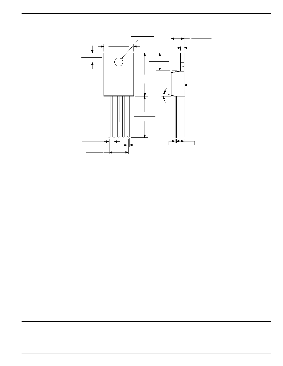
MIC4421A/4422A
0.018
±
0.008
(0.46
±
0.20)
0.268 REF
(6.81 REF)
0.032
±
0.005
(0.81
±
0.13)
0.550
±
0.010
(13.97
±
0.25)
7
∞
Typ.
SEATING
PLANE
0.578
±
0.018
(14.68
±
0.46)
0.108
±
0.005
(2.74
±
0.13)
0.050
±
0.005
(1.27
±
0.13)
0.150 D
±
0.005
(3.81 D
±
0.13)
0.400
±
0.015
(10.16
±
0.38)
0.177
±
0.008
(4.50
±
0.20)
0.103
±
0.013
(2.62
±
0.33)
0.241
±
0.017
(6.12
±
0.43)
0.067
±
0.005
(1.70
±
0.127)
inch
(mm)
Dimensions:
5-Lead TO-220 (T)
MICREL, INC.
1849 FORTUNE DRIVE
SAN JOSE, CA 95131
USA
TEL
+ 1 (408) 944-0800
FAX
+ 1 (408) 944-0970
WEB
http://www.micrel.com
This information is believed to be accurate and reliable, however no responsibility is assumed by Micrel for its use nor for any infringement of patents or
other rights of third parties resulting from its use. No license is granted by implication or otherwise under any patent or patent right of Micrel, Inc.
© 2002 Micrel, Incorporated