 | –≠–ª–µ–∫—Ç—Ä–æ–Ω–Ω—ã–π –∫–æ–º–ø–æ–Ω–µ–Ω—Ç: MIC4680 | –°–∫–∞—á–∞—Ç—å:  PDF PDF  ZIP ZIP |
June 2000
1
MIC4680
MIC4680
Micrel
MIC4680
1A 200kHz SuperSwitcherTM Buck Regulator
Final Information
General Description
The MIC4680 SuperSwitcherTM is an easy-to-use fixed or
adjustable output voltage step-down (buck) switch-mode
voltage regulator. The 200kHz MIC4680 achieves up to 1.3A
of continuous output current over a wide input range in a
8-lead SOP (small outline package).
The MIC4680 is available in 3.3V and 5V fixed output ver-
sions or adjustable output down to 1.25V.
The MIC4680 has an input voltage range of 4V to 34V, with
excellent line, load, and transient response. The regulator
performs cycle-by-cycle current limiting and thermal shut-
down for protection under fault conditions. In shutdown
mode, the regulator draws less than 2
µ
A of standby current.
The MIC4680 SuperSwitcherTM regulator requires a mini-
mum number of external components and can operate using
a standard series of inductors and capacitors. Frequency
compensation is provided internally for fast transient re-
sponse and ease of use.
The MIC4680 is available in the 8-lead SOP with a
≠40
∞
C to +125
∞
C junction temperature range.
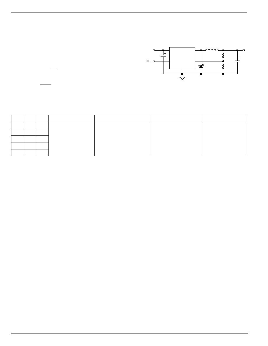
Typical Applications
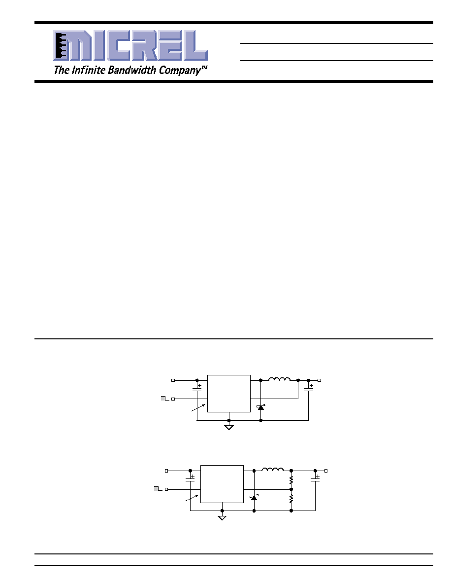
SW
L1
68
µ
H
IN
FB
GND
SHDN
C2
220
µ
F
16V
D1
B260A or
SS26
3.3V/1A
MIC4680-3.3BM
C1
15
µ
F
35V
+6V to +34V
SHUTDOWN
ENABLE
5≠8
4
3
2
1
Power
SOP-8
Fixed Regulator Circuit
SW
L1
68
µ
H
IN
FB
GND
SHDN
C2
220
µ
F
16V
R1
3.01k
R2
2.94k
2.5V/1A
MIC4680BM
C1
15
µ
F
35V
+5V to +34V
SHUTDOWN
ENABLE
Power
SOP-8
5≠8
4
3
2
1
D1
B260A or
SS26
Adjustable Regulator Circuit
Features
∑ SO-8 package with up to 1.3A output current
∑ All surface mount solution
∑ Only 4 external components required
∑ Fixed 200kHz operation
∑ 3.3V, 5V, and adjustable output versions
∑ Internally compensated with fast transient response
∑ Wide 4V to 34V operating input voltage range
∑ Less than 2
µ
A typical shutdown-mode current
∑ Up to 90% efficiency
∑ Thermal shutdown
∑ Overcurrent protection
Applications
∑ Simple 1A high-efficiency step-down (buck) regulator
∑ Replacement of TO-220 and TO-263 designs
∑ Efficient preregulator (5V to 2.5V, 12V to 3.3V, etc.)
∑ On-card switching regulators
∑ Positive-to-negative converter (inverting buck-boost)
∑ Simple battery charger
∑ Negative boost converter
∑ Higher output current regulator using external FET
Micrel, Inc. ∑ 1849 Fortune Drive ∑ San Jose, CA 95131 ∑ USA ∑ tel + 1 (408) 944-0800 ∑ fax + 1 (408) 944-0970 ∑ http://www.micrel.com
SuperSwitcher is a trademark of Micrel, Inc.
MIC4680
Micrel
MIC4680
2
June 2000
Ordering Information
Part Number
Voltage
Junction Temp. Range
Package
MIC4680BM
Adjustable
≠40
∞
C to +125
∞
C
8-lead SOP
MIC4680-3.3BM
3.3V
≠40
∞
C to +125
∞
C
8-lead SOP
MIC4680-5.0BM
5.0V
≠40
∞
C to +125
∞
C
8-lead SOP
Pin Configuration
1
SHDN
IN
SW
FB
8
GND
GND
GND
GND
7
6
5
2
3
4
SOP-8 (M)
Pin Description
Pin Number
Pin Name
Pin Function
1
SHDN
Shutdown (Input): Logic low enables regulator. Logic high (>1.6V) shuts
down regulator.
2
VIN
Supply Voltage (Input): Unregulated +4V to +34V supply voltage.
3
SW
Switch (Output): Emitter of NPN output switch. Connect to external storage
inductor and Shottky diode.
4
FB
Feedback (Input): Connect to output on fixed output voltage versions, or to
1.23V-tap of voltage-divider network for adjustable version.
5≠8
GND
Ground
June 2000
3
MIC4680
MIC4680
Micrel
Electrical Characteristics
V
IN
= 12V; I
LOAD
= 500mA; T
J
= 25
∞
C, bold values indicate ≠40
∞
C
T
J
+125
∞
C, Note 7; unless noted.
Parameter
Condition
Min
Typ
Max
Units
MIC4680 [Adjustable]
Feedback Voltage
(
±
1%)
1.217
1.230
1.243
V
(
±
2%)
1.205
1.255
V
8V
V
IN
34V, 0.1A
I
LOAD
1A, V
OUT
= 5V
1.193
1.230
1.267
V
1.180
1.280
V
Maximum Duty Cycle
V
FB
= 1.0V
93
97
%
Output Leakage Current
V
IN
= 34V, V
SHDN
= 5V, V
SW
= 0V
50
500
µ
A
V
IN
= 34V, V
SHDN
= 5V, V
SW
= ≠1V
4
20
mA
Quiescent Current
V
FB
= 1.5V
7
12
mA
MIC4680-3.3
Output Voltage
(
±
1%)
3.266
3.3
3.333
V
(
±
3%)
3.201
3.399
V
6V
V
IN
34V, 0.1A
I
LOAD
1A
3.168
3.3
3.432
V
3.135
3.465
V
Maximum Duty Cycle
V
FB
= 2.5V
93
97
%
Output Leakage Current
V
IN
= 34V, V
SHDN
= 5V, V
SW
= 0V
50
500
µ
A
V
IN
= 34V, V
SHDN
= 5V, V
SW
= ≠1V
4
20
mA
Quiescent Current
V
FB
= 4.0V
7
12
mA
MIC4680-5.0
Output Voltage
(
±
1%)
4.950
5.0
5.05
V
(
±
3%)
4.85
5.15
V
8V
V
IN
34V, 0.1A
I
LOAD
1A
4.800
5.0
5.200
V
4.750
5.250
V
Maximum Duty Cycle
V
FB
= 4.0V
93
97
%
Output Leakage Current
V
IN
= 34V, V
SHDN
= 5V, V
SW
= 0V
50
500
µ
A
V
IN
= 34V, V
SHDN
= 5V, V
SW
= ≠1V
4
20
mA
Quiescent Current
V
FB
= 6.0V
7
12
mA
Absolute Maximum Ratings
(Note 1)
Supply Voltage (V
IN
), Note 3 ...................................... +38V
Shutdown Voltage (V
SHDN
) .......................... ≠0.3V to +38V
Steady-State Output Switch Voltage (V
SW
) .................. ≠1V
Feedback Voltage [Adjustable] (V
FB
) .......................... +12V
Storage Temperature (T
S
) ....................... ≠65
∞
C to +150
∞
C
ESD, Note 5
Operating Ratings
(Note 2)
Supply Voltage (V
IN
), Note 4 .......................... +4V to +34V
Junction Temperature (T
J
) ...................................... +125
∞
C
Package Thermal Resistance (
JA
), Note 6 ............ 63
∞
C/W
MIC4680
Micrel
MIC4680
4
June 2000
Parameter
Condition
Min
Typ
Max
Units
MIC4680/-3.3/-5.0
Frequency Fold Back
30
50
100
kHz
Oscillator Frequency
180
200
220
kHz
Saturation Voltage
I
OUT
= 1A
1.4
1.8
V
V
Short Circuit Current Limit
V
FB
= 0V, see Test Circuit
1.3
1.8
2.5
A
Standby Quiescent Current
V
SHDN
= V
IN
1.5
µ
A
V
SHDN
= 5V (regulator off)
30
100
µ
A
Shutdown Input Logic Level
regulator off
2
1.6
V
regulator on
1.0
0.8
V
Shutdown Input Current
V
SHDN
= 5V (regulator off)
≠10
≠0.5
10
µ
A
V
SHDN
= 0V (regulator on)
≠10
≠1.5
10
µ
A
Thermal Shutdown
160
∞
C
Note 1.
Exceeding the absolute maximum rating may damage the device.
Note 2.
The device is not guaranteed to function outside its operating rating.
Note 3.
Absolute maximum rating is intended for voltage transients only, prolonged dc operation is not recommended.
Note 4.
V
IN(min)
= V
OUT
+ 2.5V or 4V whichever is greater.
Note 5.
Devices are ESD sensitive. Handling precautions recommended.
Note 6.
Measured on 1" square of 1 oz. copper FR4 printed circuit board connected to the device ground leads.
Note 7.
Test at T
A
= +85
∞
C, guaranteed by design, and characterized to T
J
= +125
∞
C.
Test Circuit
SW
68
µ
H
IN
FB
GND
SHDN
Device Under Test
+12V
SHUTDOWN
ENABLE
SOP-8
5≠8
4
3
2
1
I
Current Limit Test Circuit
Shutdown Input Behavior
OFF
ON
GUARANTEED
OFF
TYPICAL
OFF
GUARANTEED
ON
TYPICAL
ON
0.8V
1V
0V
1.6V
V
IN(max)
2V
Shutodwn Hysteresis
June 2000
5
MIC4680
MIC4680
Micrel
4.96
4.98
5.00
5.02
5.04
0
0.2 0.4 0.6 0.8 1.0 1.2 1.4
OUTPUT VOLTAGE (V)
OUTPUT CURRENT (A)
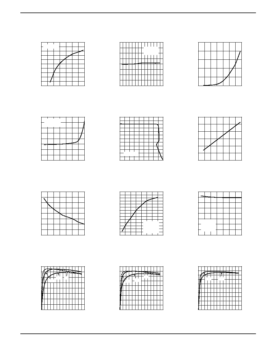
Load Regulation
V
IN
= 12V
V
OUT
= 5V
Typical Characteristics
4.96
4.97
4.98
4.99
5.00
5.01
5.02
5.03
5.04
5.05
5.06
0
5
10
15
20
25
30
35
OUTPUT VOLTAGE (V)
INPUT VOLTAGE (V)
Line Regulation
I
OUT
= 1.0A
0
20
40
60
80
100
0
5
10
15
20
25
30
35
CURRENT (
µ
A)
INPUT VOLTAGE (V)
Shutdown Current
vs. Input Voltage
0
0.5
1.0
1.5
2.0
2.5
3.0
3.5
4.0
-50 -25
0
25
50
75 100 125
CURRENT (
µ
A)
TEMPERATURE (
∞
C)
Shutdown Current
vs. Temperature
V
IN
= 12V
V
SHDN
= V
IN
0
1
2
3
4
5
6
0 0.2 0.4 0.6 0.8 1.0 1.2 1.4 1.6 1.8
OUTPUT VOLTAGE (V)
OUTPUT CURRENT (A)
Current Limit
Characteristic
V
IN
= 12V
196
197
198
199
200
201
202
0
5
10
15
20
25
30
35
FREQUENCY (kHz)
SUPPLY VOLTAGE (V)
Frequency vs.
Supply Voltage
180
190
200
210
220
-50 -25
0
25
50
75 100 125
FREQUENCY (kHz)
TEMPERATURE (
∞
C)
Frequency vs.
Temperature
1.228
1.230
1.232
1.234
1.236
1.238
1.240
1.242
-50 -25 0
25 50 75 100 125 150
FEEDBACK VOLTAGE (V)
TEMPERATURE (
∞
C)
Feedback Voltage
vs. Temperature
V
IN
= 12V
V
OUT
= 5V
I
OUT
= 1A
0
0.2
0.4
0.6
0.8
1.0
1.2
1.4
1.6
-50 -25
0
25
50
75 100 125
SATURATION VOLTAGE (V)
TEMPERATURE (
∞
C)
Saturation Voltage
vs. Temperature
V
IN
= 12V
V
OUT
= 5V
I
LOAD
= 1A
0
10
20
30
40
50
60
70
80
0
0.2 0.4 0.6 0.8 1.0 1.2 1.4
EFFICIENCY (%)
OUTPUT CURRENT (A)
3.3V Output
Efficiency
12V
6V
24V
0
10
20
30
40
50
60
70
80
90
0
0.2 0.4 0.6 0.8 1.0 1.2 1.4
EFFICIENCY (%)
OUTPUT CURRENT (A)
5V Output
Efficiency
7V
12V
24V
0
10
20
30
40
50
60
70
80
90
100
0.0 0.2 0.4 0.6 0.8 1.0 1.2 1.4
EFFICIENCY (%)
OUTPUT CURRENT (A)
12V Output
Efficiency
15V
24V
MIC4680
Micrel
MIC4680
6
June 2000
Switching Frequency Foldback
TIME
Normal
Operation
Short
Circuit
Operation
V
SW
(SHOR
TED)
12V IN, 0V OUT
V
SW
(NORMAL)
12V IN, 5V/1A OUT
200kHz
60kHz
Load Transient
V
IN
= 12V
V
OUT
= 5V
I
OUT
= 1.0A to 0.1A
TIME (100ms/div.)
I
OUT
(500mA/div
.
)
V
OUT
(100mV/div
.
)
5.1V
5V
1A
0A
Functional Characteristics
0
0.1
0.2
0.3
0.4
0.5
0.6
0.7
0.8
0.9
1.0
1.1
1.2
1.3
1.4
1.5
0
5
10
15
20
25
30
35
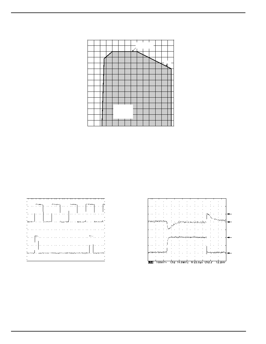
OUTPUT CURRENT (A)
INPUT VOLTAGE (V)
Safe
Operating Area
V
OUT
= 5V
T
A
= 60
∞
C
Demonstration
board layout
Minimum
Current Limit
Note
Frequency Foldback
The MIC4680 folds the switching frequency back during a hard
short-circuit condition to reduce the energy per cycle and
protect the device.
Note. For increased output current, see "Applications Information:
Increasing the Maximum Output Current" and Figure 3.
June 2000
7
MIC4680
MIC4680
Micrel
No-Load Stability
Phase Margin = 125
∞
TIME (100ms/div.)
V
IN
= 34V
V
OUT
= 5.0V
I
OUT
= 1.0A
L = 68
µ
F
C
OUT
= 220
µ
F
Full-Load Stability
Phase Margin = 71
∞
TIME (100ms/div.)
V
IN
= 34V
V
OUT
= 5.0V
I
OUT
= 1.0A
L = 68
µ
F
C
OUT
= 220
µ
F
No-Load Stability
Phase Margin = 106
∞
TIME (100ms/div.)
V
IN
= 7V
V
OUT
= 5.0V
I
OUT
= 0.0A
L = 68
µ
F
C
OUT
= 220
µ
F
Full-Load Stability
Phase Margin = 114
∞
TIME (100ms/div.)
V
IN
= 7V
V
OUT
= 5.0V
I
OUT
= 1.0A
L = 68
µ
F
C
OUT
= 220
µ
F
No-Load Stability
Phase Margin = 117
∞
TIME (100ms/div.)
V
IN
= 12V
V
OUT
= 5.0V
I
OUT
= 0.0A
L = 68
µ
F
C
OUT
= 220
µ
F
Full-Load Stability
Phase Margin = 69
∞
TIME (100ms/div.)
V
IN
= 12V
V
OUT
= 5.0V
I
OUT
= 1.0A
L = 68
µ
F
C
OUT
= 220
µ
F
Bode Plots
The following bode plots show that the MIC4680 is stable over all conditions using a 68
µ
F inductor (L) and a 220
µ
F output
capacitor (C
OUT
). To assure stability, it is a good practice to maintain a phase margin of greater than 35
∞
.
MIC4680
Micrel
MIC4680
8
June 2000
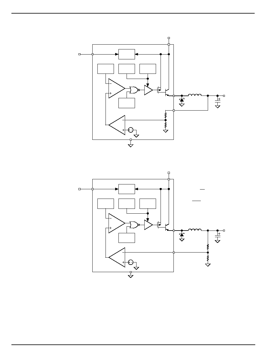
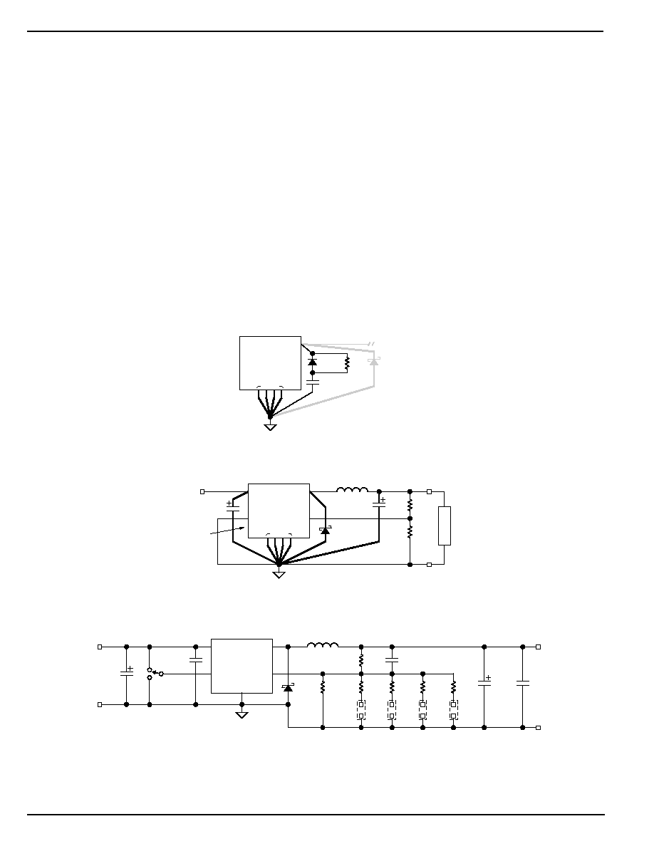
Block Diagrams
SW
GND
FB
C
OUT
V
IN
IN
V
OUT
MIC4680-x.x
Internal
Regulator
SHDN
200kHz
Oscillator
Thermal
Shutdown
Reset
Current
Limit
Com-
parator
Error
Amp
1A
Switch
Driver
1.23V
Bandgap
Reference
Fixed Regulator
SW
FB
R1
R2
C
OUT
V
IN
IN
V
OUT
MIC4680 [adj.]
Internal
Regulator
SHDN
200kHz
Oscillator
Thermal
Shutdown
Reset
Current
Limit
Com-
parator
Error
Amp
1A
Switch
Driver
1.23V
Bandgap
Reference
V
V
R1
R2
1
R1 R2
V
V
1
V
1.23V
OUT
REF
OUT
REF
REF
=
+
=
-
=
Adjustable Regulator

June 2000
9
MIC4680
MIC4680
Micrel
Functional Description
The MIC4680 is a variable duty cycle switch-mode regulator
with an internal power switch. Refer to the block diagrams.
Supply Voltage
The MIC4680 operates from a +4V to +34V unregulated
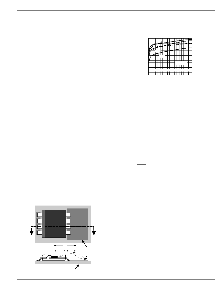
input. Highest efficiency operation is from a supply voltage
around +15V. See the efficiency curves.
Enable/Shutdown
The shutdown (
SHDN
) input is TTL compatible. Ground the
input if unused. A logic-low enables the regulator. A logic-
high shuts down the internal regulator which reduces the
current to typically 1.5
µ
A when V
SHDN
= V
IN
= 12V and 30
µ
A
when V
SHDN
= 5V. See "Shutdown Input Behavior: Shutdown
Hysteresis."
Feedback
Fixed-voltage versions of the regulator have an internal
resistive divider from the feedback (
FB
) pin. Connect
FB
directly to the output voltage.
Adjustable versions require an external resistive voltage
divider from the output voltage to ground, center tapped to the
FB
pin. See Figure 6b for recommended resistor values.
Duty Cycle Control
A fixed-gain error amplifier compares the feedback signal
with a 1.23V bandgap voltage reference. The resulting error
amplifier output voltage is compared to a 200kHz sawtooth
waveform to produce a voltage controlled variable duty cycle
output.
A higher feedback voltage increases the error amplifier
output voltage. A higher error amplifier voltage (comparator
inverting input) causes the comparator to detect only the
peaks of the sawtooth, reducing the duty cycle of the com-
parator output. A lower feedback voltage increases the duty
cycle. The MIC4680 uses a voltage-mode control architec-
ture.
Output Switching
When the internal switch is on, an increasing current flows
from the supply V
IN,
through external storage inductor L1, to
output capacitor C
OUT
and the load. Energy is stored in the
inductor as the current increases with time.
When the internal switch is turned off, the collapse of the
magnetic field in L1 forces current to flow through fast
recovery diode D1, charging C
OUT
.
Output Capacitor
External output capacitor C
OUT
provides stabilization and
reduces ripple. See "Bode Plots" for additional information.
Return Paths
During the on portion of the cycle, the output capacitor and
load currents return to the supply ground. During the off
portion of the cycle, current is being supplied to the output
capacitor and load by storage inductor L1, which means that
D1 is part of the high-current return path.
MIC4680
Micrel
MIC4680
10
June 2000
Applications Information
Adjustable Regulators
Adjustable regulators require a 1.23V feedback signal. Rec-
ommended voltage-divider resistor values for common out-
put voltages are included in Figure 1b.
For other voltages, the resistor values can be determined
using the following formulas:
V
V
R1
R2
1
R1 R2
V
V
1
V
1.23V
OUT
REF
OUT
REF
REF
=
+
=
-
=
SW
L1
IN
FB
GND
SHDN
C
OUT
R1
R2
D1
V
OUT
MIC4680BM
C
IN
V
IN
SHUTDOWN
ENABLE
5≠8
4
3
2
1
Figure 1a. Adjustable Regulator Circuit
V
T
U
O
*
1
R
*
2
R
C
N
I
1
D
1
L
C
T
U
O
V
8
.
1
k
1
0
.
3
k
9
4
.
6
V
5
3
F
µ
5
1
0
0
2
0
R
5
3
0
6
5
1
E
S
P
T
X
V
A
y
k
t
t
o
h
c
S
V
0
6
A
2
*
*
*
.
c
n
I
,
e
d
o
i
D
-
y
a
h
s
i
V
A
0
6
2
B
r
o
r
o
t
c
u
d
n
o
c
i
m
e
S
l
a
r
e
n
e
G
6
2
S
S
A
5
.
1
H
µ
8
6
0
8
6
-
B
2
P
U
s
c
i
n
o
r
t
li
o
C
r
o
*
*
C
M
0
8
6
-
5
2
1
H
R
D
C
a
d
i
m
u
S
r
o
*
*
C
M
0
8
6
-
4
2
1
H
R
D
C
a
d
i
m
u
S
V
0
1
F
µ
0
2
2
0
6
0
0
R
0
1
0
7
2
2
E
S
P
T
X
V
A
V
5
.
2
k
1
0
.
3
k
4
9
.
2
V
3
.
3
k
1
0
.
3
k
8
7
.
1
V
0
.
5
k
1
0
.
3
6
7
9
V
0
.
6
k
1
0
.
3
7
8
7
%
1
s
r
o
t
s
i
s
e
r
ll
A
*
s
n
o
i
t
a
c
il
p
p
a
I
F
R
w
o
l
r
o
f
s
c
i
t
e
n
g
a
m
d
e
d
l
e
i
h
s
*
*
0
0
8
4
-
6
4
4
)
5
0
8
(
.
c
n
I
,
e
d
o
i
D
-
y
a
h
s
i
V
*
*
*
Figure 1b. Recommended Components for Common Ouput Voltages
June 2000
11
MIC4680
MIC4680
Micrel
Minimum Copper/Maximum Current Method
Using Figure 3, for a given input voltage range, determine the
minimum ground-plane heat-sink area required for the
application's maximum output current. Figure 3 assumes a
constant die temperature of 75
∞
C above ambient.
0
0.5
1.0
1.5
0
5
10
15
20
25
OUTPUT CURRENT (I)
AREA (cm
2
)
12V
8V
34V
24V
T
A
= 50
∞
C
Minimum Current Limit = 1.3A
Figure 3. Output Current vs. Ground Plane Area
When designing with the MIC4680, it is a good practice to
connect pins 5 through 8 to the largest ground plane that is
practical for the specific design.
Checking the Maximum Junction Temperature:
For this example, with an output power (P
OUT
) of 5W, (5V
output at 1A maximum with V
IN
= 12V) and 65
∞
C maximum
ambient temperature, what is the maximum junction tem-
perature?
Referring to the "Typical Characteristics: 5V Output Effi-
ciency" graph, read the efficiency (
) for 1A output current at
V
IN
= 12V or perform you own measurement.
= 79%
The efficiency is used to determine how much of the output
power (P
OUT
) is dissipated in the regulator circuit (P
D
).
P =
P
P
D
OUT
OUT
-
P =
5W
0.79
5W
D
-
P
D
= 1.33W
A worst-case rule of thumb is to assume that 80% of the total
output power dissipation is in the MIC4680 (P
D(IC)
) and 20%
is in the diode-inductor-capacitor circuit.
P
D(IC)
= 0.8 P
D
P
D(IC)
= 0.8
◊
1.33W
P
D(IC)
= 1.064W
Calculate the worst-case junction temperature:
T
J
= P
D(IC)
JC
+ (T
C
≠ T
A
) + T
A(max)
where:
T
J
= MIC4680 junction temperature
P
D(IC)
= MIC4680 power dissipation
JC
= junction-to-case thermal resistance.
The
JC
for the MIC4680's power-SOP-8 is
approximately 20
∞
C/W. (Also see Figure 1.)
T
C
= "pin" temperature measurement taken at the
entry point of pins 6 or 7 into the plastic package
JA
JC
CA
AM
BIENT
printed circuit board
ground plane
heat sink area
SOP-8
Figure 2. Power SOP-8 Cross Section
Thermal Considerations
The MIC4680 SuperSwitcher features the power-SOP-8.
This package has a standard 8-lead small-outline package
profile but with much higher power dissipation than a stan-
dard SOP-8. The MIC4680 SuperSwitcher is the first dc-to-dc
converter to take full advantage of this package.
The reason that the power SOP-8 has higher power dissipa-
tion (lower thermal resistance) is that pins 5 though 8 and the
die-attach paddle are a single piece of metal. The die is
attached to the paddle with thermally conductive adhesive.
This provides a low thermal resistance path from the junction
of the die to the ground pins. This design significantly im-
proves package power dissipation by allowing excellent heat
transfer through the ground leads to the printed circuit board.
One of the limitation of the maximum output current on any
MIC4680 design is the junction-to-ambient thermal resis-
tance (
JA
) of the design (package and ground plane).
Examining
JA
in more detail:
JA
= (
JC
+
CA
)
where:
JC
= junction-to-case thermal resistance
CA
= case-to-ambient thermal resistance
JC
is a relatively constant 20
∞
C/W for a power SOP-8.
CA
is dependent on layout and is primarily governed by the
connection of pins 5 though 8 to the ground plane. The
purpose of the ground plane is to function as a heat sink.
JA
is ideally 63
∞
C/W but will vary depending on the size of the
ground plane to which the power SOP-8 is attached.
Determining Ground-Plane Heat-Sink Area
There are two methods of determining the minimum ground
plane area required by the MIC4680.
Quick Method
Make sure that MIC4680 pins 5 though 8 are connected to a
ground plane with a minimum area of 6cm
2
. This ground
plane should be as close to the MIC4680 as possible. The
area maybe disributed in any shape around the package or
on any pcb layer
as long as there is good thermal contact to
pins 5 though 8. This ground plane area is more than
sufficient for most designs.
MIC4680
Micrel
MIC4680
12
June 2000
at the ambient temperature (T
A
) at which T
C
is
measured.
T
A
= ambient temperature at which T
C
is measured.
T
A(max)
= maximum ambient operating temperature
for the specific design.
Calculating the maximum junction temperature given a
maximum ambient temperature of 65
∞
C:
T
J
= 1.064
◊
20
∞
C/W + (45
∞
C ≠ 25
∞
C) + 65
∞
C
T
J
= 106.3
∞
C
This value is less than the allowable maximum operating
junction temperature of 125
∞
C as listed in "Operating Rat-
ings." Typical thermal shutdown is 160
∞
C and is listed in
"Electrical Characteristics."
Increasing the Maximum Output Current
The maximum output current at high input voltages can be
increased for a given board layout. The additional three
components shown in Figure 4 will reduce the overall loss in
the MIC4680 by about 20% at high V
IN
and high I
OUT
.
Even higher output current can be achieved by using the
MIC4680 to switch an external FET. See Figure 9 for a 5A
supply with current limiting.
Layout Considerations
Layout is very important when designing any switching regu-
lator. Rapidly changing switching currents through the printed
circuit board traces and stray inductance can generate volt-
age transients which can cause problems.
To minimize stray inductance and ground loops, keep trace
lengths, indicated by the heavy lines in Figure 5, as short as
possible. For example, keep D1 close to pin 3 and pins 5
through 8, keep L1 away from sensitive node FB, and keep
C
IN
close to pin 2 and pins 5 though 8. See "Applications
Information: Thermal Considerations" for ground plane lay-
out.
The feedback pin should be kept as far way from the switching
elements (usually L1 and D1) as possible.
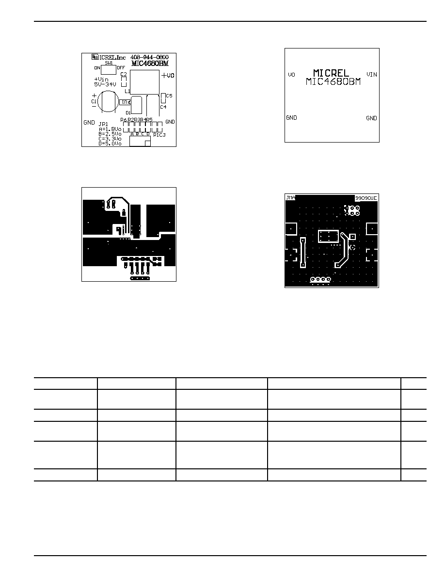
A circuit with sample layouts are provided. See Figure 6a
though 6e.
SW
IN
FB
GND
SHDN
D1
1N4148
2.2nF
82
MIC4680BM
5
6
7
8
3
Figure 4. Increasing Maximum Output Current at High Input Voltages
Load
SW
L1
68
µ
H
IN
FB
GND
SHDN
C
OUT
R1
R2
D1
V
OUT
MIC4680BM
GND
C
IN
V
IN
+4V to +34V
Power
SOP-8
5
6
7
8
4
3
2
1
Figure 5. Critical Traces for Layout
SW
L1
68
µ
H
IN
FB
GND
SHDN
D1
B260A
or
SS26
J2
V
OUT
1A
J4
GND
U1 MIC4680BM
C2
0.1
µ
F
50V
C1
15
µ
F
35V
J1
V
IN
4V to +34V
J3
GND
SOP-8
5≠8
4
3
2
1
S1
NKK G12AP
ON
OFF
C4
220
µ
F
10V
C3*
optional
C5
0.1
µ
F
50V
R1
3.01k
R2
6.49k
JP1a
1.8V
R6
optional
R3
2.94k
R4
1.78k
R5
976
JP1b
2.5V
JP1c
3.3V
JP1d
5.0V
1
2
3
4
5
6
7
8
* C3 can be used to provide additional stability
and improved transient response.
Figure 6a. Evaluation Board Schematic Diagram
June 2000
13
MIC4680
MIC4680
Micrel
Printed Circuit Board Layouts
Figure 6b. Top-Side Silk Screen
Figure 6c. Top-Side Copper
Figure 6d. Bottom-Side Silk Screen
Figure 6e. Bottom-Side Copper
Abbreviated Bill of Material (Critical Components)
Reference
Part Number
Manufacturer
Description
Qty
C1
TPSD156M035R0300
AVX
1
15
µ
F 35V
1
ECE-A1HFS470
Panasonic
2
47
µ
F 50V, 8mm
◊
11.5mm
C4
TPSD227M010R0150
AVX
220
µ
F 10V
1
D1
B260A
Vishay-Diodes, Inc.
3
Schottky
1
SS26
General Semiconductor
L1
UP2B-680
Coiltronics
4
68
µ
H, 1.5A, nonshielded
1
CDH115-680MC
Sumida
5
68
µ
H, 1.5A, nonshielded
CDRH124-680MC
Sumida
5
68
µ
H, 1.5A, shielded
U1
MIC4680BM
Micrel Semiconductor
6
1A 200kHz power-SO-8 buck regulator
1
1
AVX:
http://www.avxcorp.com
2
Panasonic:
http://www.maco.panasonic.co.jp/eccd/index.html
3
Vishay-Diodes, Inc., tel: (805) 446-4800,
http://www.diodes.com
4
Coiltronics, tel: (561) 241-7876,
http://www.coiltronics.com
5
Sumida, tel: (408) 982-9960,
http://www.sumida.com
6
Micrel, tel: (408) 944-0800,
http://www.micrel.com

MIC4680
Micrel
MIC4680
14
June 2000
Applications Circuits*
For continuously updated circuits using the MIC4680, see
Application Hint 37 at www.micrel.com.
SW
L1
100
µ
H
IN
FB
GND
SHDN
C3
220
µ
F
10V
R2
3.01k
R3
976
D2
1N4148
R4
16.2k
R5
221k
R6
10k
U2
R1
0.100
C4
10nF
D1
MMBR140LT3
D3
1N4148
C5
220nF
J2
5V
±
2%
800mA
±
5%
J4
GND
MIC4680BM
C2
100nF
C1
22
µ
F
35V
J1
+34V max.
J3
GND
SOP-8
5≠8
4
3
2
1
S1
NKK G12AP
ON
OFF
LM4041DIM3-1.2
U3
MIC6211BM5
4
5
2
3
R7
4.99k
T
o
Cellular
T
e
lephone
Figure 7. Constant Current and Constant Voltage Battery Charger
SW
L1
33
µ
H
IN
FB
GND
SHDN
C1
68
µ
F
20V
D1
ES1B
1A 100V
J3
GND
U1 MIC4680BM
J4
≠12V/150mA
C2
0.1
µ
F
C4
68
µ
F
20V
C5
33
µ
F
35V
J1
+12V
J2
GND
SOP-8
5≠8
4
3
2
1
R1
8.87k
R2
1k
C3
0.022
µ
F
50V
Figure 8. +12V to ≠12V/150mA Buck-Boost Converter
SW
L1*
50
µ
H
IN
FB
GND
SHDN
C2
220
µ
F
16V
C3
220
µ
F
16V
R7
3.01k
1%
C5
0.1
µ
F
D2
1N4148
R5
16k
1%
R6
16k 1%
C4
1000pF
R2
20m
R3
1k
1%
R4
1k
1%
R8
1.78k
1%
D1
5A
R1
1k
3.3V/5A
GND
U1 MIC4680BM
U2
MIC4417BM4
Si4425DY
C1
330
µ
F
25V
+4.5V to +17V
SHUTDOWN
ENABLE
SOP-8
5≠8
4
3
2
1
* I
SAT
= 8A
U3
MIC6211BM5
Figure 9. 5V to 3.3V/5A Power Supply
* See Application Hint 37 for bills of material.

June 2000
15
MIC4680
MIC4680
Micrel
MIC4680
Micrel
MIC4680
16
June 2000
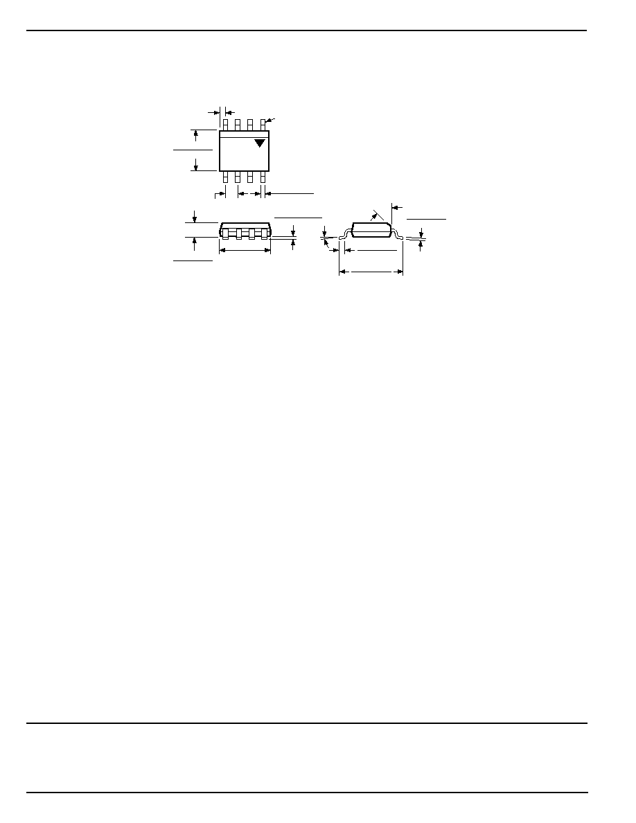
Package Information
45
∞
0
∞
≠8
∞
0.244 (6.20)
0.228 (5.79)
0.197 (5.0)
0.189 (4.8)
SEATING
PLANE
0.026 (0.65)
MAX
)
0.010 (0.25)
0.007 (0.18)
0.064 (1.63)
0.045 (1.14)
0.0098 (0.249)
0.0040 (0.102)
0.020 (0.51)
0.013 (0.33)
0.157 (3.99)
0.150 (3.81)
0.050 (1.27)
TYP
PIN 1
DIMENSIONS:
INCHES (MM)
0.050 (1.27)
0.016 (0.40)
8-Lead SOP (M)
MICREL INC.
1849 FORTUNE DRIVE
SAN JOSE, CA 95131
USA
TEL
+ 1 (408) 944-0800
FAX
+ 1 (408) 944-0970
WEB
http://www.micrel.com
This information is believed to be accurate and reliable, however no responsibility is assumed by Micrel for its use nor for any infringement of patents or
other rights of third parties resulting from its use. No license is granted by implication or otherwise under any patent or patent right of Micrel Inc.
© 2000 Micrel Incorporated