MIC4685
Micrel
September 2002
1
MIC4685
MIC4685
3A SPAK SuperSwitcherTM Buck Regulator
Final
General Description
The MIC4685 is a high-efficiency 200kHz stepdown (buck)
switching regulator. Power conversion efficiency of above
85% is easily obtainable for a wide variety of applications.
The MIC4685 achieves 3A of continuous current in the 7-lead
SPAK package.
The thermal performance of the SPAK allows it to replace
TO-220s and TO-263s (D
2
PAKs) in many applications. The
SPAK saves board space with a 36% smaller footprint than
TO-263.
High efficiency is maintained over a wide output current range
by utilizing a boost capacitor to increase the voltage available
to saturate the internal power switch. As a result of this high
efficiency, only the ground plane of the PCB is needed for a
heat sink.
The MIC4685 allows for a high degree of safety. It has a wide
input voltage range of 4V to 30V (34V transient), allowing it to
be used in applications where input voltage transients may be
present. Built-in safety features include over-current protec-
tion, frequency-foldback short-circuit protection, and thermal
shutdown.
The MIC4685 is available in an 7-lead SPAK package with a
junction temperature range of �40
�
C to +125
�
C.
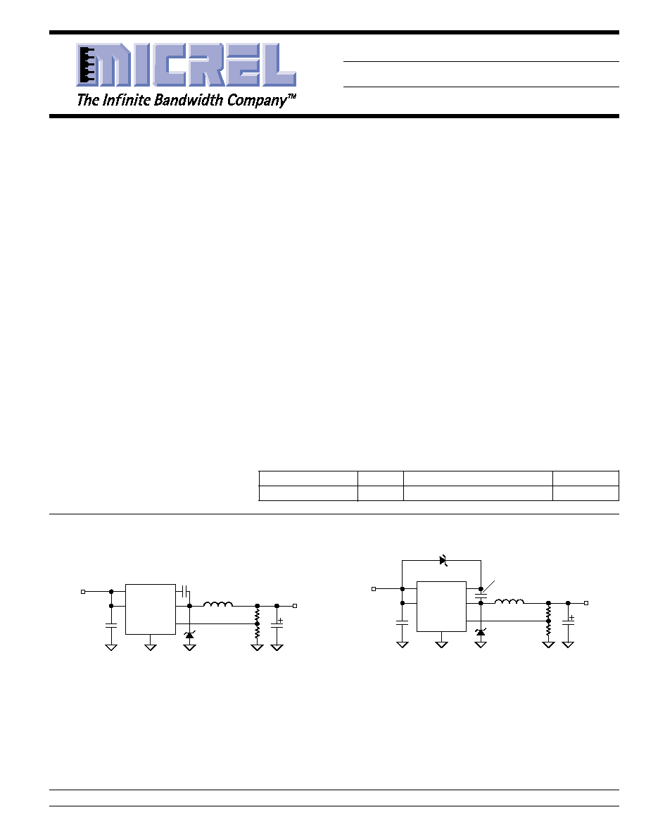
Typical Applications
BS
IN
1
6
3
4, Tab
2
5
SW
FB
EN
GND
MIC4685BR
C
BS
0.33
�
F/50V
C
IN
33
�
F
35V
C
OUT
330
�
F
6.3V
D1
3A
40V
R1
3.01k
R2
6.49k
L1
39
�
H
V
IN
8V to 30V
V
OUT
1.8V/3A
1.8V Output Converter
Features
� Low 2mm profile SPAK package
� 3A continuous output current
� Wide 4V to 30V input voltage range (34V transient)
� Fixed 200kHz PWM operation
� Over 85% efficiency
� Output voltage adjustable to 1.235V
� All surface mount solution
� Internally compensated with fast transient response
� Over-current protection
� Frequency foldback short-circuit protection
� Thermal shutdown
Applications
� Point of load power supplies
� Simple high-efficiency step-down regulators
� 5V to 3.3V/2A conversion
� 12V to 5V/3.3V/2.5V/1.8V 3A conversion
� Dual-output
�
5V conversion
� Base stations
� LCD power supplies
� Battery chargers
Micrel, Inc. � 1849 Fortune Drive � San Jose, CA 95131 � USA � tel + 1 (408) 944-0800 � fax + 1 (408) 944-0970 � http://www.micrel.com
Ordering Information
Part Number
Voltage
Junction Temperature Range
Package
MIC4685BR
Adj
�40
�
C to +125
�
C
SPAK-07L
BS
IN
1
6
3
4, Tab
2
5
SW
FB
EN
GND
D
BS
3A, 20V
MIC4685BR
C
BS
0.33
�
F/50V
C
IN
68
�
F
10V
330
�
F
6.3V
D1
3A
20V
R1
3.01k
R2
1.78k
L1
39
�
H
V
IN
5V
�
10%
V
OUT
3.3V/2A
5V to 3.3V Converter

MIC4685
Micrel
MIC4685
2
September 2002
Pin Description
Pin Number
Pin Name
Pin Function
1
BS
Bootstrap Voltage Node (External Component): Connect to external boost
capacitor.
2
IN
Supply (Input): Unregulated +4V to 30V supply voltage (34V transient)
3
FB
Feedback (Input): Outback voltage feedback to regulator. Connect to 1.235V
tap of resistive divider.
4, Tab
GND
Ground
5
EN
Enable (Input): Logic high = enable; logic low = shutdown
6
SW
Switch (Output): Emitter of NPN output switch. Connect to external storage
inductor and Schottky diode.
7
NC
No Connect. Tie this pin to ground.
Pin Configuration
T
A
B
,
GND
7
NC
6
SW
5
EN
4
GND
3
FB
2
IN
1
BS
SPAK-07L (R)
Detailed Pin Description
Switch (SW, Pin 6)
The switch pin is tied to the emitter of the main internal NPN
transistor. This pin is biased up to the input voltage minus the
V
SAT
of the main NPN pass element. The emitter is also
driven negative when the output inductor's magnetic field
collapses at turn-off. During the OFF time the SW pin is
clamped by the output Schottky diode to a �0.5V typically.
Ground (GND, Pin 4, Tab)
There are two main areas of concern when it comes to the
ground pin, EMI and ground current. In a buck regulator or
any other non-isolated switching regulator the output
capacitor(s) and diode(s) ground is referenced back to the
switching regulator's or controller's ground pin. Any resis-
tance between these reference points causes an offset
voltage/IR drop proportional to load current and poor load
regulation. This is why its important to keep the output
grounds placed as close as possible to the switching regulator's
ground pin. To keep radiated EMI to a minimum it is neces-
sary to place the input capacitor ground lead as close as
possible to the switching regulator's ground pin.
Input Voltage (V
IN
, Pin 2)
The V
IN
pin is the collector of the main NPN pass element.
This pin is also connected to the internal regulator. The output
diode or clamping diode should have its cathode as close as
possible to this point to avoid voltage spikes adding to the
voltage across the collector.
Bootstrap (BS, Pin 1)
The bootstrap pin in conjunction with the external bootstrap
capacitor provides a bias voltage higher than the input
voltage to the MIC4685's main NPN pass element. The
bootstrap capacitor sees the dv/dt of the switching action at
the SW pin as an AC voltage. The bootstrap capacitor then
couples the AC voltage back to the BS pin plus the dc offset
of V
IN
where it is rectified and used to provide additional drive
to the main switch, in this case a NPN transistor.
This additional drive reduces the NPN's saturation voltage
and increases efficiency, from a V
SAT
of 1.8V, and 75%
efficiency to a V
SAT
of 0.5V and 88% efficiency respectively.
Feedback (FB, Pin 3)
The feedback pin is tied to the inverting side of an error
amplifier. The noninverting side is tied to a 1.235V bandgap
reference. An external resistor voltage divider is required
from the output to ground, with the center tied to the feedback
pin.
Enable (EN, Pin 5)
The enable (EN) input is used to turn on the regulator and is
TTL compatible. Note: connect the enable pin to the input if
unused. A logic-high enables the regulator. A logic-low shuts
down the regulator and reduces the stand-by quiescent input
current to typically 150
�
A. The enable pin has an upper
threshold of 2.0V minimum and lower threshold of 0.8V
maximum. The hysterisis provided by the upper and lower
thresholds acts as an UVLO and prevents unwanted turn on
of the regulator due to noise.

MIC4685
Micrel
September 2002
3
MIC4685
Electrical Characteristics
V
IN
= V
EN
=
12V, V
OUT
= 5V; I
OUT
= 500mA; T
A
= 25
�
C, unless otherwise noted. Bold values indicate �40
�
C
T
J
+125
�
C.
Parameter
Condition
Min
Typ
Max
Units
Feedback Voltage
(
�
2%)
1.210
1.235
1.260
V
(
�
3%)
1.198
1.272
V
8V
V
IN
30V, 0.1A
I
LOAD
1A, V
OUT
= 5V, Note 4
1.186
1.235
1.284
V
1.173
1.297
V
Feedback Bias Current
50
nA
Maximum Duty Cycle
V
FB
= 1.0V
94
%
Output Leakage Current
V
IN
= 30V, V
EN
= 0V, V
SW
= 0V
5
500
�
A
V
IN
= 30V, V
EN
= 0V, V
SW
= �1V
1.4
20
mA
Quiescent Current
V
FB
= 1.5V
6
12
mA
Bootstrap Drive Current
V
FB
= 1.5V, V
SW
= 0V
250
380
mA
Bootstrap Voltage
I
BS
= 10mA, V
FB
= 1.5V, V
SW
= 0V
5.5
6.2
V
Frequency Fold Back
V
FB
= 0V
30
70
120
kHz
Oscillator Frequency
180
200
225
kHz
Saturation Voltage
I
OUT
= 1A
0.59
V
Short Circuit Current Limit
V
FB
= 0V, See
Test Circuit
3.5
6
A
Shutdown Current
V
EN
= 0V
150
200
�
A
Enable Input Logic Level
regulator on
2
V
regulator off
0.8
V
Enable Pin Input Current
V
EN
= 0V (regulator off)
16
50
�
A
V
EN
= 12V (regulator on)
�1
�0.83
mA
Thermal Shutdown @ T
J
160
�
C
Note 1.
Exceeding the absolute maximum rating may damage the device.
Note 2.
The device is not guaranteed to function outside its operating rating.
Note 3.
Devices are ESD sensitive. Handling precautions recommended. Human body model, 1.5k
in series with 100pF.
Note 4.
2.5V of headroom is required between V
IN
and V
OUT
. The headroom can be reduced by implementing a bootstrap diode as seen on the 5V to
3.3V circuit on page 1.
Absolute Maximum Ratings
(Note 1)
Supply Voltage (V
IN
), Note 1 ...................................... +34V
Enable Voltage (V
EN
) .................................... �0.3V to +V
IN
Steady-State Output Switch Voltage (V
SW
) ....... �1V to V
IN
Feedback Voltage (V
FB
) .............................................. +12V
Storage Temperature (T
S
) ....................... �65
�
C to +150
�
C
ESD Rating Note 3 ....................................................... 2kV
Operating Ratings
(Note 2)
Supply Voltage (V
IN
) Note 4 ........................... +4V to +30V
Junction Temperature (T
J
) ....................... �40
�
C to +125
�
C
Package Thermal Resistance
JA
, SPAK-7 Lead ............................................ 11.8
�
C/W
JC
, SPAK-7 Lead .............................................. 2.2
�
C/W
MIC4685
Micrel
MIC4685
4
September 2002
Test Circuit
SW
68
�
H
I
VIN
BS
FB
EN
Device Under Test
+12V
3
GND
4, Tab
1
6
2
5
Current Limit Test Circuit
Shutdown Input Behavior
ON
OFF
GUARANTEED
ON
TYPICAL
ON
GUARANTEED
OFF
TYPICAL
OFF
0.8V
1.25V
0V
1.4V
V
IN(max)
2V
Enable Hysteresis
MIC4685
Micrel
September 2002
5
MIC4685
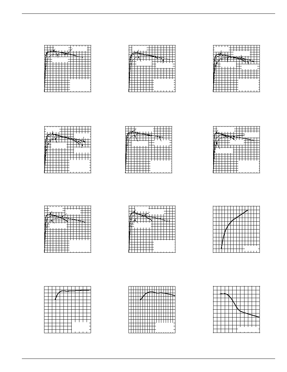
Typical Characteristics
(T
A
= 25
�
C unless otherwise noted)
0
50
100
150
200
250
300
350
0
2
4
6
8 10 12 14 16 18 20
BOOTSTRAP CURRENT (mA)
INPUT VOLTAGE (V)
Bootstrap Drive Current
vs. Input Voltage
V
IN
= 12V
V
FB
= 1.5V
0
1
2
3
4
5
6
7
0
5
10
15
20
25
30
BOOTSTRAP VOLTAGE (V)
INPUT VOLTAGE (V)
Bootstrap Voltage
vs. Input Voltage
V
IN
= 12V
V
FB
= 1.5V
0
10
20
30
40
50
60
70
80
90
100
0 0.5 1.0 1.5 2.0 2.5 3.0 3.5 4.0
EFFICIENCY (%)
OUTPUT CURRENT (A)
Efficiency
vs. Output Current
Standard
Configuration
V
OUT
= 5.0V
V
IN
= 8V
V
IN
= 12V
V
IN
= 30V
0
10
20
30
40
50
60
70
80
90
100
0 0.5 1.0 1.5 2.0 2.5 3.0 3.5 4.0
EFFICIENCY (%)
OUTPUT CURRENT (A)
Efficiency
vs. Output Current
Standard
Configuration
V
OUT
= 3.3V
V
IN
= 8V
V
IN
= 30V
V
IN
= 12V
0
10
20
30
40
50
60
70
80
90
100
0 0.5 1.0 1.5 2.0 2.5 3.0 3.5 4.0
EFFICIENCY (%)
OUTPUT CURRENT (A)
Efficiency
vs. Output Current
Standard
Configuration
V
OUT
= 2.5V
V
IN
= 8V
V
IN
= 30V
V
IN
= 24V
V
IN
= 12V
0
10
20
30
40
50
60
70
80
90
0 0.5 1.0 1.5 2.0 2.5 3.0 3.5 4.0
EFFICIENCY (%)
OUTPUT CURRENT (A)
Efficiency
vs. Output Current
Standard
Configuration
V
OUT
= 1.8V
V
IN
= 8V
V
IN
= 12V
V
IN
= 24V
V
IN
= 30V
0
10
20
30
40
50
60
70
80
90
100
0 0.5 1.0 1.5 2.0 2.5 3.0 3.5 4.0
EFFICIENCY (%)
OUTPUT CURRENT (A)
Efficiency
vs. Output Current
Bootstrap
Configuration
V
OUT
= 5.0V
V
IN
= 7.5V
V
IN
= 12V
V
IN
= 16V
0
10
20
30
40
50
60
70
80
90
100
0 0.5 1.0 1.5 2.0 2.5 3.0 3.5 4.0
EFFICIENCY (%)
OUTPUT CURRENT (A)
Efficiency
vs. Output Current
Bootstrap
Configuration
V
OUT
= 3.3V
V
IN
= 5V
V
IN
= 12V
V
IN
= 16V
V
IN
= 4.5V
0
10
20
30
40
50
60
70
80
90
100
0 0.5 1.0 1.5 2.0 2.5 3.0 3.5 4.0
EFFICIENCY (%)
OUTPUT CURRENT (A)
Efficiency
vs. Output Current
Bootstrap
Configuration
V
OUT
= 2.5V
V
IN
= 5V
V
IN
= 12V
V
IN
= 16V
0
10
20
30
40
50
60
70
80
90
0 0.5 1.0 1.5 2.0 2.5 3.0 3.5 4.0
EFFICIENCY (%)
OUTPUT CURRENT (A)
Efficiency
vs. Output Current
Bootstrap
Configuration
V
OUT
= 1.8V
V
IN
= 5V
V
IN
= 12V
V
IN
= 16V
0
2
4
6
8
10
12
0
5
10
15
20
25
30
DUTY CYCLE (%)
INPUT VOLTAGE (V)
Minimum Duty Cycle
vs. Input Voltage
V
OUT
= 1.8V
5.7
5.8
5.9
6
6.1
6.2
6.3
0
5
10 15 20 25 30 35 40
INPUT CURRENT (mA)
INPUT VOLTAGE (V)
Quiescent Current
vs. Input Voltage
V
EN
= 5V