 | –≠–ª–µ–∫—Ç—Ä–æ–Ω–Ω—ã–π –∫–æ–º–ø–æ–Ω–µ–Ω—Ç: MIC49300 | –°–∫–∞—á–∞—Ç—å:  PDF PDF  ZIP ZIP |
October 2003
1
MIC49300
MIC49300
Micrel
MIC49300
3.0A Low Voltage LDO Regulator w/Dual Input Voltages
General Description
The MIC49300 is a high-bandwidth, low-dropout, 3.0A volt-
age regulator ideal for powering core voltages of low-power
microprocessors. The MIC49300 implements a dual supply
configuration allowing for very low output impedance and
very fast transient response.
The MIC49300 requires a bias input supply and a main input
supply, allowing for ultra-low input voltages on the main
supply rail. The input supply operates from 1.4V to 6.5V and
the bias supply requires between 3V and 6.5V for proper
operation. The MIC49300 offers fixed output voltages from
0.9V to 1.8V and adjustable output voltages down to 0.9V.
The MIC49300 requires a minimum of output capacitance for
stability, working optimally with small ceramic capacitors.
The MIC49300 is available in a 5-pin S-Pak. It operates over
a junction temperature range of ≠40
∞
C to +125
∞
C.
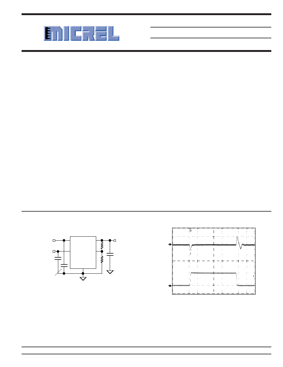
Typical Application
MIC49300BR
GND
C
OUT
=
10
µ
F
Ceramic
BIAS
IN
OUT
C
BIAS
= 1
µ
F
Ceramic
V
OUT
= 1.0V
V
IN
= 1.5V
V
BIAS
= 3.3V
ADJ
C
IN
= 1
µ
F
Ceramic
R1
R2
Low Voltage,
Fast Transient Response Regulator
Micrel, Inc. ∑ 1849 Fortune Drive ∑ San Jose, CA 95131 ∑ USA ∑ tel + 1 (408) 944-0800 ∑ fax + 1 (408) 944-0970 ∑ http://www.micrel.com
Load Transient Response
TIME (20
µ
s/div.)
V
OUT
20mV/div
I
OUT
2A/div
V
BIAS
= 5V
V
IN
= 2.5V
V
OUT
= 1.8V
C
OUT
= 10
µ
F Ceramic
Features
∑ Input Voltage Range:
V
IN
: 1.4V to 6.5V
V
BIAS
: 3.0V to 6.5V
∑ Stable with 1
µ
F ceramic capacitor
∑
±
1% initial tolerance
∑ Maximum dropout voltage (V
IN
-V
OUT
) of 500mV over
temperature
∑ Adjustable output voltage down to 0.9V
∑ Ultra fast transient response (Up to 10MHz bandwidth)
∑ Excellent line and load regulation specifications
∑ Logic controlled shutdown option
∑ Thermal shutdown and current limit protection
∑ Power S-Pak package
∑ Junction temperature range: ≠40
∞
C to 125
∞
C
Applications
∑ Graphics processors
∑ PC Add-In Cards
∑ Microprocessor core voltage supply
∑ Low voltage digital ICs
∑ High Efficiency Linear power supplies
∑ SMPS post regulators
MIC49300
Micrel
MIC49300
2
October 2003
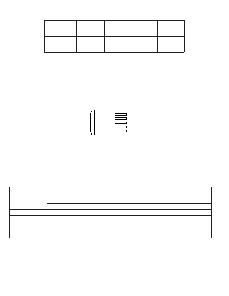
Pin Configuration
TA
B
5 VOUT
4
VBIAS
3
2
VIN
1 EN/ADJ.
GND
5-Lead S-Pak (R)
Pin Description
Pin Number
Pin Name
Pin Function
1
Enable
Enable (Input): CMOS compatible input. Logic high = enable, logic low =
shutdown.
ADJ.
Adjustable regulator feedback input. Connect to resistor voltage divider.
4
VIN
Input voltage which supplies current to the output power device.
5
VOUT
Regulator Output.
2
VBIAS
Input Bias Voltage for powering all circuitry on the regulator with the excep-
tion of the output power device.
3
GND
Ground (TAB is connected to ground on S-Pak).
Ordering Information
Part Number
Output Current
Voltage
Temperature Range
Package
MIC49300-0.9BR
3A
0.9V
≠40
∞
C to +125
∞
C
S-Pak-5
MIC49300-1.2BR
3A
1.2V
≠40
∞
C to +125
∞
C
S-Pak-5
MIC49300-1.5BR
3A
1.5V
≠40
∞
C to +125
∞
C
S-Pak-5
MIC49300-1.8BR
3A
1.8V
≠40
∞
C to +125
∞
C
S-Pak-5
MIC49300BR
3A
ADJ.
≠40
∞
C to +125
∞
C
S-Pak-5
Other voltages available. Contact Micrel for details.
October 2003
3
MIC49300
MIC49300
Micrel
Electrical Characteristics
T
A
= 25
∞
C with V
BIAS
= V
OUT
+2.1V; V
IN
= V
OUT
+ 1V; bold values indicate ≠40
∞
C < T
J
< +125
∞
C, Note 4; unless otherwise specified.
Parameter
Conditions
Min
Typ
Max
Units
Output Voltage Accuracy
At 25
∞
C, fixed voltage options
≠1
+1
%
Over temperature range
≠2
+2
%
Line Regulation
V
IN
= 2.0V to 6.5V
≠0.1
0.01
+0.1
%/V
Load Regulation
I
L
= 0mA to 3A
0.2
0.5
%
Dropout Voltage (V
IN
≠ V
OUT
)
I
L
= 1.5A
125
200
mV
I
L
= 3A
280
400
mV
Dropout Voltage (V
BIAS
≠ V
OUT
)
I
L
= 3A
1.5
2.1
V
Note 4
Ground Pin Current, Note 5
I
L
= 0mA
25
mA
I
L
= 3A
25
50
mA
Ground Pin Current in Shutdown
V
EN
0.6V, (I
BIAS
+ I
CC
), Note 6
0.07
5
µ
A
Current thru V
BIAS
I
L
= 0mA
20
35
mA
I
L
= 3A
50
150
mA
Current Limit
V
OUT
= 0V
6.5
9
A
Enable Input, Note 6
Enable Input Threshold
Regulator enable
1.6
V
(Fixed Voltage only)
Regulator shutdown
0.6
V
Enable Pin Input Current
0.1
1.0
µ
A
Reference
Reference Voltage
Adjustable option only
0.891
0.9
0.909
V
0.882
0.918
V
Note 1.
Exceeding the absolute maximum rating may damage the device.
Note 2.
The device is not guaranteed to function outside its operating rating.
Note 3.
Devices are ESD sensitive. Handling precautions recommended. Human body model, 1.5k in series with 100pF.
Note 4.
For V
OUT
1V, V
BIAS
dropout specification does not apply due to a minimum 3V V
BIAS
input.
Note 5.
I
GND
= I
BIAS
+ (I
IN
≠ I
OUT
). At high loads, input current on V
IN
will be less than the output current, due to drive current being supplied by V
BIAS
.
Note 6.
Fixed output voltage versions only.
Absolute Maximum Ratings
(Note 1)
Supply Voltage (V
IN
) ....................................................... 8V
Bias Supply Voltage (V
BIAS
) ............................................ 8V
Enable Input Voltage (V
EN
) ............................................. 8V
Power Dissipation .................................... Internally Limited
ESD Rating, Note 3 ...................................................... 2kV
Operating Ratings
(Note 2)
Supply Voltage (V
IN
) ....................................... 1.4V to 6.5V
Bias Supply Voltage (V
BIAS
) ............................... 3V to 6.5V
Enable Input Voltage (V
EN
) .................................. 0V to V
IN
Junction Temperature Range ............. ≠40
∞
C
T
J
+125
∞
C
Package Thermal Resistance
S-PAK
(
JC
) ............................................................ 2
∞
C/W
MIC49300
Micrel
MIC49300
4
October 2003
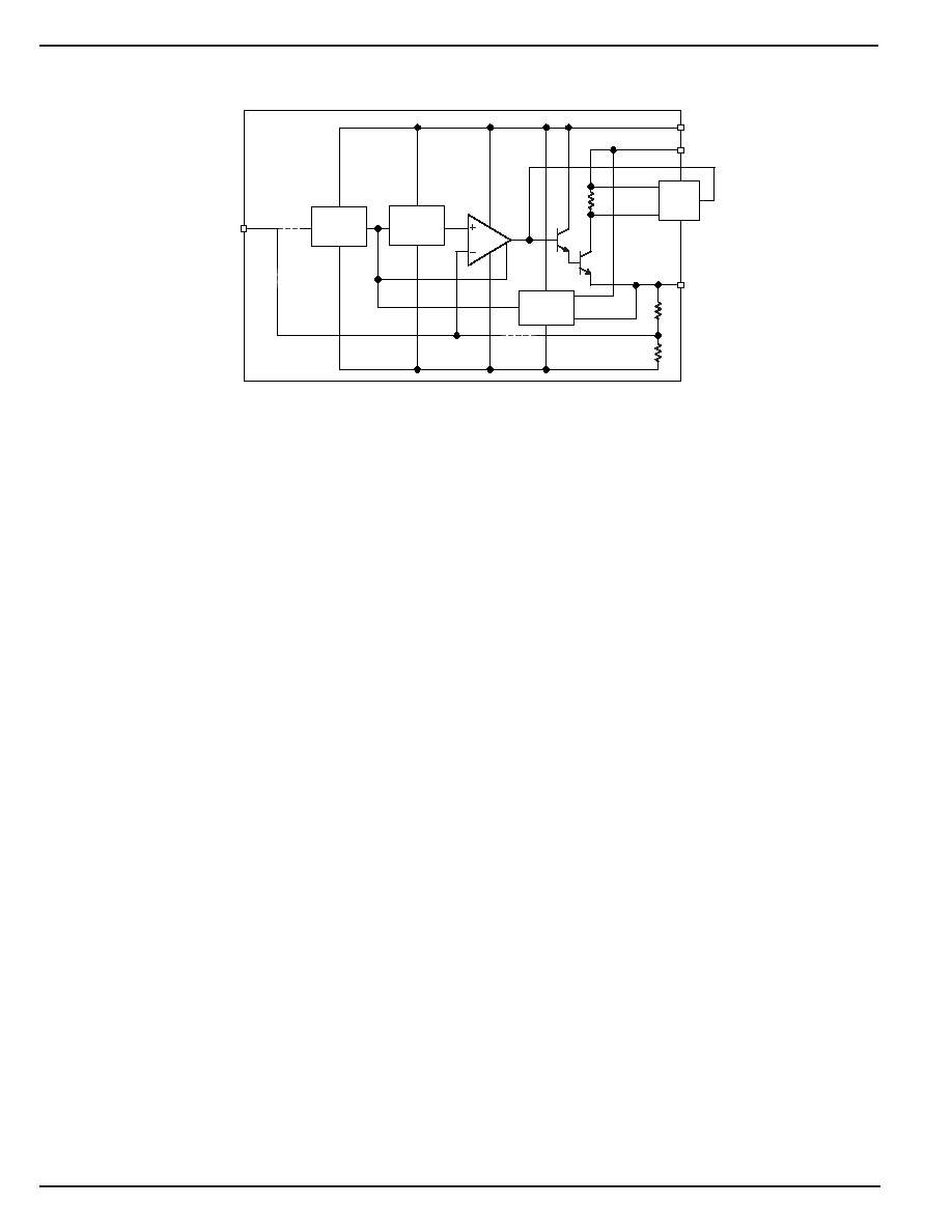
Functional Diagram
V
OUT
Enable
Bandgap
V
BIAS
V
IN
Ilimit
V
IN
Open
Circuit
R1
R2
Fixed
Adj.
Fixed
V
EN
/
ADJ
October 2003
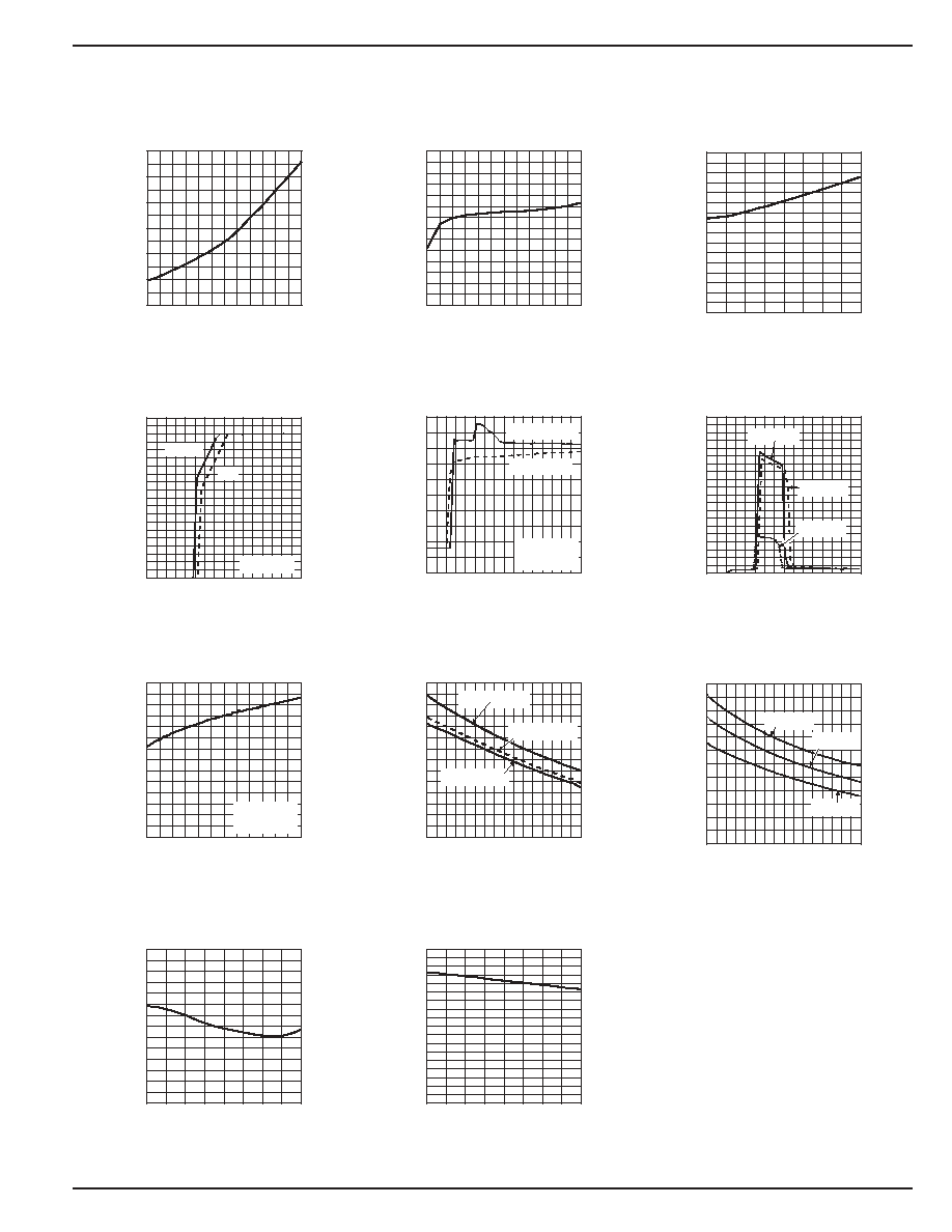
5
MIC49300
MIC49300
Micrel
0
50
100
150
200
250
300
0
0.5
1
1.5
2
2.5
3
V
IN
DROPOUT (mV)
OUTPUT CURRENT (A)
V
IN
Dropout
vs. Output Current
1
1.1
1.2
1.3
1.4
1.5
1.6
1.7
0
0.5
1.0
1.5
2.0
2.5
3.0
V
BIAS
DROPOUT (V)
OUTPUT CURRENT (A)
V
BIAS
Dropout
vs. Output Current
0
50
100
150
200
250
300
350
400
-40 -20 0
20 40 60 80 100 120
V
IN
DROPOUT (mV)
TEMPERATURE (
∞
C)
Dropout vs.
Temperature (Input Supply)
0
0.2
0.4
0.6
0.8
1.0
1.2
1.4
1.6
1.8
2.0
0 0.5 1.0 1.5 2.0 2.5 3.0 3.5 4.0
OUTPUT VOLTAGE (V)
SUPPLY VOLTAGE (V)
Dropout Characteristics
V
BIAS
= 5V
100mA
3A
0
5
10
15
20
25
0 0.5 1 1.5 2 2.5 3 3.5 4
BIAS CURRENT (mA)
INPUT SUPPLY (V)
Bias Current
vs. Input Supply
V
OUT
= 1.8V
V
BIAS
= 5V
I
OUT
= 0mA
I
OUT
= 100mA
0
100
200
300
400
500
600
700
800
900
1000
0 0.5 1.0 1.5 2.0 2.5 3.0 3.5 4.0
BIAS CURRENT (mA)
SUPPLY VOLTAGE (V)
Bias Current
vs. Supply Voltage
I
OUT
= 1A
I
OUT
= 3A
I
OUT
= 2A
0
5
10
15
20
25
30
35
0
0.5
1.0
1.5
2.0
2.5
3.0
BIAS CURRENT (mA)
OUTPUT CURRENT (A)
Bias Current
vs. Output Current
V
BIAS
= 5V
V
IN
= 2.5V
0
5
10
15
20
25
30
35
-40 -20 0
20 40 60 80 100 120
BIAS CURRENT (mA)
TEMPERATURE (
∞
C)
Bias Current
vs. Temperature
I
OUT
= 100mA
I
OUT
= 100
µ
A
I
OUT
= 500mA
0
10
20
30
40
50
60
-40 -20 0
20 40 60 80 100 120
BIAS CURRENT (mA)
TEMPERATURE (
∞
C)
Bias Current
vs. Temperature
I
OUT
= 1A
I
OUT
= 3A
I
OUT
= 2A
1.764
1.774
1.784
1.794
1.804
1.814
1.824
1.834
-40 -20 0
20 40 60 80 100 120
OUTPUT VOLTAGE (V)
TEMPERATURE (
∞
C)
Output Voltage
vs. Temperature
0
1
2
3
4
5
6
7
8
9
-40 -20 0
20 40 60 80 100 120
SHORT CIRCUIT CURRENT (A)
TEMPERATURE(
∞
C)
Short Circuit
vs. Temperature
Typical Characteristics

MIC49300
Micrel
MIC49300
6
October 2003
Applications Information
The MIC49300 is an ultra-high performance, low dropout
linear regulator designed for high current applications requir-
ing fast transient response. The MIC49300 utilizes two input
supplies, significantly reducing dropout voltage, perfect for
low-voltage, DC-to-DC conversion. The MIC49300 requires
a minimum of external components and obtains a bandwidth
of up to 10MHz. As a
µ
Cap regulator, the output is tolerant of
virtually any type of capacitor including ceramic and tanta-
lum.
The MIC49300 regulator is fully protected from damage due
to fault conditions, offering linear current limiting and thermal
shutdown.
Bias Supply Voltage
V
BIAS
, requiring relatively light current, provides power to the
control portion of the MIC49300. V
BIAS
requires approxi-
mately 33mA for a 1.5A load current. Dropout conditions
require higher currents. Most of the biasing current is used to
supply the base current to the pass transistor. This allows the
pass element to be driven into saturation, reducing the
dropout to 300mV at a 1.5A load current. Bypassing on the
bias pin is recommended to improve performance of the
regulator during line and load transients. Small ceramic
capacitors from V
BIAS
to ground help reduce high frequency
noise from being injected into the control circuitry from the
bias rail and are good design practice. Good bypass tech-
niques typically include one larger capacitor such as a 1
µ
F
ceramic and smaller valued capacitors such as 0.01
µ
F or
0.001
µ
F in parallel with that larger capacitor to decouple the
bias supply. The V
BIAS
input voltage must be 1.6V above the
output voltage with a minimum V
BIAS
input voltage of 3V.
Input Supply Voltage
V
IN
provides the high current to the collector of the pass
transistor. The minimum input voltage is 1.4V, allowing
conversion from low voltage supplies.
Output Capacitor
The MIC49300 requires a minimum of output capacitance to
maintain stability. However, proper capacitor selection is
important to ensure desired transient response. The MIC49300
is specifically designed to be stable with virtually any capaci-
tance value and ESR. A 1
µ
F ceramic chip capacitor should
satisfy most applications. Output capacitance can be in-
creased without bound. See typical characteristics for ex-
amples of load transient response.
X7R dielectric ceramic capacitors are recommended be-
cause of their temperature performance. X7R-type capaci-
tors change capacitance by 15% over their operating tem-
perature range and are the most stable type of ceramic
capacitors. Z5U and Y5V dielectric capacitors change value
by as much as 50% and 60%, respectively, over their oper-
ating temperature ranges. To use a ceramic chip capacitor
with Y5V dielectric, the value must be much higher than an
X7R ceramic or a tantalum capacitor to ensure the same
capacitance value over the operating temperature range.
Tantalum capacitors have a very stable dielectric (10% over
their operating temperature range) and can also be used with
this device.
Input Capacitor
An input capacitor of 1
µ
F or greater is recommended when
the device is more than 4 inches away from the bulk supply
capacitance, or when the supply is a battery. Small,
surfacemount, ceramic chip capacitors can be used for the
bypassing. The capacitor should be placed within 1" of the
device for optimal performance. Larger values will help to
improve ripple rejection by bypassing the input to the regula-
tor, further improving the integrity of the output voltage.
Thermal Design
Linear regulators are simple to use. The most complicated
design parameters to consider are thermal characteristics.
Thermal design requires the following application-specific
parameters:
∑ Maximum ambient temperature (T
A
)
∑ Output Current (I
OUT
)
∑ Output Voltage (V
OUT
)
∑ Input Voltage (V
IN
)
∑ Ground Current (I
GND
)
First, calculate the power dissipation of the regulator from
these numbers and the device parameters from this datasheet.
P
D
= V
IN
◊
I
IN
+ V
BIAS
◊
I
BIAS
≠ V
OUT
◊
I
OUT
The input current will be less than the output current at high
output currents as the load increases. The bias current is a
sum of base drive and ground current. Ground current is
constant over load current. Then the heat sink thermal
resistance is determined with this formula:
SA
J(MAX)
A
D
JC
CS
T
T
P
=
+
(
)
≠
≠
The heat sink may be significantly reduced in applications
where the maximum input voltage is known and large com-
pared with the dropout voltage. Use a series input resistor to
drop excessive voltage and distribute the heat between this
resistor and the regulator. The low dropout properties of the
MIC49300 allow significant reductions in regulator power
dissipation and the associated heat sink without compromis-
ing performance. When this technique is employed, a capaci-
tor of at least 1
µ
F is needed directly between the input and
regulator ground. Refer to Application Note 9 for further
details and examples on thermal design and heat sink speci-
fication.
Minimum Load Current
The MIC49300, unlike most other high current regulators,
does not require a minimum load to maintain output voltage
regulation.
Power Sequencing
There is no power sequencing requirement for V
IN
and V
BIAS
,
giving more flexibility to the user.

October 2003
7
MIC49300
MIC49300
Micrel
Adjustable Regulator Design
The MIC49300 adjustable version allows programming the
output voltage anywhere between 0.9Vand 5V. Two resistors
are used. The resistor value between V
OUT
and the adjust pin
should not exceed 1k
. Larger values can cause instability.
The resistor values are calculated by:
R1 R2
V
OUT
=
◊
0 9
1
.
≠
Where V
OUT
is the desired output voltage.
Enable
The fixed output voltage versions of the MIC49300 feature an
active high enable input (EN) that allows on-off control of the
regulator. Current drain reduces to "zero" when the device is
sn}t
wn, with only microamperes of leakage current. The
EN input has TTL/CMOS compatible thresholds for simple
logic interfacing. EN may be directly tied to V
IN
and pulled up
to the maximum supply voltage
MIC49300
Micrel
MIC49300
8
October 2003
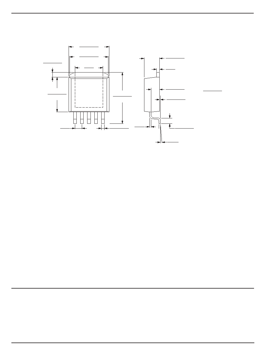
Package Information
0.370
±
0.005
9.395
±
0.125
0.355
±
0.005
9.015
±
0.125
0.315
±
0.005
8.000
±
0.130
0.415
±
0.005
10.54
±
0.130
0.028
±
0.003
0.710
±
0.080
0.075
±
0.005
1.905
±
0.125
0.040
±
0.005
1.015
±
0.125
0.003
±
0.002
0.080
±
0.050
0.036
±
0.005
0.915
±
0.125
INCHES
MILLIMETER
0
∞
min
6
∞
max
0.010
0.250
0.010
0.250
0.067
1.700
0.040
±
0.010
1.015
±
0.255
0.256
6.50
5-Lead S-Pak (R)
MICREL, INC.
1849 FORTUNE DRIVE
SAN JOSE, CA 95131
USA
TEL
+ 1 (408) 944-0800
FAX
+ 1 (408) 944-0970
WEB
http://www.micrel.com
The information furnished by Micrel in this datasheet is believed to be accurate and reliable. However, no responsibility is assumed by Micrel for its use.
Micrel reserves the right to change circuitry and specifications at any time without notification to the customer.
Micrel Products are not designed or authorized for use as components in life support appliances, devices or systems where malfunction of a product can
reasonably be expected to result in personal injury. Life support devices or systems are devices or systems that (a) are intended for surgical implant into
the body or (b) support or sustain life, and whose failure to perform can be reasonably expected to result in a significant injury to the user. A Purchaser's
use or sale of Micrel Products for use in life support appliances, devices or systems is at Purchaser's own risk and Purchaser agrees to fully indemnify
Micrel for any damages resulting from such use or sale.
© 2003 Micrel, Incorporated.