 | –≠–ª–µ–∫—Ç—Ä–æ–Ω–Ω—ã–π –∫–æ–º–ø–æ–Ω–µ–Ω—Ç: MIC5031BM | –°–∫–∞—á–∞—Ç—å:  PDF PDF  ZIP ZIP |
August 1999
1
MIC5031
MIC5031
Micrel
MIC5031
High-Speed High-Side MOSFET Driver
Not Recommended for New Designs
General Description
The MIC5031 MOSFET driver is designed to switch an
N-channel enhancement-type MOSFET from a TTL control
signal in a high-side switch application. The MIC5031 pro-
vides overcurrent protection, can accommodate loads with
high-inrush current, and is designed to survive automotive
power disturbances. This driver is suitable for up to 30kHz
PWM operation with 0% to 100% duty cycle.
The MIC5031 is powered by the +4.5V to +30V load voltage.
An external bootstrap capacitor and internal charge pump
drive the gate output higher than the supply voltage. The
bootstrap capacitor provides speed, while the charge pump
can sustain the high gate output voltage continuously.
The MIC5031 features a resistor programmable overcurrent
shutdown (circuit breaker) function that monitors the voltage
drop across the external MOSFET. A capacitor program-
mable shutdown delay allows a high-inrush current load to be
energized without causing undesired shutdown. An open-
load detection feature is included and can be used by adding
an external high-value resistor.
The MIC5031 is protected against automotive load dump and
reverse battery conditions. The driver is also protected from
excessive power dissipation by an internal overtemperature
shutdown circuit.
An open-collector fault flag output indicates overcurrent,
overtemperature, or open-load fault conditions.
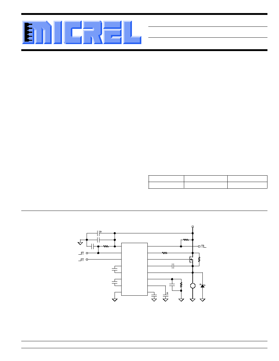
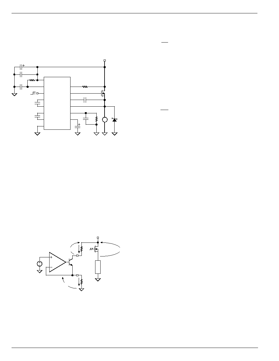
Typical Application
On
Off
FLG
RV
G
VDD
EN
CTL
100k
* Sets Overcurrent Trip to MOSFET V
DS
102mV
Optional Resistor for Open-Load Detection
Optional Capacitor for Overcurrent Delay
ß
Optional Resistor and Capacitor for Power-up Sequence
+4.5V to +30V
MIC5031
CB
CP1+
S
CP1≠
RI
CP2+
CS
CP2≠
DLY
GND
15µF
50pF
12k*
0.1µF
1k*
Normal
Fault
51k
0.01µF
0.01µF
Enable
Disable
7
4
3
10
8
11
9
5
2
6
15
13
12
16
14
1
IRF540
0.1µF
M
2N5822
100µF
100nF
10k
ß
0.01µF
ß
High-Side Power Switch and Circuit Breaker
Features
∑ +4.5V to +30V operation
∑ Fast gate drive
(rise time = 70ns, fall time = 50ns,
with 1000pF load and 5V supply)
∑ Overcurrent detection across MOSFET
∑ Overcurrent shutdown delay
∑ Charge pump for high-side dc applications
∑ TTL compatible input
∑ Overtemperature shutdown
∑ Automotive load dump protection
∑ Reverse battery protection
∑ Open-collector fault flag
∑ Near zero-current disable state
Applications
∑ Automotive power switch
∑ Automotive PWM control
∑ Circuit breaker
∑ PWM circuits
Ordering Information
Part Number
Temperature Range
Package
MIC5031BM
≠40
∞
C to +85
∞
C
16-lead SOIC
Micrel, Inc. ∑ 1849 Fortune Drive ∑ San Jose, CA 95131 ∑ USA ∑ tel + 1 (408) 944-0800 ∑ fax + 1 (408) 944-0970 ∑ http://www.micrel.com
MIC5031
Micrel
MIC5031
2
August 1999
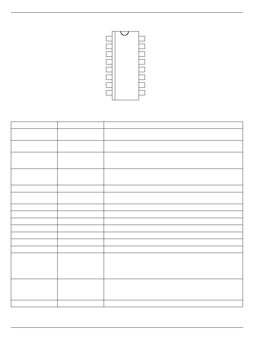
Pin Configuration
8
CP1≠
2
DLY
RV
14
3
CTL
S
13
4
EN
CB
12
5
GND
CP2+
11
6
CS
CP1+
10
7
VDD
CP2≠
9
1
FLG
RI
15
G
16
16-lead SOIC (M)
Pin Description
Pin Number
Pin Name
Pin Function
1
FLG
Fault Flag: (Output): Open-collector output sinks current upon overcurrent,
open-load, or overtemperature detection. 10mA maximum load.
2
DLY
Overcurrent Delay Time Capacitor: Optional. Capacitor to ground delays
activation of overcurrent shutdown.
3
CTL
Control (Input): TTL compatible on/off control input. Logic high drives the
gate output above the supply voltage. Logic low forces the gate output near
ground. Logic low also resets the overcurrent fault latch.
4
EN
Enable (Input): CMOS compatible input. Logic high enables the charge
pump. Logic low disables the charge pump and draws near zero supply
current.
5
GND
Ground: Power return.
6
CS
Internal Supply Storage Capacitor: 10
µ
F external capacitor to GND.
Provides additional current to internal circuitry during switching transitions.
7
VDD
Supply (Input): +4.5V to +30V supply.
8
CP1≠
Charge Pump Capacitor #1: Refer to CP1+.
9
CP2≠
Charge Pump Capacitor #2: Refer to CP2+.
10
CP1+
Charge Pump Capacitor #1: External 0.01
µ
F voltage tripler capacitor.
11
CP2+
Charge Pump Capacitor #2: External 0.01
µ
F voltage tripler capacitor.
12
CB
Bootstrap Capacitor: 0.1
µ
F capacitor to source for fastest rise time.
13
S
Source: Source connection to external MOSFET.
14
RV
Reference Voltage Resistor: Resistor to VDD provides a reference voltage
drop. A voltage drop across the external MOSFET that is greater than the
voltage drop across the reference resistor indicates an overcurrent condition.
(
Refer to applications section) Zero temperature coefficient resistor
recommended.
15
RI
Reference Current Resistor: Resistor to GND sets constant current value
through RV resistor (
Refer to applications section) and matches tempera-
ture compensation of RV resistor. Zero temperature coefficient resistor
recommended.
16
G
Gate (Output) : Gate connection to external MOSFET.

August 1999
3
MIC5031
MIC5031
Micrel
Electrical Characteristics
V
DD
= 12V; C
B
= 0.1
µ
F, CP1 = CP2 = 0.01
µ
F; T
A
= 25
∞
C; unless noted
Symbol
Parameter
Condition
Min
Typ
Max
Units
I
DD
Supply current
V
EN
= 0V, V
CTL
= 0V
0.3
3
µ
A
V
EN
= 12V, V
CTL
= 0V
1.0
mA
V
EN
= 12V, V
CTL
= 5V
0.72
mA
I
DDR
Reverse voltage leakage current
V
DD
= ≠12V
≠0.2
≠5
µ
A
V
CTL
Control input voltage threshold
1.55
V
V
CTLH
Control input voltage hysteresis
0.2
0.5
1.0
V
I
CTL
Control input current
0.1
1
µ
A
V
EN
Enable input voltage threshold
6
V
I
EN
Enable input current
0.1
1
µ
A
V
IOS
Overcurrent comparator offset
±
5
mV
I
RV
Current limit reference current
R
RI
= 12.0k
97
100
103
µ
A
t
SHDL
Overcurrent shut down delay
C
DLY
= 50pF
16
µ
s
V
G
Gate drive voltage
V
EN
= 12V, V
CTL
= 5V
25
V
t
DLR
Gate turn-on delay
V
EN
= 12V, C
L
= 1000p
420
ns
t
R
Gate rise time
C
L
= 1000pF
90
ns
t
DLF
Gate turnoff delay
C
L
= 1000pF
300
ns
t
F
Gate fall time
C
L
= 1000pF
50
ns
V
OLTH
Open-load threshold voltage
V
EN
= 12V, V
CTL
= 0V
6.3
V
T
OT
Overtemperature shut down
V
EN
= 12V, V
CTL
= 5V
140
∞
C
T
OTH
Overtemp. shut down hysteresis
V
EN
= 12V, V
CTL
= 5V
10
∞
C
f
CP
Charge pump frequency
V
DD
= 5V, Note 1
190
kHz
V
FLG
Flag active voltage
open load error, I
FLG
= 2mA (sink)
0.2
V
General Note: Devices are ESD protected; however, handling precautions are recommended.
Note 1:
Oscillator burst mode at V
DD
5.2V.
Absolute Maximum Ratings
Supply Voltage (V
DD
) .................................................. +36V
Enable Input Voltage (V
EN
) ......................................... +36V
Control Input Voltage (V
CTL
)
V
DD
15V .................................................................. V
DD
V
DD
> 15V ............................................................... +15V
Flag Output Voltage (V
FLG
) ......................................... +36V
Reference Voltage Input (V
RV
) .................................... +36V
Junction Temperature (T
J
) ........................................ 150
∞
C
Operating Ratings
Supply Voltage (V
DD
) ................................... +4.5V to +30V
Ambient Temperature Range (T
A
)
A-temperature range ............................ ≠55
∞
C to +125
∞
C
B-temperature range .............................. ≠40
∞
C to +85
∞
C
Package Thermal Resistance (
JA
)
SOIC ................................................................. 115
∞
C/W
MIC5031
Micrel
MIC5031
4
August 1999
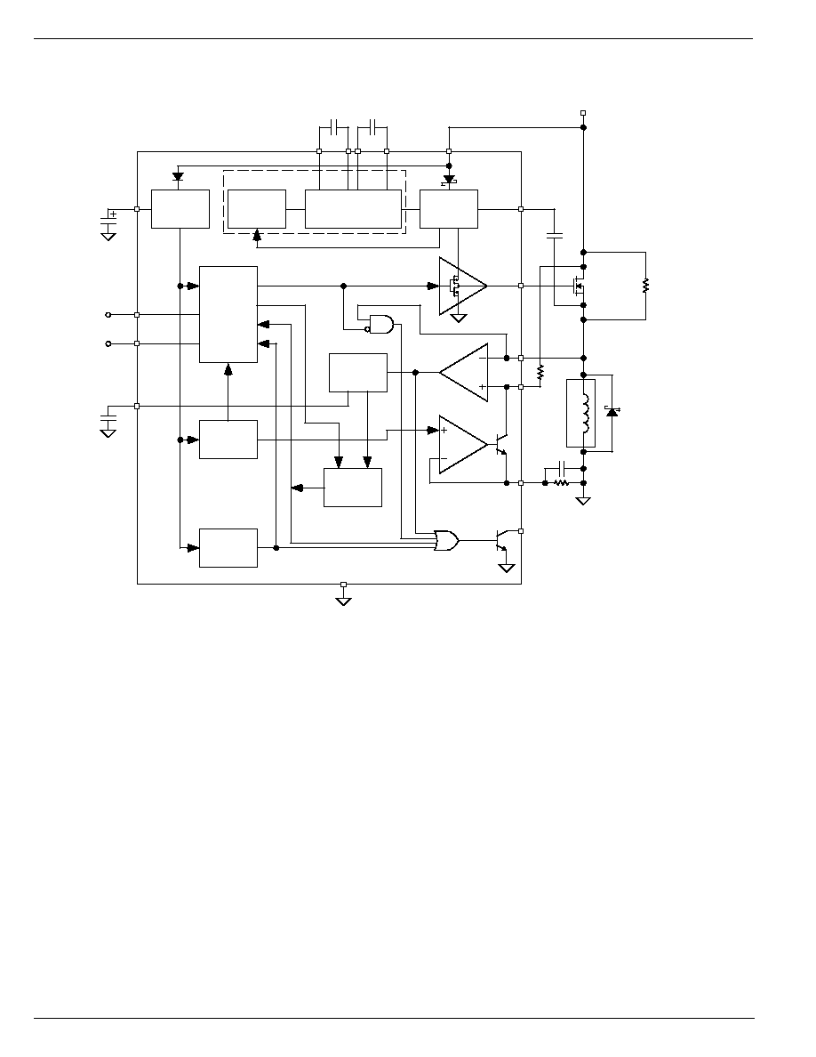
Block Diagram
RV
RI
External
N-Channel
MOSFET
R1
R2
CP1+
CP2≠
CP1+
CP1≠
Oscillator
Voltage
Tripler
Gate Drive
Regulator
Bias
Regulator
1.23V
Bandgap
Reference
Overtemp.
Detect
Logic
Current Limit
Delay
Lockout
Latch
Open-Load Detect
Reset
Voltage
Comp.
Ref.
Current
Amp.
CTL
(TTL)
EN
(CMOS)
DLY
CS
Open-Load
Detect
Resistor
(Optional)
Gate
Driver
Osc. Disable
FLAG
S
G
CB
VDD
V
SUPPLY
MIC5031
GND
Inductive Load
C3
C1
C2
C4
Charge Pump
Overcurrent
Delay
Capacitor
(Optional)
MIC5031 with External Components
August 1999
5
MIC5031
MIC5031
Micrel
Functional Description
Refer to "Functional Diagram."
The MIC5031 is a noninverting device. Applying a CMOS
logic high signal to EN (enable input) activates the driver's
internal circuitry. Applying a TTL logic high signal to CTL
(control input) produces gate drive output. The G (gate)
output is used to turn on an external N-channel MOSFET.
Control
CTL (control) is a TTL compatible input. The threshold is
approximately 1.4V, independent of the supply voltage.
The falling edge of a signal applied to CTL also resets the
overcurrent lockout latch.
Enable
EN (enable) is a CMOS compatible input. EN enables or
disables all internal circuitry. The enable threshold is approxi-
mately half the supply voltage. The MIC5031 supply current
is near zero when the driver is disabled (low). See "Applica-
tions Information: Power-Up Sequence."
Charge Pump
The charge pump produces a voltage that is higher than the
supply voltage. This higher voltage is required to drive the
external N-channel MOSFET in high-side switch circuits.
The charge pump consists of an oscillator and a voltage
tripler. When the driver is enabled, the charge pump is
switched on and off to regulate its output voltage.
External capacitors C1 and C2 are required. The charge
pump will not operate without these capacitors.
Bootstrap Capacitor
The external bootstrap capacitor is necessary to achieve the
fastest gate rise times. The bootstrap capacitor (C3) supplies
additional current at a higher voltage to the gate drive
regulator as the MOSFET is switched on.
When the MOSFET is off, the gate drive regulator voltage is
applied to the boost capacitor . As the MOSFET turns on, the
MOSFET source-to-ground voltage increases. The increas-
ing source voltage is added to the voltage across the capaci-
tor for a voltage doubling effect.
Gate Drive Regulator
The gate drive regulator manages the voltage from the
bootstrap capacitor, the supply, and the charge pump.
The gate drive regulator charges the bootstrap capacitor
when the MOSFET is off and limits the voltage from the
bootstrap capacitor as the MOSFET is switched on. It also
performs skip-mode control by switching the charge pump on
and off to regulate the gate drive output voltage.
Gate Output
When the MIC5031 is enabled and CTL is high, the gate
driver steers regulated voltage to G (gate output). When CTL
is low, the gate driver grounds G. This respectively charges
or discharges the external MOSFET's gate, .
Current Sense
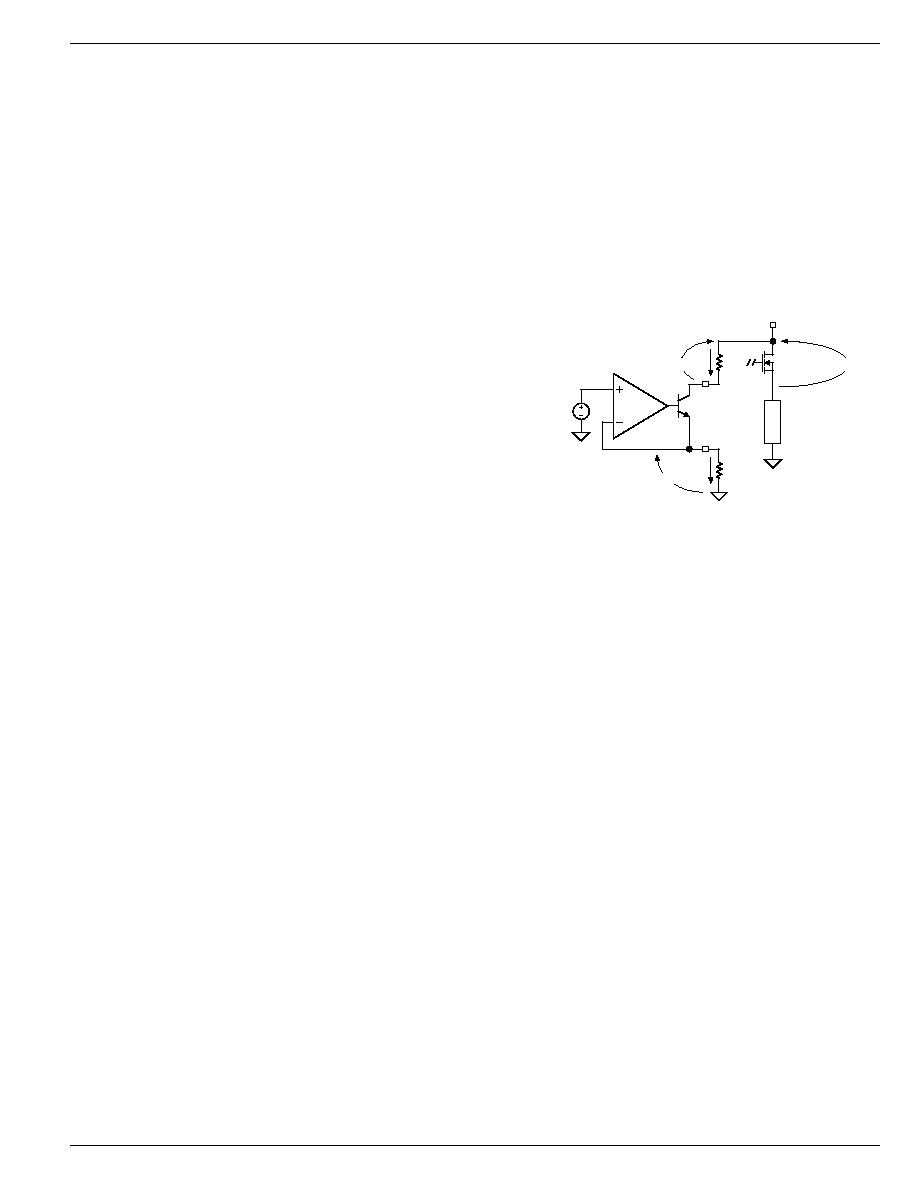
Refer to the "Voltage Reference (Simplified)" diagram.
The MIC5031 detects an overcurrent condition by comparing
the voltage drop across the external MOSFET to a reference
voltage drop created across R1. If V
DS
exceeds V
R1
, a
comparator (not shown) shuts off the external MOSFET by
way of the current limit delay, lockout latch, and logic.
The bandgap reference, op amp and NPN create a constant
voltage (1.23V) across R2. This results in a constant current,
I
R2
, through R2. Ignoring a small amount of base current, the
same current (I
R2
) flows through R1. R1 is selected to
achieve the desired reference voltage drop, V
R1
. Refer to the
applications section for formulas.
Supply
1.23V
Bandgap
Reference
RV
RI
External
N-Channel
MOSFET
Load
V
DS
V
R1
I
R2
R1
R2
1.23V
I
R2
Voltage Reference (Simplified)
An overcurrent condition also activates the fault flag output
when the lockout latch is activated.
Overcurrent-Shutdown Delay
The overcurrent-shutdown delay circuit permits a delay be-
tween overcurrent detection and latch activation for high-
inrush current loads.
The delay can be increased by adding capacitance from DLY
to GND.
Open-Load Detect
The open load detect resistor is an external high-value pull-
up resistor that causes the source voltage of the external
MOSFET to increase when the load is missing.
The MIC5031 monitors the S-pin voltage only when the gate
driver is off. If the voltage on the S-pin rises above the open-
load detect threshold, the fault flag is activated.
Overtemperature Detect
The overtemperature detect circuit switches the logic to turn
the output off at approximately 140
∞
C. An overtemperature
shutdown condition is restored to normal automatically When
the device cools to about 130
∞
C (10
∞
C hysteresis).
An overtemperature condition also activates the fault flag
output.
Fault Flag
FLT (fault flag) is an open-collector NPN transistor. Fault is
active (pulls collector near ground) upon overcurrent, open-
load, or overtemperature.
MIC5031
Micrel
MIC5031
6
August 1999
Applications Information
Power-Up Sequence
The supply voltage (V
DD
) must be applied to VDD before EN
is asserted. If EN is not required for the application, an RC
network must be used to delay the voltage rise applied to EN
with respect to VDD. See Figure 1.
On
Off
FLG
RV
G
VDD
EN
CTL
+4.5V to +30V
MIC5031
CB
CP1+
S
CP1≠
RI
CP2+
CS
CP2≠
DLY
GND
15µF
12k*
0.1µF
0.01µF
0.01µF
7
4
3
10
8
11
9
5
2
6
15
13
12
16
14
1
IRF540
0.1µF
M
2N5822
100µF
100nF
0.01µF
10k
Figure 1. Enable Application
Refer to "Typical Application" for controlling EN from open-
collector or open-drain logic. The 10k resistor and 0.01
µ
F
capacitor connected to VDD, GND, and EN keep EN low
during power up before the open-collector or open-drain logic
becomes active.
The 10k resistor and 0.01
µ
F capacitor can be omitted if EN
is held low by the external logic until VDD is powered.
Overcurrent Detection
Using the MOSFET manufacturer's data and the maximum
allowable load current, determine the maximum drain-to-
source voltage drop, V
DS
, that will occur across the external
MOSFET in normal operation. This will also be the reference
voltage and the overcurrent trip voltage, V
R1
.
V
R1
= maximum R
DS(on)
◊
maximum load current
Supply
1.23V
Bandgap
Reference
RV
RI
External
N-Channel
MOSFET
Load
V
DS
V
R1
I
R2
R1
R2
1.23V
I
R2
Figure 2. Resistor Calculations
Reference Current Resistor
Resistor R2 sets the reference current. For most applica-
tions, a reference current of 100
µ
A is suggested.
R2
R1
I
R2
=
where:
R2 = reference current resistor (
)
I
R2
= reference current (A) [R2 = 12k
for
approximately 100
µ
A]
Reference Voltage Resistor
The reference voltage resistor value is calculated from the
reference current and the reference voltage (overcurrent
drop voltage).
R1
V
I
R1
R2
=
where:
R1 = reference voltage resistor (
)
V
R1
= reference voltage (V) [see above]
I
R2
= reference current (A) [see above]
Overcurrent Delay Capacitor
For lamp switching applications, the delay capacitor (C
DLY
)
may be as high as several microfarads. Lamps often have an
inrush current of 10
◊
their steady-state operating current. In
PWM applications, pay attention to the input frequency vs.
the overcurrent delay. They can conflict with each other if not
properly planned.
August 1999
7
MIC5031
MIC5031
Micrel
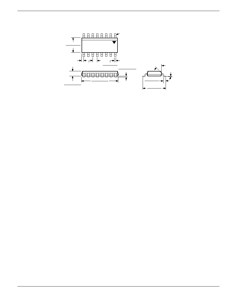
Package Information
45
∞
0
∞
≠8
∞
0.244 (6.20)
0.228 (5.79)
0.394 (10.00)
0.386 (9.80)
SEATING
PLANE
0.020 (0.51)
REF
0.020 (0.51)
0.013 (0.33)
0.157 (3.99)
0.150 (3.81)
0.050 (1.27)
0.016 (0.40)
0.0648 (1.646)
0.0434 (1.102)
0.050 (1.27)
BSC
PIN 1
DIMENSIONS:
INCHES (MM)
0.0098 (0.249)
0.0040 (0.102)
16-Lead SOIC (M)

MIC5031
Micrel
MIC5031
8
August 1999
MICREL INC.
1849 FORTUNE DRIVE
SAN JOSE, CA 95131
USA
TEL
+ 1 (408) 944-0800
FAX
+ 1 (408) 944-0970
WEB
http://www.micrel.com
This information is believed to be accurate and reliable, however no responsibility is assumed by Micrel for its use nor for any infringement of patents or
other rights of third parties resulting from its use. No license is granted by implication or otherwise under any patent or patent right of Micrel Inc.
© 1999 Micrel Incorporated