8-4
August 1998
MIC50395/50396/50397
Micrel
General Description
The MIC50395 is an ion-implanted, P-channel MOS six-
decade synchronous up/down-counter/display driver with
compare-register and storage-latches. The counter as well
as the register can be loaded digit-by-digit with BCD data.
The counter has an asynchronous-clear function.
Scanning is controlled by the scan oscillator input which is
self-oscillating or can be driven by an external signal. The
six-decade register is constantly compared to the state of
the six-decade counter and when both the register and the
counter have the same content, an EQUAL signal is gener-
ated. The contents of the counter can be transferred into the
6-digit latch which is then multiplexed from MSD to LSD in
BCD and 7-segment format to the output. The seven-
segment decoder incorporates a leading-zero blanking
circuit which can be disabled by an external signal. This
device is intended to interface directly with the standard
CMOS logic families.
The MIC50396 and MIC50397 operate identically to the
MIC50395 except that two digits in each were reprogrammed
to provide divide by six circuitry instead of divide by ten. The
MIC50396 is well suited for industrial timer applications while
the MIC50397 is best suited for stop watch or real time
computer clock applications.
Features
∑
Single power supply
∑
Schmitt-Trigger on the count-input
∑
Drives common anode or cathode displays (CA with buffer)
∑
Six decades of synchronous up/down counting
∑
Look-ahead carry or borrow
∑
Loadable counter
∑
Loadable compare-register with comparator output
∑
Multiplexed BCD and seven-segment outputs
∑
Internal scan oscillator
∑
Direct LED segment drive
∑
Interfaces directly with CMOS logic
∑
Leading zero blanking
∑
MIC50396 programmed to count time:
≠ 99 hrs. 59 min. 59 sec.
∑
MIC50397 programmed to count time:
≠ 59 hrs. 59 min. 99/100 min.
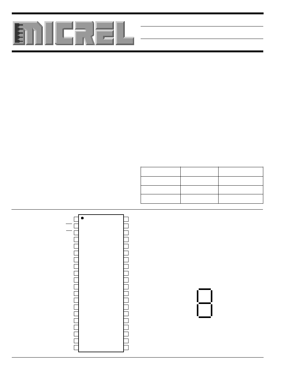
MIC50395/50396/50397
Six Decade Counter / Display Decoder
Pin Connection
Ordering Information
Part Number
Temp. Range
Package
MIC50395CN
0
∞
C to 70
∞
C
40-pin Plastic DIP
MIC50396CN
0
∞
C to 70
∞
C
40-pin Plastic DIP
MIC50397CN
0
∞
C to 70
∞
C
40-pin Plastic DIP
1
40
2
39
3
38
4
37
5
36
6
35
7
34
8
33
9
32
10
31
11
30
12
29
13
28
14
27
15
26
16
25
17
24
18
23
19
22
20
21
UP/DOWN
ZERO
CARRY
COUNT INHIBIT
COUNT
R A
R B
R C
R D
REGISTER
BCD
IN
LOAD COUNTER
LOAD REGISTER
D 6
D 5
D 4
D 3
MSD
DIGIT
D 2
D 1
STROBES
LSD
EQUAL
SCAN
V DD
MIC50395CN
MIC50396CN
MIC50397CN
SET
LZB
a
b
c
d
e
f
g
A
B
C
D
C D
C C
C B
C A
CLEAR
STORE
SEGMENTS
BCD
OUT
COUNTER
BCD
IN
V SS
a
g
d
f
e
b
c
Segment Identification
Not Recommended for New Designs

August 1998
8-5
MIC50395/50396/50397
Micrel
8
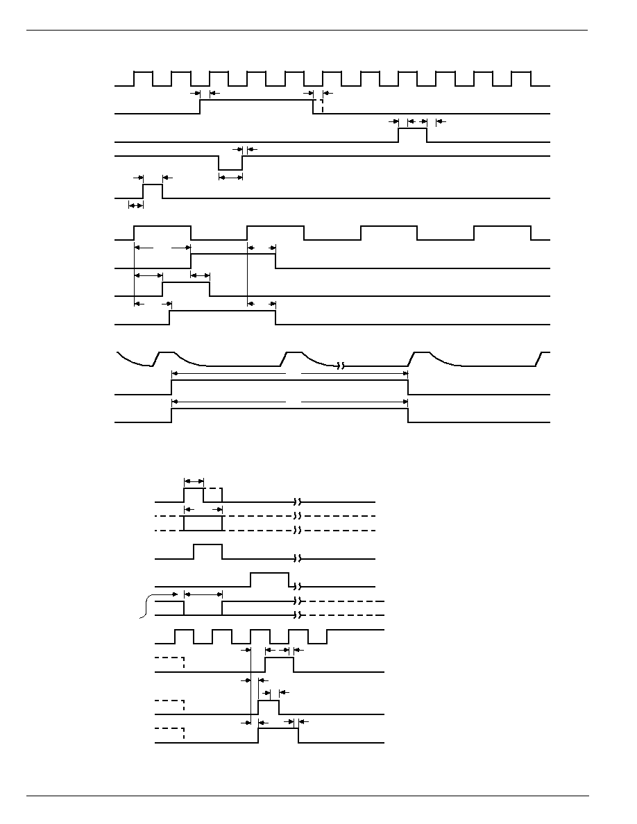
Operations:
Six Decade Counter, Latch
The six decade counter is synchronously incremented or
decremented on the positive edge of the count input signal.
A Schmitt trigger on this input provides hysteresis for protec-
tion against both a noisy environment and double triggering
due to a slow rising edge at the count input.
The count inhibit can be changed in coincidence with
the positive transition of the count input; the count input is
inhibited when the count inhibit is high.
The counter will increment when up/down input is high (V
SS
)
and will decrement when up/down input is low. The up/down
input can be changed 0.75
µ
s prior to the positive transition
of the count input.
The clear input is asynchronous and will reset all decades to
zero when brought high but does not affect the six digit latch
or the scan counter.
As long as store input is low, data is continuously transferred
from the counter to the display. Data in the counter will be
latched and displayed when store input is high. Store can be
changed in coincidence with the positive transition of the
count input.
The counter is loaded digit by digit corresponding to the digit
strobe outputs. BCD thumb wheel switches with four diodes
per decade connected between the digit strobe outputs and
the BCD inputs is one method to supply BCD data for
loading the counter decades.
The load counter pulse must be at V
SS
2
µ
s prior to the
positive transition of the digit strobe of the digit to be loaded.
The load counter pulse may be removed after the positive
transition of the digit strobe since the chip internally latches
this signal. The BCD data to be loaded must be valid through
the negative transition of the digit strobe.
Inputs, Outputs
The seven segment outputs are open drain capable of
sourcing 10mA average current per segment over one digit
cycle. Segments are on when at V
SS
. The Carry, Equal,
Zero, BCD and digit strobe outputs are push pull and are on
when at V
SS
. All inputs except Counter BCD, Register BCD,
and SCAN inputs are high impedance CMOS compatible.
Three basic outputs originate from the counter: zero output,
equal output, and carry output. Each output goes high on the
positive (V
SS
) going edge of the count input under the
following conditions:
Zero output goes high for one count period when all decades
contain zero. During a load counter operation the zero
output is inhibited.
Equal output goes high for one count period when the con-
tents of the counter and compare register are equal. The
equal output is inhibited by a load counter or load register
operation, which lasts until the next interdigit blanking period
following a negative transition of Load Counter or Load
Register.
The carry output goes high with the leading edge of the
count input at the count of 000000 when counting up or at
999999* when counting down and goes low with the negative
going edge of the same count input.
A count frequency of 1 MHz can be achieved if the equal
output, zero output and carry output are not used. These
outputs do not respond at this frequency due to their output
delay illustrated on the timing diagram.
Six Decade Compare Register
The register is loaded identically to the load counter paragraph
described previously. The register may be loaded
independently of the counter, however, the clear input will
not remove the register contents. Contents of the register
are not displayed by the BCD or seven segment outputs.
BCD Seven Segment Outputs
BCD or seven segment outputs are available. Digit strobes
are decoded internally by a divide by six Johnson counter.
This counter scans from MSD to LSD. By bringing the SET
input low, this counter will be forced to the MSD decade
count. During this time the segment outputs are blanked to
protect against display burn out.
BCD outputs are valid for MSD when SET is low. Applying
V
SS
to SET allows normal scan to resume. Digit 6 output is
active (V
SS
) until the next scan clock pulse brings up digit 5
output.
The segment outputs and digit strobes are blanked during
the interdigit blanking time. Leading zero blanking affects
only the segment outputs. This option is disabled by bringing
the LZB input high. Typically the interdigit blanking time is 5
to 25
µ
s when using the internal scan oscillator.
BCD output data changes at the beginning of the interdigit
blanking time. Therefore the BCD output data is valid when
the positive transition of a digit output occurs.
Scan Oscillator
The MIC50395 has an internal scan oscillator. The frequency
of the scan oscillator is determined by an external capacitor
between V
SS
or V
DD
and scan input. The wave form present
on the scan oscillator input is triangular in the self oscillate
mode.
An external oscillator may also be used to drive the scan
input. In either case, external capacitors of 150pF each will
be required from V
SS
to Counter BCD inputs and register
BCD inputs. This will allow asynchronous loading of the
BCD inputs.
In the internal drive mode the interdigit blanking time will be
the sum of the negative dwell period of the external oscillator
and the normal self oscillate blanking time. (5
25
µ
s). Dis-
play brightness can be controlled by the duty cycle of the
external scan oscillator.
*Carry occurs at 99:59:59 for the 50396 and 59:59:99 for the 50397

August 1998
8-7
MIC50395/50396/50397
Micrel
8
Absolute Maximum Ratings
Voltage on Any Terminal Relative to V
SS
+0.3V to ≠20V
Operating Temperature Range (Ambient)
0
∞
C to +70
∞
C
Storage Temperature Range (Ambient)
≠40
∞
C to +100
∞
C
Electrical Characteristics
(V
DD
= 0V, V
SS
= +10.0V to +15.0, 0
∞
C
T
A
70
∞
C)
Static Operating Conditions
Symbol
Parameter
Min
Max
Units
Notes
V
IL
Input Low Voltage, "0"
V
DD
0.2 V
SS
V
V
IH
Input High Voltage, "1"
V
SS
≠ 1
V
SS
V
4
V
OL
Output Voltage "0" @ 30
µ
A
0.2 V
SS
V
5
V
OH
Output Voltage "1" @ 1.5 mA
0.8 V
SS
V
5
I
OH
Output Current "1"
Digit strobes
3.0
mA
6
Segment outputs
10.0
mA
7
I
SCAN
Scan Input Pullup Current @ 0 V
5.5
mA
I
SCAN
Scan Input Pulldown Current @ 15 V
2
40
µ
A
I
SET
SET Input Pullup Current @ 0V
5
60
µ
A
Note 1: With 150 pF capacitor to V
SS
from counter BCD and register BCD inputs.
Note 2: I
SS
with inputs and outputs open at 0
∞
C. 33 mA at 25
∞
C and 28 mA at 70
∞
C. This does not include segment current.
Total power per segment must be limited not to exceed power dissipation of package. (
JA
= 100
∞
C/Watt)
Note 3: All outputs loaded.
Note 4: MIN V
IH
from R
A
R
B
R
C
R
D
C
A
C
B
C
C
C
D
inputs is V
SS
≠ 2.5 V. Those inputs have internal pulldown resistors to V
DD
.
Note 5: This applied to the push pull CMOS compatible outputs. Does not include digit strobes or segment outputs.
Note 6: For V
OUT
= V
SS
≠ 2.0 Volts. Average value over one digit cycle.
Note 7: For V
OUT
= V
SS
≠ 3.0 Volts. Average value over one digit cycle.
Maximum Operating Conditions
Symbol
Parameter
Min
Max
Units
Notes
T
A
Operating Temperature
0
70
∞
C
V
SS
Supply voltage (V
DD
= 0V)
10
15
V
1
I
SS
Supply Current
35
mA
2
B
V
Break Down Voltage
(Segment only @ 10
µ
A)
V
SS
≠ 26
V
P
D
Power Dissipation
670
mW
3