
March 1999
1
MIC5156/5157/5158
MIC5156/5157/5158
Micrel
MIC5156/5157/5158
Super LDOTM Regulator Controller
Final Information
either 3.3V, 5.0V, or 12V. The MIC5158 can be configured as
a fixed 5V controller or programmed to any voltage from 1.3V
to 36V using two external resistors.
The MIC5156 is available in an 8-pin DIP or SOP. The
MIC5157 and MIC5158 are available in a 14-pin DIP or SOP
which operate from ≠40
∞
C to +85
∞
C.
Features
∑ 4.5mA typical operating current
∑ <1
µ
A typical standby current
∑ Low external parts count
∑ Optional current limit (35mV typical threshold)
∑ 1% initial output voltage tolerance in most configurations
∑ 2% output voltage tolerance over temperature
∑ Fixed output voltages of 3.3V, 5.0V (MIC5156)
∑ Fixed output voltages of 3.3V, 5.0V, 12V (MIC5157)
∑ Programmable (1.3 to 36V) with 2 resistors (MIC5156/8)
∑ Internal charge pump voltage tripler (MIC5157/8)
∑ Enable pin to activate or shutdown the regulator
∑ Internal gate-to-source protective clamp
∑ All versions available in DIP and SOP
Applications
∑ Ultrahigh current ultralow dropout voltage regulator
∑ Constant high-current source
∑ Low parts count 5.0V to 3.3V computer supply
∑ Low noise/low-dropout SMPS post regulator
∑ High-current, current-limited switch
10A 5V to 3.3V Desktop Computer Regulator
General Description
The MIC5156, MIC5157, and MIC5158 Super Low-Dropout
(LDO) Regulator Controllers are single IC solutions for high-
current low-dropout linear voltage regulation. Super LDOTM
Regulators have the advantages of an external N-channel
power MOSFET as the linear pass element.
The MIC5156/7/8 family features a dropout voltage as low as
the R
DS(ON)
of the external power MOSFET multiplied by the
output current. The output current can be as high as the
largest MOSFETs can provide.
The MIC5156/7/8 family operates from 3V to 36V. The
MIC5156 requires an external gate drive supply to provide the
higher voltage needed to drive the gate of the external
MOSFET. The MIC5157 and MIC5158 each have an internal
charge pump tripler to produce the gate drive voltage. The
tripler is capable of providing enough voltage to drive a logic-
level MOSFET to 3.3V output from a 3.5V supply and is
clamped to 17.5V above the supply voltage. The tripler
requires three external capacitors.
The regulator output is constant-current limited when the
controller detects 35mV across an optional external sense
resistor. An active-low open-collector flag indicates a low
voltage of 8% or more below nominal output. A shutdown
(low) signal to the TTL-compatible enable control reduces
controller supply current to less than 1
µ
A while forcing the
output voltage to ground.
The MIC5156-3.3 and MIC5156-5.0 controllers have inter-
nally fixed output voltages. The MIC5156 [adjustable] output
is configured using two external resistors. The MIC5157 is a
fixed output controller which is externally configured to select
1
2
3
4
14
13
12
11
5
6
7
10
9
8
MIC5157
C2+
C2
≠
V
CP
GND
FLAG
3.3V
5V
C1+
C1
≠
V
DD
G
D
S
EN
V
OUT
3.3V, 10A
V
IN
(3.61V min.)
0.1µF
1.0µF
0.1µF
R
S
R
S
= 0.035V / I
LIMIT
3m
IRLZ44 (Logic Level MOSFET)
C
L
*
47µF
* Improves transient
response to load changes
Enable
Shutdown
47µF
10A Low-Dropout Voltage Regulator
1
2
3
8
7
6
4
5
MIC5156-3.3
V
P
GND
FLAG
EN
V
DD
G
D
S
V
OUT
3.3V, 10A
V
IN
5V
0.1µF
R
S
R
S
= 0.035V / I
LIMIT
3m
SMP60N03-10L
C
L
*
47µF
* Improves transient
response to load changes
+12V
Enable
Shutdown
47µF
Typical Applications
Super LDO is a trademark of Micrel, Inc.
Micrel, Inc. ∑ 1849 Fortune Drive ∑ San Jose, CA 95131 ∑ USA ∑ tel + 1 (408) 944-0800 ∑ fax + 1 (408) 944-0970 ∑ http://www.micrel.com

MIC5156/5157/5158
Micrel
MIC5156/5157/5158
2
March 1999
Pin Configuration
Ordering Information MIC5156
Part Number
Temperature Range
Voltage
Package
MIC5156-3.3BN
≠40
∞
C to +85
∞
C
3.3V
8-pin DIP
MIC5156-5.0BN
≠40
∞
C to +85
∞
C
5.0V
8-pin DIP
MIC5156BN
≠40
∞
C to +85
∞
C
Adjustable
8-pin DIP
MIC5156-3.3BM
≠40
∞
C to +85
∞
C
3.3V
8-pin SOP
MIC5156-5.0BM
≠40
∞
C to +85
∞
C
5.0V
8-pin SOP
MIC5156BM
≠40
∞
C to +85
∞
C
Adjustable
8-pin SOP
Ordering Information MIC5157
Part Number
Temperature Range
Voltage
Package
MIC5157BN
≠40
∞
C to +85
∞
C
Selectable
14-pin DIP
MIC5157BM
≠40
∞
C to +85
∞
C
Selectable
14-pin SOP
Ordering Information MIC5158
Part Number
Temperature Range
Voltage
Package
MIC5158BN
≠40
∞
C to +85
∞
C
5.0V/Adj.
14-pin DIP
MIC5158BM
≠40
∞
C to +85
∞
C
5.0V/Adj.
14-pin SOP
1
2
3
4
EN
FLAG
S (Source)
GND
V
P
D (Drain)
V
D D
G (Gate)
8
7
6
5
MIC5156-x.x
1
2
3
4
EA
5V FB
EN
FLAG
GND
S (Source)
G (Gate)
D (Drain)
14
13
12
11
MIC5158
5
6
7
V
CP
C2≠
C2+
V
D D
C1+
C1≠
10
9
8
1
2
3
4
5V
3.3V
EN
FLAG
GND
S (Source)
G (Gate)
D (Drain)
14
13
12
11
MIC5157
5
6
7
V
CP
C2≠
C2+
V
D D
C1+
C1≠
10
9
8
1
2
3
4
EN
FLAG
GND
V
P
D (Drain)
V
D D
G (Gate)
8
7
6
5
MIC5156
EA
March 1999
3
MIC5156/5157/5158
MIC5156/5157/5158
Micrel
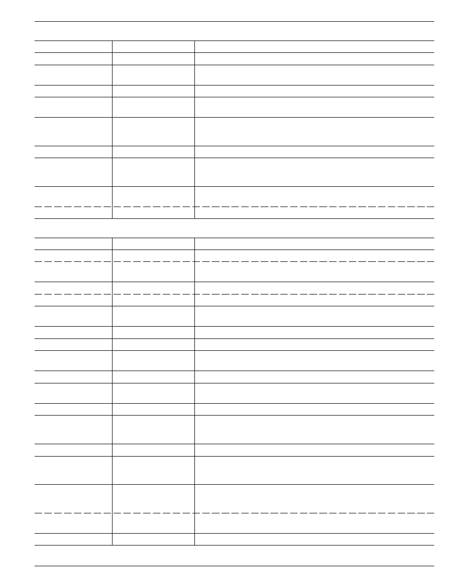
Pin Description MIC5156
Pin Number
Pin Name
Pin Function
1
EN
Enable (Input): TTL high enables regulator; TTL low shuts down regulator.
2
FLAG
Output Flag (Output): Open collector output is active (low) when V
OUT
is more
than 8% below nominal output. Circuit has 3% hysteresis.
3
GND
Circuit ground.
4
V
P
N-channel Gate Drive Supply Voltage: User supplied voltage for driving the
gate of the external MOSFET.
5
V
DD
Supply Voltage (Input): Supply voltage connection. Connect sense resistor
(R
S
) to V
DD
if current limiting used. Connect supply bypass capacitor to
ground near device.
6
G
Gate (Output): Drives the gate of the external MOSFET.
7
D
Drain and Current Limit (Input): Connect to external MOSFET drain and
external sense resistor (current limit), or connect to V
DD
and external MOSFET
drain (no current limit).
8 (3.3V, 5V)
S
Source (Input): Top of internal resistive divider chain. Connect directly to the
load for best load regulation.
8 (adjustable)
EA
Error Amplifier (Input): Connect to external resistive divider.
Pin Description MIC5157, MIC5158
Pin Number
Pin Name
Pin Function
1 (MIC5157)
5V
5V Configuration (Input): Connect to S (source) pin for 5V output.
1 (MIC5158)
EA
Error Amplifier (Input): Connect to external resistive divider to obtain adjust-
able output.
2 (MIC5157)
3.3V
3.3V Configuration (Input): Connect to S (source) pin for 3.3V output.
2 (MIC5158)
5V FB
5V Feedback (Input): Connect to EA for fixed 5V output.
3
FLAG
Output Voltage Flag (Output): Open collector is active (low) when V
OUT
is 8%
or more below its nominal value.
4
GND
Circuit ground.
5
V
CP
Voltage Tripler Output [Filter Capacitor]. Connect a 1 to 10
µ
F capacitor to ground.
6
C2≠
Charge Pump Capacitor 2: Second stage of internal voltage tripler. Connect a
0.1
µ
F capacitor from C2+ to C2≠.
7
C2+
Charge Pump Capacitor 2: See C2≠ pin 6.
8
C1+
Charge Pump Capacitor 1: First stage of internal voltage tripler. Connect a
0.1
µ
F capacitor from C1+ to C1≠.
9
C1≠
Charge Pump Capacitor 1: See C1+ pin 8.
10
V
DD
Supply Voltage (Input): Supply voltage connection. Connect sense resistor
(R
S
) to V
DD
if current limiting used. Connect supply bypass capacitor to
ground near device.
11
G
Gate (Output): Connect to External MOSFET gate.
12
D
Drain and Current Limit (Input): Connect to external MOSFET drain and
external sense resistor (current limit), or connect to V
DD
and external MOSFET
drain (no current limit).
13 (MIC5157)
S
Source and 3.3V/5V Configuration: Top of internal resistor chain. Connect to
source of external MOSFET for 3.3V, 5V, and 12V operation. Also see 3.3V
and 5V pin descriptions.
13 (MIC5158)
S
Source (Input): Top of internal resistor chain. Connect to top of external
resistive divider and source of external MOSFET.
14
EN
Enable (Input): TTL high enables regulator; TTL low shuts down regulator.

MIC5156/5157/5158
Micrel
MIC5156/5157/5158
4
March 1999
Electrical Characteristics
(Note 5)
V
DD
= 5V, V
EN
= 5V; T
A
= 25
∞
C; unless noted.
Symbol
Parameter
Condition
Min
Typ
Max
Units
V
DD
Supply Voltage
3
36
V
I
DD(ON)
Supply Current MIC5156
Operating, V
EN
= 5V
2.7
10
mA
I
DD(OFF)
Shutdown, V
EN
= 0V
0.1
5
µ
A
I
DD(ON)
Supply Current MIC5157/8
Operating, V
EN
= 5V
4.5
10
mA
I
DD(OFF)
Shutdown, V
EN
= 0V
0.1
5
µ
A
V
IH
Enable Input Threshold
High
2.4
1.3
V
V
IL
Low
1.3
0.8
V
EN I
B
Enable Input Bias Current
V
EN
= 2.4V
20
25
µ
A
V
CP
Max. Charge Pump Voltage
V
CP
≠ V
DD
, V
DD
> 10V
17.5
18.5
V
f
CP
Charge Pump Frequency
160
kHz
V
OUT MAX
Maximum Gate Drive Voltage
V
SOURCE
= 0V
(MIC5157/8)
V
DD
= 3.5V
5
7.0
9
V
V
DD
= 5V
9
11.3
15
V
V
DD
= 12V
24
28
30
V
V
OUT MIN
Minimum Gate Drive Voltage
V
SOURCE
> V
OUT(NOM)
1.0
V
V
LIM
Current Limit Threshold
V
DD
≠ V
D
@ I
LIM
28
35
42
mV
V
S
Source Voltage
Short G (gate) to (S) source, Note 4
MIC5156-3.3
3.267
3.3
3.333
V
MIC5156-5.0
4.950
5.0
5.050
V
MIC5157, 3.3V pin to S pin (3.3V config.)
3.250
3.3
3.350
V
MIC5157, 5V pin to S pin (5V config.)
4.950
5.0
5.050
V
MIC5157, V
DD
= 7V, (12V config.)
11.70
12
12.30
V
MIC5158, 5V FB pin to EA pin (5V config.)
4.925
5.0
5.075
V
V
BG
Bandgap Reference Voltage
MIC5156 [adjustable] and MIC5158
1.222
1.235
1.248
V
V
LR
Output Voltage Line Regulation
5V < V
DD
< 15V, V
OUT
= 3.3V
2
7
mV
V
GS MAX
Gate to Source Clamp
14
16.6
20
V
V
FT
Flag Comparator Threshold
% of nominal V
SOURCE
92
%
V
FH
Flag Comparator Hysteresis
% of nominal V
SOURCE
3
%
V
SAT
Flag Comparator Sat. Voltage
I
FLAG
= 1mA
0.09
0.2
V
Note 1.
Exceeding the absolute maximum rating may damage the device.
Note 2.
The device is not guaranteed to function outside its operating rating.
Note 3.
Devices are ESD sensitive. Handling precautions recommended.
Note 4.
Test configuration. External MOSFET not used.
Note 5.
Specification for packaged product only.
Absolute Maximum Ratings
(Note 1)
Supply Input (V
DD
) ...................................................... +38V
Enable Input (V
EN
) ......................................... ≠0.3V to 36V
Gate Output (V
G
) MIC5156 ......................................... +55V
Charge Pump Node (V
CP
) MIC5157/8 ........................ +55V
Source Connection (V
S
) .................................... 1.3 to +36V
Flag (V
FLAG
) .................................................... ≠0.3 to +40V
Storage Temperature (T
S
) ....................... ≠65
∞
C to +150
∞
C
Lead Temperature (soldering 10 sec.) ...................... 300
∞
C
Operating Ratings
(Note 2)
Ambient Temperature Range (T
A
)
MIC515xBM/BN ..................................... ≠40
∞
C to +85
∞
C
Junction Temperature (T
J
) ...................................... +150
∞
C
Thermal Resistance (
JA
)
Package
MIC5156
MIC5157/8
DIP ............................... 100
∞
C/W ..................... 90
∞
C/W
SOP .............................. 160
∞
C/W ................... 120
∞
C/W
March 1999
5
MIC5156/5157/5158
MIC5156/5157/5158
Micrel
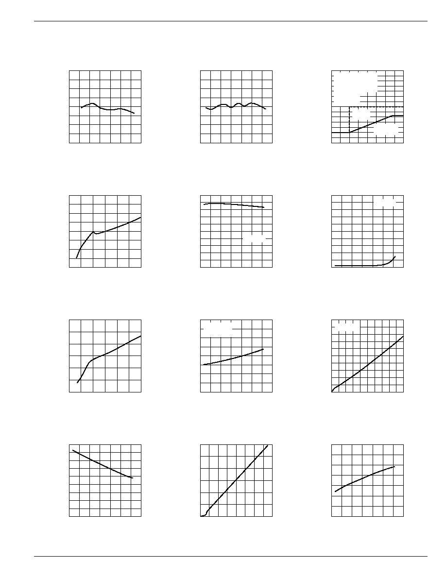
Typical Characteristics
3.26
3.27
3.28
3.29
3.30
3.31
3.32
3.33
3.34
-60 -30
0
30
60
90 120 150
OUTPUT VOLTAGE (V)
TEMPERATURE (
∞
C)
3.3V Regulator Output
Voltage vs. Temperature
4.96
4.97
4.98
4.99
5.00
5.01
5.02
5.03
5.04
-60 -30
0
30
60
90 120 150
OUTPUT VOLTAGE (V)
TEMPERATURE (
∞
C)
5.0V Regulator Output
Voltage vs. Temperature
2.0
3.0
4.0
5.0
6.0
7.0
8.0
9.0
10.0
0
5
10
15
20
25
30
ON-STATE SUPPLY CURRENT (mA)
SUPPLY VOLTAGE (V)
MIC5157/8 On-State Supply
Current vs. Supply Voltage
0.0
0.5
1.0
1.5
2.0
2.5
3.0
3.5
4.0
4.5
5.0
-60 -30
0
30
60
90 120 150
ON-STATE SUPPLY CURRENT (mA)
TEMPERATURE (
∞
C)
MIC5157/8 On-State Supply
Current vs. Temperature
V
DD
= 5V
0.0
0.5
1.0
1.5
2.0
2.5
3.0
3.5
4.0
4.5
5.0
-60 -30
0
30
60
90 120 150
OFF-STATE SUPPLY CURRENT (
µ
A)
TEMPERATURE (
∞
C)
Off-State Supply Current
vs. Temperature
V
DD
= 5V
0
10
20
30
40
50
60
0
5
10
15
20
25
30
CHARGE PUMP VOLTAGE (V)
SUPPLY VOLTAGE (V)
Charge-Pump Output Voltage
vs. Supply Voltage
0
25
50
75
100
125
150
175
200
-60 -30
0
30
60
90 120 150
FLAG VOLTAGE (mV)
TEMPERATURE (
∞
C)
Flag Output Voltage
vs. Temperature
V
DD
= 5V
I
FLAG
= 1mA
0.0
0.2
0.4
0.6
0.8
1.0
1.2
1.4
1.6
1.8
-60 -30
0
30
60
90 120 150
ENABLE THRESHOLD VOLTAGE (V)
TEMPERATURE (
∞
C)
Enable Threshold Voltage
vs. Temperature
0
10
20
30
40
50
60
70
-60 -30
0
30
60
90 120 150
CURRENT LIMIT THRESHOLD (mV)
TEMPERATURE (
∞
C)
Current Limit Threshold
vs. Temperature
-2
0
2
4
6
8
10
12
-0.2
0.0
0.2
0.4
0.6
VOLTAGE (V)
TIME (ms)
MIC5157/8 Turn-On
Response Time for 3.3V
C
CP
= 1
µ
F
C
L
= 50
µ
F
LOGIC
INPUT
3.3V
OUTPUT
MOSFET = IRF540
V
IN
= 5V, I
L
= 0.5A
C
C1
= C
C2
= 0.1
µ
F
0.0
0.1
0.2
0.3
0.4
0.5
0.6
0.7
0.8
0.9
1.0
0
2
4
6
8
10
FLAG VOLTAGE (V)
FLAG SINK CURRENT (mA)
Flag Output Voltage
vs. Flag Current
V
DD
= 5V
0
20
40
60
80
100
120
0
2
4
6
8
10 12 14 16
ENABLE BIAS CURRENT (
µ
A)
ENABLE VOLTAGE (V)
Enable Input Bias Current
vs. Enable Voltage

MIC5156/5157/5158
Micrel
MIC5156/5157/5158
6
March 1999
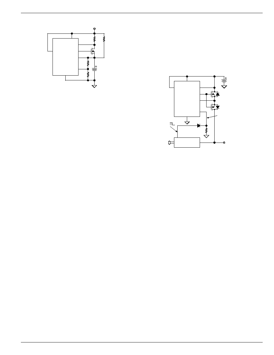
Block Diagram MIC5156
EN
Enable
Shutdown
1.235V
Bandgap
Reference
Internal
Bias
Error
Amp
75mV
35mV
GND
S* (Source)
16.6V
I
LIMIT
Comparator
D (Drain)
[I
LIMIT
]
G (Gate)
FLAG
V
P
V
DD
V
OUT
Comparator
10k
to all
internal blocks
EA
17k
Load 1
Regulated
+3.3V Output
Load 2
+12V Input
+5V Input
+5V Input
R
S
3m
0.1µF
Q2
Q1
SMP60N03-10L
Switched
5V Load
12k
* fixed version only
3.3V = 17k, 5V = 32k
adjustable version only
C
L
Block Diagram MIC5157
Block Diagram with External Components
Fixed 3.3V Power Supply with 5.0V Load Switch
Block Diagram with External Components
Fixed 3.3V 10A Power Supply
1.235V
Bandgap
Reference
V
CP
Clamp
Internal
Bias
Error
Amp
75mV
35mV
GND
S (Source)*
I
LIMIT
Comparator
D (Drain)
[I
LIMIT
]
G (Gate)
V
CP
V
DD
V
OUT
Comparator
to all
internal blocks
3.3V
Load
Regulated
+3.3V Output
+5V Input
Q1
IRFZ44
R
S
3m
1µF
16.6V
10k
58k
15k
17k
5V
Oscillator
Charge Pump
Tripler
C1+
C1≠
C2+
C2≠
0.1µF
0.1µF
C1
C2
C3
FLAG
EN
Enable
Shutdown
C
L

March 1999
7
MIC5156/5157/5158
MIC5156/5157/5158
Micrel
Functional Description
A
Super LDO Regulator is a complete regulator built around
Micrel's
Super LDO Regulator Controller.
Refer to Block Diagrams MIC5156, MIC5157, and MIC5158.
Version Differences
The MIC5156 requires an external voltage for MOSFET gate
drive and is available in 3.3V fixed output, 5V fixed output, or
adjustable output versions. With 8-pins, the MIC5156 is the
smallest of the Super LDO Regulator Controllers.
The MIC5157 and MIC5158 each have an internal charge
pump which provides MOSFET gate drive voltage. The
MIC5157 has a selectable fixed output of 3.3V, 5V, or 12V.
The MIC5158 may be configured for a fixed 5V or adjustable
output.
Enable (EN)
With at least 3.0V on V
DD
, applying a TTL low to EN places
the controller in shutdown mode. A TTL high on EN enables
the internal bias circuit which powers all internal circuitry. EN
must be pulled high if unused. The voltage applied to EN may
be as high as 36V.
The controller draws less than 1
µ
A in shutdown mode.
Gate Enhancement
The Super LDO Regulator Controller manages the gate-to-
source enhancement voltage for an external N-channel
1.235V
Bandgap
Reference
V
CP
Clamp
Internal
Bias
Error
Amp
75mV
35mV
EA
S (Source)
I
LIMIT
Comparator
D (Drain)
[I
LIMIT
]
G (Gate)
V
CP
V
DD
V
OUT
Comparator
to all
internal blocks
GND
Regulated
+3.6V Output
+5V Input
Q1
IRFZ44
R
S
3m
1µF
16.6V
32k
10k
5V
FB
Oscillator
Charge Pump
Tripler
C1+
C1≠
C2+
C2≠
0.1µF
0.1µF
C1
C2
C3
FLAG
Load
19.1k
10.0k
EN
Enable
Shutdown
C
L
Block Diagram MIC5158
Block Diagram with External Components
Adjustable Power Supply, 3.6V Configuration
MOSFET (regulator pass element) placed between the sup-
ply and the load. The gate-to-source voltage may vary from
1V to 16V depending upon the supply and load conditions.
Because the source voltage (output) approaches the drain
voltage (input) when the regulator is in dropout and the
MOSFET is fully enhanced, an additional higher supply
voltage is required to produce the necessary gate-to-source
enhancement. This higher gate drive voltage is provided by
an external gate drive supply (MIC5156) or by an internal
charge pump (MIC5157 and MIC5158).
Gate Drive Supply Voltage (MIC5156 only)
The gate drive supply voltage must not be more than 14V
above the supply voltage (V
P
≠ V
DD
< 14V). The minimum
necessary gate drive supply voltage is:
V
P
= V
OUT
+ V
GS
+ 1
where:
V
P
= gate drive supply voltage
V
OUT
= regulator output voltage
V
GS
= gate-to-source voltage for full
MOSFET gate enhancement
The error amplifier uses the gate drive supply voltage to drive
the gate of the external MOSFET. The error amplifier output
can swing to within 1V of V
P
.

MIC5156/5157/5158
Micrel
MIC5156/5157/5158
8
March 1999
Charge Pump (MIC5157/5158 only)
The charge pump tripler creates a dc voltage across reservoir
capacitor C3. External capacitors C1 and C2 provide the
necessary storage for the stages of the charge pump tripler.
The tripler's approximate dc output voltage is:
V
CP
3 (V
DD
≠ 1)
where:
V
CP
= charge pump output voltage
V
DD
= supply voltage
The V
CP
clamp circuit limits the charge pump voltage to 16V
above V
DD
by gating the charge pump oscillator ON or OFF
as required. The charge pump oscillator operates at 160kHz.
The error amplifier uses the charge pump voltage to drive the
gate of the external MOSFET. It provides a constant load of
about 1mA to the charge pump. The error amplifier output can
swing to within 1V of V
CP
.
Although the MIC5157/8 is designed to provide gate drive
using its internal charge pump, an external gate drive supply
voltage can be applied to V
CP
. When using an external gate
drive supply, V
CP
must not be forced more than 14V higher
than V
DD
.
When constant loads are driven, the ON/OFF switching of the
charge pump may be evident on the output waveform. This is
caused by the charge pump switching ON and rapidly in-
creasing the supply voltage to the error amplifier. The period
of this small charge pump excitation is determined by a
number of factors: the input voltage, the 1mA op-amp load,
any dc leakage associated with the MOSFET gate circuit, the
size of the charge pump capacitors, the size of the charge
pump reservoir capacitor, and the characteristics of the input
voltage and load. The period is lengthened by increasing the
charge pump reservoir capacitor (C3). The amplitude is
reduced by weakening the charge pump--this is accom-
plished by reducing the size of the pump capacitors (C1 and
C2). If this small burst is a problem in the application, use a
10
µ
F reservoir capacitor at C3 and 0.01
µ
F pump capacitors
at C1 and C2. Note that the recovery time to repetitive load
transients may be affected with small pump capacitors.
Gate-to-Source Clamp
A gate-to-source protective voltage clamp of 16.6V protects
the MOSFET in the event that the output voltage is suddenly
forced to zero volts. This prevents damage to the external
MOSFET during shorted load conditions. Refer to "Charge
Pump" for normal clamp circuit operation.
The source connection required by the gate-to-source clamp
is not available on the adjustable version of the MIC5156.
Output Regulation
At start-up, the error amplifier feedback voltage (EA), or
internal feedback on fixed versions, is below nominal when
compared to the internal 1.235V bandgap reference. This
forces the error amplifier output high which turns on external
MOSFET Q1. Once the output reaches regulation, the con-
troller maintains constant output voltage under changing
input and load conditions by adjusting the error amplifier
output voltage (gate enhancement voltage) according to the
feedback voltage.
Out-of-Regulation Detection
When the output voltage is 8% or more below nominal, the
open-collector FLAG output (normally high) is forced low to
signal a fault condition. The FLAG output can be used to
signal or control external circuitry. The FLAG output can also
be used to shut down the regulator using the EN control.
Current Limiting
Super LDO Regulators perform constant-current limiting (not
foldback). To implement current limiting, a sense resistor
(R
S
) must be placed in the "power" path between V
DD
and D
(drain).
If the voltage drop across the sense resistor reaches 35mV,
the current limit comparator reduces the error amplifier out-
put. The error amplifier output is decreased only enough to
reduce the output current, keeping the voltage across the
sense resistor from exceeding 35mV.
Application Information
MOSFET Selection
Standard N-channel enhancement-mode MOSFETs are ac-
ceptable for most Super LDO regulator applications.
Logic-level N-channel enhancement-mode MOSFETs may
be necessary if the external gate drive voltage is too low
(MIC5156), or the input voltage is too low, to provide ad-
equate charge pump voltage (MIC5157/8) to enhance a
standard MOSFET.
Circuit Layout
For the best voltage regulation, place the source, ground, and
error amplifier connections as close as possible to the load.
See figures (1a) and (1b).
GND
S
Load
G
MIC515x
V
IN
Figure 1a. Connections for Fixed Output

March 1999
9
MIC5156/5157/5158
MIC5156/5157/5158
Micrel
Adjustable Configurations
Micrel's MIC5156 [adjustable] and MIC5158 require an exter-
nal resistive divider to set the output voltage from 1.235V to
36V. For best results, use a 10k
resistor for R2. See
equation (1) and figure (2).
1)
R
1
= 1
◊
10
4
V
OUT
1.235
-
1
GND
S
EA*
MIC5157/8
R1
R2
10k
V
OUT
G
Figure 2. Typical Resistive Divider
Input Filter Capacitor
The Super LDO requires an input bypass capacitor for
accommodating wide changes in load current and for decou-
pling the error amplifier and charge pump. A medium to large
value low-ESR (equivalent series resistance) capacitor is
best, mounted close to the device.
Output Filter Capacitor
An output filter capacitor may be used to reduce ripple and
improve load regulation. Stable operation does not require a
large capacitor, but for transient load regulation the size of the
output capacitor may become a consideration. Common
aluminum electrolytic capacitors perform nicely; very low-
ESR capacitors are not necessary. Increased capacitance
(rather than reduced ESR) is preferred. The capacitor value
should be large enough to provide sufficient I = C
◊
dV/dt
current consistent with the required transient load regulation
quality. For a given step increase in load current, the output
voltage will drop by about dV = I
◊
dt/C, where I represents the
increase in load current over time t. This relationship as-
sumes that all output current was being supplied via the
MOSFET pass device prior to the load increase. Small
(0.01
µ
F to 10
µ
F) film capacitors parallel to the load will further
improve response to transient loads.
Some linear regulators specify a minimum required output
filter capacitance because the capacitor determines the
dominant pole of the system, and thereby stabilizes the
system. This is not the situation for the MIC5156/7/8; its
dominant pole is determined within its error amplifier.
GND
S
EA
Load
MIC5157
or
MIC5158
G
V
IN
Figure 1b. Connections for Adjustable Output
GND
Load
MIC5156
G
V
IN
EA
* Optional 16V zener diode
recommended in applications
where V
G
is greater than 18V
*
Figure 1c. MIC5156 Connections for
Adjustable Output
MOSFET Gate-to-Source Protection
When using the adjustable version of the MIC5156, an
external 16V zener diode placed from gate-to-source is
recommended for MOSFET protection. All other versions of
the Super LDO regulator controller use the internal gate-to-
source clamp.
Output Voltage Configuration
Fixed Configurations
The MIC5156-3.3 and MIC5156-5.0 are preset for 3.3V and
5.0V respectively.
The MIC5157 operates at 3.3V when the 3.3V pin is con-
nected to the S (source) pin; 5.0V when the 5.0V pin is
connected to the S pin; or 12V if the 3.3V and 5.0V pins are
open.
The MIC5158 operates at a fixed 5V (without an external
resistive divider) if the 5V FB pin is connected to EA.

MIC5156/5157/5158
Micrel
MIC5156/5157/5158
10
March 1999
Current Limiting
Current sensing requires a low-value series resistance (R
s
)
between V
DD
and D (drain). Refer to the typical applications.
The internal current-limiting circuit limits the voltage drop
across the sense resistor to 35mV. Equation (2) provides the
sense resistor value required for a given maximum current.
2)
R
S
=
35mV
I
LIM
where:
R
S
= sense resistor value
I
LIM
= maximum output current
Most current-limited applications require low-value resistors.
See
Application Hints 21 and 25 for construction hints.
Non-Current-Limited Applications
For circuits not requiring current limiting, do not use a sense
resistor between V
DD
and D (drain). See figure (3). The
controller will not limit current when it does not detect a 35mV
drop from V
DD
to D.
S
G
MIC5156
D
V
DD
V
IN
Figure 3. No Current Limit
3.3V Microprocessor Applications
For computer designs that use 3.3V microprocessors with 5V
logic, the FLAG output can be used to suppress the 5V supply
until the 3.3V output is in regulation. Refer to the external
components shown with the MIC5156 Block Diagram.
SMPS Post Regulator Application
A Super LDO regulator can be used as a post regulator for a
switch-mode power supply. The Super LDO regulator can
provide a significant reduction in peak-to-peak ripple voltage.
High-Current Switch Application
All versions of the MIC5156/7/8 may be used for current-
limited, high-current, high-side switching with or without
voltage regulation. See figure (4a). Simply leave the "S"
terminal open. A 16V zener diode from the gate to the source
of the MOSFET protects the MOSFET from overdrive during
fault conditions.
G
MIC5156-x.x
D
V
DD
V
IN
V
G
Gate Supply
Enable
Shutdown
EN
GND
R
S
Load
S
Figure 4a. High-Side Switch
If a MIC5157 or MIC5158 is used and is shutdown for a given
time, the charge pump reservoir V
CP
will bleed off. If recharg-
ing the reservoir causes an unacceptable delay in the load
reaching its operating voltage, do not use the EN pin for on/
off control. Instead, use the MIC5158, hold EN high to keep
the charge pump in continuous operation, and switch the
MOSFET on or off by overriding the error amplifier input as
shown in figure (4b).
GND
S
EA
Load
MIC5158
G
EN
Output Off
Output On
1N4148
V
IN
V
DD
Figure 4b. Fast High-Side Switch
Battery Charger Application
The MIC5158 may be used in constant-current applications
such as battery chargers. See figure (5). The regulator
supplies a constant-current (35mV
˜
R3) until the battery
approaches the float voltage:
V
FL
= 1. 235 1 +
R1
R2
where:
V
FL
= float voltage
At float voltage, the MOSFET is shut off. A trickle charge is
supplied by R4.
March 1999
11
MIC5156/5157/5158
MIC5156/5157/5158
Micrel
GND
S
EA
MIC5158
G
EN
V
IN
R1
R2
D
R3
R4
V
DD
Figure 5. Battery Charger Concept
Uninterruptible Power Supply
The MIC5157 and two N-channel MOSFETs provide battery
switching for uninterruptible power as shown in figure (6).
Two MOSFETs are placed source-to-source to prevent cur-
rent flow through their body diodes when switched off. The
Super LDO regulator is continuously enabled to achieve fast
battery switch-in. Careful attention must be paid to the ac-line
monitoring circuitry to ensure that the output voltage does not
fall below design limits while the battery is being switched in.
Line
Battery
S
G
MIC5158
D
V
DD
EN
GND
EA
1N4148
Uninterruptable
DC
D
S
D
G
S
G
MOSFET body diodes
shown for clarity
Off-line
Power Supply
AC
Line
Q1
Q2
40V max.
Figure 6. UPS Power Supply Concept
MIC5156/5157/5158
Micrel
MIC5156/5157/5158
12
March 1999
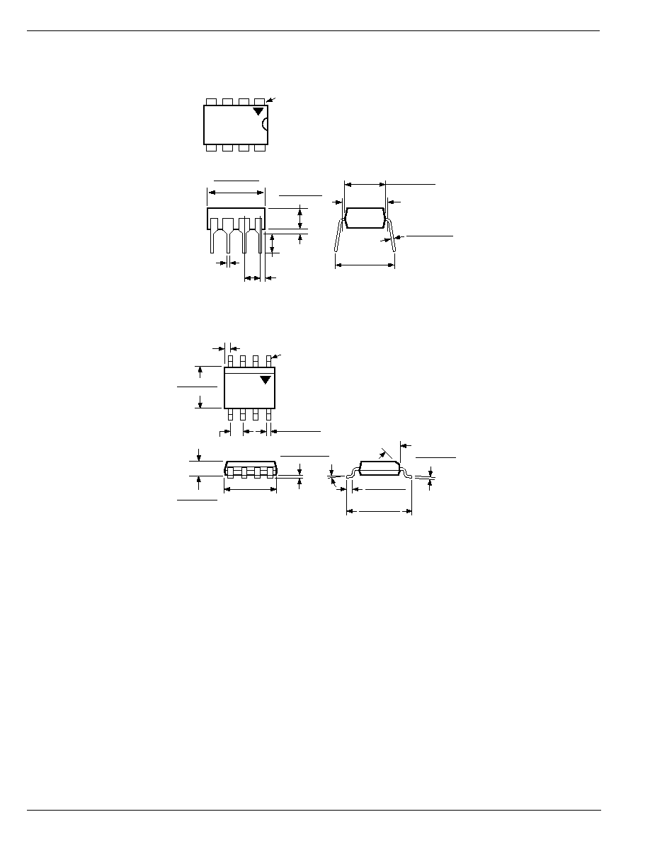
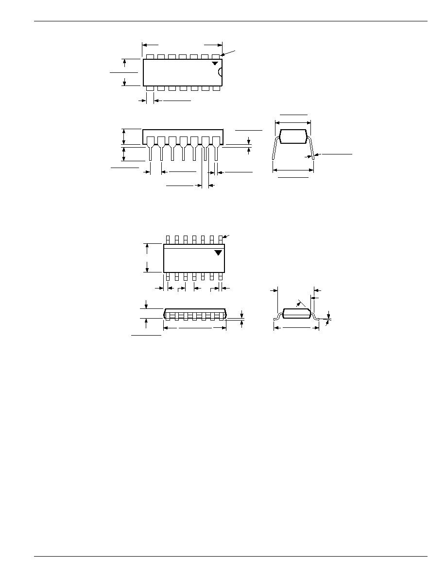
Package Information
0.380 (9.65)
0.370 (9.40)
0.135 (3.43)
0.125 (3.18)
PIN 1
DIMENSIONS:
INCH (MM)
0.018 (0.57)
0.100 (2.54)
0.013 (0.330)
0.010 (0.254)
0.300 (7.62)
0.255 (6.48)
0.245 (6.22)
0.380 (9.65)
0.320 (8.13)
0.0375 (0.952)
0.130 (3.30)
8-Pin DIP (N)
45
∞
0
∞
≠8
∞
0.244 (6.20)
0.228 (5.79)
0.197 (5.0)
0.189 (4.8)
SEATING
PLANE
0.026 (0.65)
MAX
)
0.010 (0.25)
0.007 (0.18)
0.064 (1.63)
0.045 (1.14)
0.0098 (0.249)
0.0040 (0.102)
0.020 (0.51)
0.013 (0.33)
0.157 (3.99)
0.150 (3.81)
0.050 (1.27)
TYP
PIN 1
DIMENSIONS:
INCHES (MM)
0.050 (1.27)
0.016 (0.40)
8-Pin SOP (M)
March 1999
13
MIC5156/5157/5158
MIC5156/5157/5158
Micrel
.080 (1.524)
.015 (0.381)
.023 (.5842)
.015 (.3810)
.310 (7.874)
.280 (7.112)
.770 (19.558) MAX
.235 (5.969)
.215 (5.461)
.060 (1.524)
.045 (1.143)
.160 MAX
(4.064)
.160 (4.064)
.100 (2.540)
.110 (2.794)
.090 (2.296)
.400 (10.180)
.330 (8.362)
.015 (0.381)
.008 (0.2032)
.060 (1.524)
.045 (1.143)
PIN 1
14-Pin DIP (N)
45
∞
3
∞
≠6
∞
0.244 (6.20)
0.228 (5.80)
0.344 (8.75)
0.337 (8.55)
0.006 (0.15)
SEATING
PLANE
0.026 (0.65)
MAX
)
0.016 (0.40)
TYP
0.154 (3.90)
0.057 (1.45)
0.049 (1.25)
0.193 (4.90)
0.050 (1.27)
TYP
PIN 1
DIMENSIONS:
INCHES (MM)
14-Pin SOP (M)

MIC5156/5157/5158
Micrel
MIC5156/5157/5158
14
March 1999

March 1999
15
MIC5156/5157/5158
MIC5156/5157/5158
Micrel

MIC5156/5157/5158
Micrel
MIC5156/5157/5158
16
March 1999
MICREL INC.
1849 FORTUNE DRIVE
SAN JOSE, CA 95131
USA
TEL
+ 1 (408) 944-0800
FAX
+ 1 (408) 944-0970
WEB
http://www.micrel.com
This information is believed to be accurate and reliable, however no responsibility is assumed by Micrel for its use nor for any infringement of patents or
other rights of third parties resulting from its use. No license is granted by implication or otherwise under any patent or patent right of Micrel Inc.
© 1999 Micrel Incorporated