BA210 MIC5159 Apr04
April 2004
1
M9999-041204
MIC5159
Micrel
MIC5159
Programmable Current Limit
µ
Cap LDO Regulator Controller
Micrel, Inc. · 1849 Fortune Drive · San Jose, CA 95131 · USA · tel + 1 (408) 944-0800 · fax + 1 (408) 944-0970 · http://www.micrel.com
Ordering Information
Part Number
Voltage
Marking
Junction Temp. Range
Package
MIC5159BM6
ADJ.
LZAA
40
°
C to +125
°
C
SOT-23-6
MIC5159-1.8BM6
1.8V
LZ18
40
°
C to +125
°
C
SOT-23-6
MIC5159-3.0BM6
3.0V
LZ30
40
°
C to +125
°
C
SOT-23-6
Other voltages available. Contact Micrel for details.
General Description
Micrel's MIC5159 is a precision-voltage regulator controller.
Used with an external P-Channel MOSFET, the MIC5159
forms a two-chip low-dropout regulator capable of driving a
wide range of output currents.
The MIC5159 operates from an input of 1.65V to 5.5V. The
low input voltage allows the MIC5159 to operate off of high
power 1.8V rails to generate lower voltages such as 1.5V.
Features of the MIC5159 include enable input and current-
limit protection. As a
µ
Cap design, the MIC5159 is stable with
ceramic output capacitors.
The MIC5159 is packaged in the IttyBitty
®
SOT-23-6, and is
offered in fixed and adjustable output voltages. Junction
temperature range of the MIC5159 is from 40
°
C to +125
°
C.
Features
· Fast transient response
· Input voltage range: V
IN
1.65V to 5.5V
·
±
1.0% initial output tolerance
· Fixed 1.8V or adjustable output voltage down to 1.25V
· Stable with ceramic output capacitor
· Capable up to 10A
· Excellent line and load regulation specifications
· Logic-controlled shutdown
· Programmable current limit
· Current-limit protection
· IttyBitty
®
SOT-23-6 package
· Available temperature range: 40
°
C to +125
°
C
Applications
· Ultra-high current, ultra-low dropout voltage regulator
· High-efficiency linear power supplies
· Low-voltage distributed power
· Fixed telecom
· Multimedia and PC power supplies
· Battery chargers
· Low-voltage DSP, microprocessor and microcontroller
power supplies
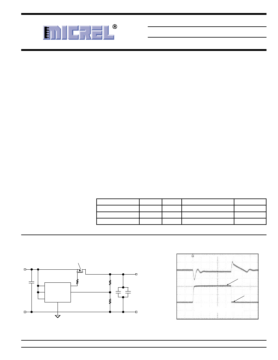
Typical Application
GATE
EN
FB
V
IN
IN
IS
V
OUT
GND
U1 MIC5159BM6
Q1ÐQ4
SUB15P01Ð52 ´ 4
R1
5
1
3
GND
C1
R2
GND
C1
C1
Adjustable Output Voltage
Load Transient Response
TIME (20
µ
s/div.)
OUTPUT CURRENT
(5A/div
.)
OUTPUT V
O
L
T
A
G
E
(100mV/div
.)
V
IN
= 3.3V
V
OUT
= 2.5V
C
OUT
= 200
µ
F
10A
100mA
IttyBitty is a registered trademark of Micrel, Inc.
MIC5159
Micrel
M9999-041204
2
April 2004
Pin Description
Pin Number
Pin Name
Pin Function
1
IN
Input Voltage.
2
GND
Ground.
3
IS
Current Sense: IS must be tied to VIN pin if the current limit feature is not
used.
4
GATE
Gate drive of the external P-Channel MOSFET.
5
EN
Enable Input: Logic Level ON/OFF control. Logic high = ON;
logic low = OFF.
6
ADJ.
Adjustable Regulator Feedback Input: Connect to resistor voltage divider.
VO
Output Voltage: Connect to drain of P-Channel MOSFET to regulate output
to proper voltage.
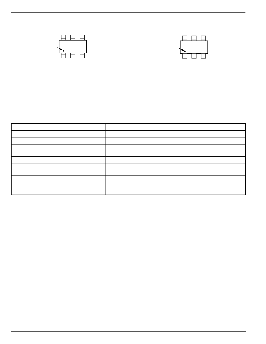
Pin Configuration
IN GND
GATE
IS
1
3
4
6
ADJ
LZAA
5
EN
2
Pin 1
Index
SOT-23-6 (M6)
Adjustable Voltage Version
IN GND
GATE
IS
1
3
4
6
VO
LZxx
5
EN
2
Pin 1
Index
SOT-23-6 (M6)
Fixed Voltage Version
April 2004
3
M9999-041204
MIC5159
Micrel
Electrical Characteristics
(4)
T
A
= 25
°
C with V
IN
= V
OUT
+ 1V; V
EN
= 1.2V, C
IN
= C
OUT
= 10
µ
F, ceramic, I
OUT
= 10mA; bold values indicate 40
°
C < T
J
< +125
°
C;
unless otherwise specified, Note 3
Parameter
Condition
Min
Typ
Max
Units
Output Voltage Accuracy
At 25
°
C
1
+1
%
Over temperature range
2
+2
%
Output Voltage Line Regulation
V
IN
= V
OUT
+ 1.0V to 5.5V
0.1
0.007
+0.1
%/V
Output Voltage Load Regulation
I
L
= 10mA to 1.0A
0.2
1.0
%
Ground Pin Current
(6)
V
EN
0.2V (MIC5159 OFF)
15
30
µ
A
V
EN
1.2V (MIC5159 ON)
10
20
mA
Adjust Pin Bias Current
1
µ
A
Maximum V
GS
(PFET fully ON); V
IN
= 5.0V
4.5
V
(PFET fully ON); V
IN
= 3.3V
3.1
V
(PFET fully ON); V
IN
= 2.5V
2.3
V
Current-Limit Threshold
V
IN
V
IS
40
50
65
mV
Start-up Time
V
EN
= V
IN
30
150
µ
s
Enable Input
Enable Input Threshold
Regulator enabled
1.2
V
Regulator shutdown
0.2
V
Enable hysteresis
20
50
250
mV
Enable Pin Input Current
Independent of state
0.01
nA
1
µ
A
Notes:
1. Exceeding the absolute maximum rating may damage the device.
2. The device is not guaranteed to function outside its operating rating.
3. P
D
(max) = (T
J
(max) T
A
)
÷
JA
, where
JA
depends upon the printed circuit layout, see "Applications Information."
4. Devices are ESD sensitive. Handling precautions recommended. Human body model, 1.5k in series with 100pF.
5. Specification for packaged product only.
6. I
GND
is the quiescent current. I
IN
= I
GND
+ I
OUT
.
Absolute Maximum Ratings
(1)
Supply Voltage (V
IN
) .................................................. +6.0V
Enable Input Voltage (V
EN
) ........................................ +6.0V
Power Dissipation (P
D
(max)) ................................... Note 3
Storage Temperature (T
S
) ....................... 65
°
C to +150
°
C
Lead Temperature (soldering, 5 sec.) ....................... 260
°
C
ESD Rating
(4)
................................................................ 2kV
Operating Ratings
(2)
Supply Voltage (V
IN
) ................................. +1.65V to +5.5V
Enable Input Voltage (V
EN
) .............................. 0V to +5.5V
Junction Temperature (T
J
) ................ 40
°
C
T
J
+125
°
C
Package Thermal Resistance
SOT-23-6 (
JA
) .............................................. 235
°
C/W
MIC5159
Micrel
M9999-041204
4
April 2004
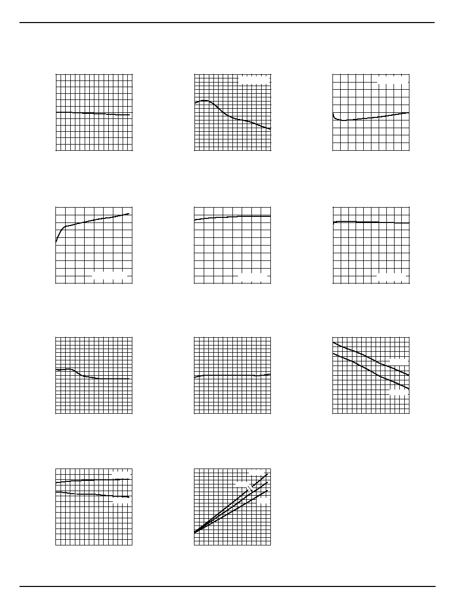
Typical Characteristics
1.22
1.225
1.23
1.235
1.24
1.245
1.25
1.65
2.15
2.65
3.15
3.65
4.15
4.65
5.15
5.65
REFERENCE VOLTAGE (V)
INPUT VOLTAGE (V)
Reference Voltage
vs. Input Voltage
1.23
1.231
1.232
1.233
1.234
1.235
1.236
1.237
1.238
1.239
1.24
-40 -20 0
20 40 60 80 100 120
REFERENCE VOLTAGE (V)
TEMPERATURE (
°
C)
Reference Voltage
vs. Temperature
V
IN
= 3.3V
1.23
1.231
1.232
1.233
1.234
1.235
1.236
1.237
1.238
1.239
1.24
0 0.5 1 1.5 2 2.5 3 3.5 4 4.5 5
OUTPUT VOLTAGE (V)
LOAD (A)
Output Voltage
vs. Load
V
IN
= 2.5V
0
1
2
3
4
5
6
7
8
9
10
1.65
2.15
2.65
3.15
3.65
4.15
4.65
5.15
5.65
QUIESCENT CURRENT (mA)
INPUT VOLTAGE (V)
Quiescent Current
vs. Input Voltage
I
LOAD
= 10mA
0
1
2
3
4
5
6
7
8
9
10
-40 -20 0
20 40 60 80 100 120
QUIESCENT CURRENT (mA)
TEMPERATURE (
°
C)
Quiescent Current
vs. Temperature
V
IN
= 3.3V
0
1
2
3
4
5
6
7
8
9
10
0 0.5 1 1.5 2 2.5 3 3.5 4 4.5 5
QUIESCENT CURRENT (mA)
LOAD (A)
Quiescent Current
vs. Load
V
IN
= 2.5V
40
42
44
46
48
50
52
54
56
58
60
1.65
2.15
2.65
3.15
3.65
4.15
4.65
5.15
5.65
CURRENT LIMIT THRESHOLD (mV)
INPUT VOLTAGE (V)
Current Limit Threshold
vs. Input Voltage
40
42
44
46
48
50
52
54
56
58
60
-40 -20 0
20 40 60 80 100 120
CURRENT LIMIT THRESHOLD (mV)
TEMPERATURE (
°
C)
Current Limit Threshold
vs. Temperature
0
100
200
300
400
500
600
700
800
-40 -20 0
20 40 60 80 100 120
ENABLE THRESHOLD (mV)
TEMPERATURE (
°
C)
Enable Threshold
vs. Temperature
EN on
EN off
0
100
200
300
400
500
600
700
1.65
2.15
2.65
3.15
3.65
4.15
4.65
5.15
5.65
ENABLE THRESHOLD (mV)
INPUT VOLTAGE (V)
Enable Threshold
vs. Input Voltage
EN on
EN off
0
2
4
6
8
10
12
14
16
18
20
1.65
2.15
2.65
3.15
3.65
4.15
4.65
5.15
5.65
SHUTDOWN CURRENT (
µ
A)
INPUT VOLTAGE (V)
Shutdown Current
vs. Input Voltage
85
°
C
25
°
C
-40
°
C
April 2004
5
M9999-041204
MIC5159
Micrel
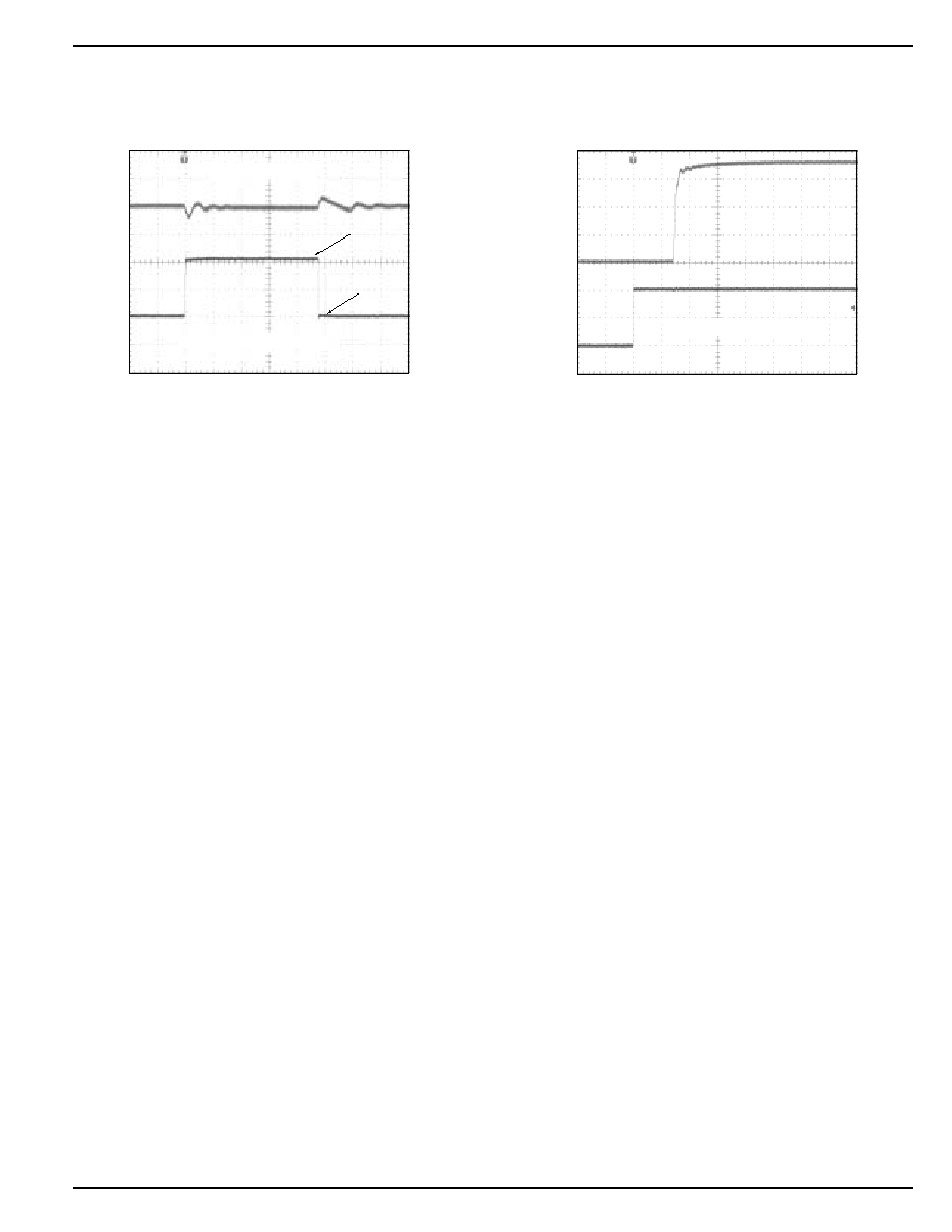
Functional Characteristics
Load Transient Response
TIME (20
µ
s/div.)
OUTPUT CURRENT
(1A/div
.)
OUTPUT V
O
L
T
A
G
E
(100mV/div
.)
V
IN
= 1.8V
V
OUT
= 1.5V
C
OUT
= 100
µ
F
2A
10mA
Enable Characteristics
TIME (20
µ
s/div.)
ENABLE VOL
T
AGE
(1V/div
.)
OUTPUT
VOL
T
AGE
(100mV/div
.)
V
IN
= 3.3V
V
OUT
= 1.8V