
February 2005
1
M9999-092004
MIC5162
Micrel, Inc.
MIC5162
Dual Regulator Controller For High-Speed Bus Termination
General Description
The MIC5162 is a dual regulator controller designed for high-
speed bus termination. It offers a simple, low-cost JEDEC
compliant solution for terminating high-speed, low-voltage
digital buses (i.e. DDR, SCSI, GTL, SSTL, HSTL, LV-TTL,
Rambus, LV-PECL, LV-ECL, etc).
The MIC5162 controls two external N-Channel MOSFETs to
form two separate regulators. It operates by switching be-
tween either the high-side MOSFET or the low-side MOSFET
depending on whether the current is being sourced to the load
or sinked by the regulator.
Designed to provide a universal solution for bus termination
regardless of input voltage, output voltage, or load current,
the desired MIC5162 output voltage can be programmed by
externally forcing the reference voltage.
The MIC5162 operates from an input of 1.35V to 6V, with a
second bias supply input required for operation. It is available
in the tiny MSOP-10 package with operating junction tem-
perature range of ≠40∞C to +125∞C.
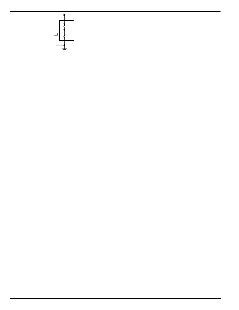
Typical Application
Features
∑ JEDEC Compliant Bus Termination for SCSI, GTL,
SSTL, HSTL, LV-TTL, Rambus, LV-PECL, LV-ECL, etc.
∑ DDR memory termination
∑ Tracking programmable output
∑ Requires minimal external components
∑ Wide bandwidth
∑ Input voltage range: 1.35V to 6V
∑ Logic controlled enable input
∑ Tiny MSOP-10 package
∑ Available ≠40∞C < T
J
< +125∞C
Applications
∑ Desktop computers
∑ Notebook computers
∑ Communication systems
∑ Video cards
Micrel, Inc. ∑ 2180 Fortune Drive ∑ San Jose, CA 95131 ∑ USA ∑ tel + 1 (408) 944-0800 ∑ fax + 1 (408) 474-1000 ∑ http://www.micrel.com
Load Transient
TIME (200µs/div)
V
TT ≠
V
REF
(50mV/div)
SOURCE
(2A/div)
Source 3A
0A
Sink 3A
Typical SSTL-2 Application
C
OUT
= 330µF
EN
220pF
3k
V
CC
= 5.0V
V
DDQ
= 1.35V
to 6.0V
V
TT
=
1
/
2
V
DDQ
SUD50N02-06
MIC5162BMM
VDDQ
VCC
VREF
HD
COMP
EN
LD
FB
GND
120pF
V
IN
=2.5V to 1.5V
Ordering Information
Part Number
Junction
Standard
Pb-Free
Temp Range
Package
MIC5162BMM
MIC5162YMM
≠40∞C to +125∞C
10-Pin MSOP

MIC5162
Micrel, Inc.
M9999-092004
2
February 2005
Pin Description
Pin Number
Pin Name
Pin Function
1
VCC
Bias Supply Input. Apply 5V to this input for internal bias to the controller.
2
EN
Enable (Input): CMOS compatible input. Logic high = enable, logic low =
shutdown.
3
VDDQ
Input supply voltage.
4
VREF
Reference output equal to half of V
DDQ
.
5
GND
Ground.
6
FB
Feedback input to the to the internal error amplifier.
7
Comp
Compensation (Output): Connect a capacitor to feedback pin for compensa-
tion of the internal control loop.
8
LD
Low-side drive: Connects to the Gate of the external low side MOSFET.
9
HD
High-side drive: Connects to the Gate of the external high side MOSFET.
10
N/C
Not internally connected.
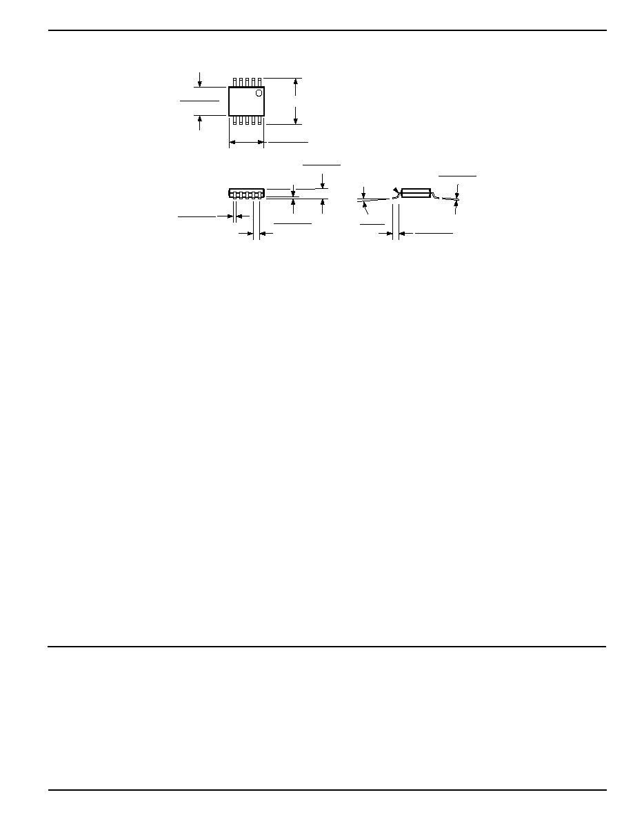
Pin Configuration
GND
FB
6
5
1
VCC
EN
VDDQ
VREF
10 N/C
HD
LD
COMP
9
8
7
2
3
4
10-Lead MSOP
February 2005
3
M9999-092004
MIC5162
Micrel, Inc.
Electrical Characteristics
T
A
= 25∞C with V
DDQ
= 2.5V; V
CC
= 5V; V
EN
= V
CC
; bold values indicate ≠40∫C<T
J
<+125∫C; unless otherwise specified. See test
circuit 1 for test circuit configuration.
Parameter
Condition
Min
Typ
Max
Units
V
REF
Voltage
≠1%
0.5V
DDQ
1%
V
V
TT
Voltage Accuracy (Note 2)
Sourcing; 100mA to 3A
≠5
0.4
5
mV
≠10
≠10
Sinking; ≠100mA to ≠3A
≠5
0.6
5
mV
≠10
10
Supply Current (I
DDQ
)
V
EN
= 1.2V (controller ON)
120
140
µA
No Load
200
Supply Current (I
CC
)
No Load
15
20
mA
25
I
CC
Shutdown Current (Note 3)
V
EN
= 0.2V (controller OFF)
10
35
µA
Start≠up Time (Note 4)
V
CC
, = 5V external bias; V
EN
= V
IN
8
15
µs
30
Enable Input
Enable Input Threshold
Regulator enable
1.2
V
Regulator shutdown
0.3
V
Enable Hysteresis
40
mV
Enable Pin Input Current
V
IL
< 0.2V (controller shutdown)
0.01
µA
V
IH
> 1.2V (controller enabled)
5.5
µA
Drive
High Side Gate Drive Voltage
High Side MOSFET Fully ON
4.8
4.97
V
High Side Gate Drive Voltage
High Side MOSFET Fully OFF
0.03
0.2
V
Low Side Gate Drive Voltage
Low Side MOSFET Fully ON
4.8
4.97
V
Low Side Gate Drive Voltage
Low Side MOSFET Fully OFF
0.03
0.2
V
Note 1.
Exceeding the absolute maximum ratings may damage the device.
Note 2.
The V
TT
voltage accuracy is measured as a delta voltage from the reference output (V
TT
≠ V
REF
).
Note 3.
Shutdown current is measured only on the V
CC
pin. The V
DDQ
pin will always draw a minimum amount of current when voltage is applied.
Note 4.
Start-up time is defined as the amount of time from V
EN
= V
CC
to HSD = 90% of V
CC
.
Absolute Maximum Ratings
(Note 1)
Supply Voltage (V
CC
) ...................................................... 7V
Supply Voltage (V
DDQ
) .................................................... 7V
Enable Input Voltage (V
EN
) ............................................. 7V
Junction Temperature Range ............ ≠40∞C < T
J
< +125∞C
Operating Ratings
(Note 2)
Supply Voltage (V
CC
) ............................................ 3V to 6V
Supply Voltage (V
DDQ
) ....................................... 1.35V - 6V
Enable Input Voltage (V
EN
) .................................. 0V to VIN

MIC5162
Micrel, Inc.
M9999-092004
4
February 2005
Test Circuit
C
OUT
= 3 ◊ 560µF
10k
EN
470pF
10µF
220µF
V
CC
= 5.0V
V
DDQ
= 1.8V
or 2.5V
V
TT
SUD50N02-06
MIC5162BMM
VDDQ
VCC
HD
COMP
EN
LD
VREF
FB
GND
120pF
Figure 1. Test Circuit
February 2005
5
M9999-092004
MIC5162
Micrel, Inc.
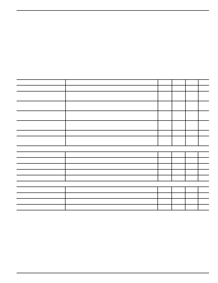
Typical Characteristics
-5
-4
-3
-2
-1
0
1
2
3
4
5
-3
-2
-1
0
1
2
3
[V
TT
≠V
REF
] (mV)
OUTPUT CURRENT (A)
[V
TT
≠V
REF
]
vs. Output Current
-10
-8
-6
-4
-2
0
2
4
6
8
10
-40 -20 0
20 40 60 80 100 120
[V
TT
≠V
REF
] (mV)
TEMPERATURE (∞C)
[V
TT
≠V
REF
]
vs. Temperature
SINK 3A
-10
-8
-6
-4
-2
0
2
4
6
8
10
-40 -20 0
20 40 60 80 100 120
[V
TT
≠V
REF
] (mV)
TEMPERATURE (∞C)
[V
TT
≠V
REF
]
vs. Temperature
SOURCE 3A
1.2375
1.2400
1.2425
1.2450
1.2475
1.2500
1.2525
1.2550
1.2575
1.2600
1.2625
-40 -20 0
20 40 60 80 100 120
V
REF
(V)
TEMPERATURE (∞C)
V
REF
vs. Temperature
V
DDQ
= 2.5V
0
2
4
6
8
10
12
14
16
18
0
1
2
3
4
5
6
SOURCE CURRENT (mA)
INPUT VOLTAGE (V)
V
CC
Current
vs. Input Voltage
0
2
4
6
8
10
12
14
16
18
20
-40 -20 0
20 40 60 80 100 120
SOURCE CURRENT (mA)
TEMPERATURE (∞C)
V
CC
Current
vs. Temperature
V
CC
= 5V
MIC5162
Micrel, Inc.
M9999-092004
6
February 2005
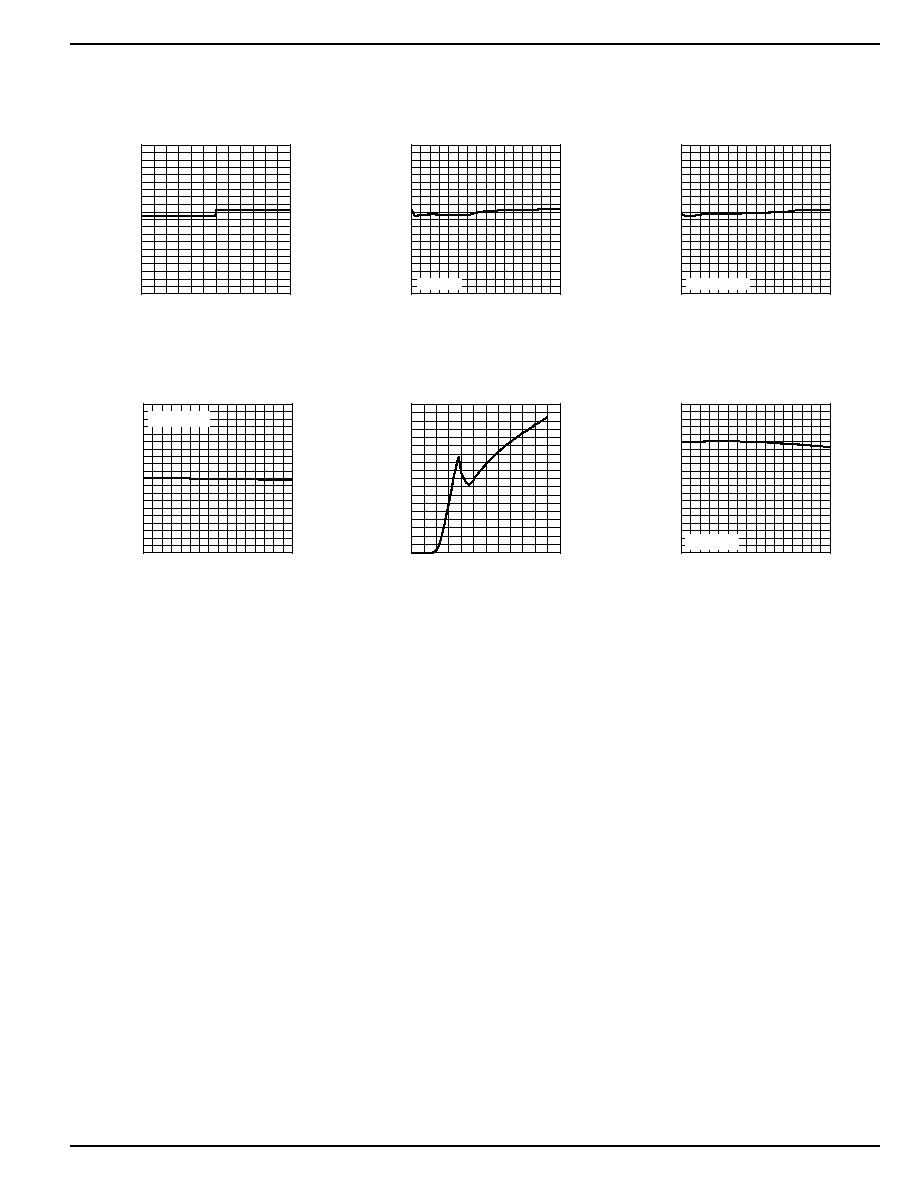
Functional Diagram
Shutdown
COMP
FB
GND
V
DDQ
V
CC
V
REF
EN
LD
HD
R1
R2
A
≠A
Block Diagram
February 2005
7
M9999-092004
MIC5162
Micrel, Inc.
Applications Information
High performance memory requires high speed signaling.
This increase in speed requires special attention to maintain
signal integrity. Bus termination provides a means to in-
crease signaling speed while maintaining good signal integ-
rity. An example of bus termination is the Series Stub Termi-
nation Logic or SSTL. Figure 1 is an example of an SSTL 2
single ended series parallel terminated output. SSTL 2 is a
JEDEC signaling standard operating off of a 2.5V supply. It
consists of a series resistor (R
S
) and a terminating resistor
(R
T
). Values of R
S
will range between 10 to 30 with a
typical of 22, while R
T
will range from 22 to 28 with a
typical value of 25. V
REF
must maintain 1/2 V
DD
with a ±1%
tolerance, while V
TT
will dynamically sink and source current
to maintain a termination voltage of ±40mV from the V
REF
line
under all conditions. This method of bus termination reduces
common mode noise, settling time, voltage swings, EMI/RFI
and improves slew rates.
V
DDQ
VREF
R
S
R
T
V
TT
MEMORY
Figure 1.
The MIC5162 is a high performance linear controller, utilizing
scalable N-Channel MOSFETs to provide JEDEC compliant
bus termination. Termination is achieved by dividing down
the V
DDQ
voltage by half, providing the reference (V
REF
)
voltage. An internal error amplifier compares the termination
voltage (V
TT
) and V
REF
, controlling 2 external N-Channel
MOSFETs to sink and/or source current to maintain a termi-
nation voltage (V
TT
) equal to V
REF
. The N-Channels receive
their enhancement voltage from a separate V
CC
pin on the
device.
Although the general discussion is focused on SSTL, the
MIC5162 is also capable of providing bus terminations for
SCSI, GTL, HSTL, LV-TTL, Rambus, LV-PECL and other
systems.
V
DDQ
The V
DDQ
pin on the MIC5162 provides the source current
through the high side N-Channel and the reference voltage to
the device. The MIC5162 can operate at V
DDQ
voltages as
low as 1.35V. Due to the possibility of large transient currents
being sourced from this line, significant bypass capacitance
will aid in performance by improving the source impedance at
higher frequencies. Since the reference is simply V
DDQ
/2,
perturbations on the V
DDQ
will also appear at half the ampli-
tude on the reference. For this reason, low ESR capacitors
such as ceramics or Oscons are recommended on V
DDQ
.
V
TT
V
TT
is the actual termination point. V
TT
is regulated to V
REF
.
Due to high speed signaling, the load current seen by V
TT
is
constantly changing. To maintain adequate large signal
transient response, large Oscons ceramics are recommended
on V
TT
. The proper combination and placement of the Oscon
and ceramic capacitors is important to reduce both ESR and
ESL such that high-current high-speed transients do not
exceed the dynamic voltage tolerance requirement of V
TT
.
The larger Oscon capacitors provide bulk charge storage
while the smaller ceramic capacitors provide current during
the fast edges of the bus transition. Using several smaller
ceramic capacitors distributed near the termination resistors
is typically important to reduce the effects of PCB trace
inductance.
V
REF
Two resistors dividing down the V
DDQ
voltage provide V
REF
(Figure 3). The resistors are valued at around 17k. A
minimum capacitor value of 120pF from V
REF
to ground is
required to remove high frequency signals reflected from the
source. Large capacitance values (>1500pF) should be
avoided. Values greater than 1500pF slow down V
REF
and
detract from the reference voltage's ability to track V
DDQ
during high speed load transients.
330µF
Oscon
Vishay
SUD50N02-06
120pF
1µF
Ceramic
100µF
Oscon
3k
Vishay
SUD50N02-06
MIC5162BMM
VDDQ
VCC
HD
VREF
LD
COMP
GND
FB
220pF
Figure 2.
MIC5162
Micrel, Inc.
M9999-092004
8
February 2005
120pF
VDDQ
VREF
GND
Figure 3.
V
REF
can also be manipulated for different applications. A
separate voltage source can be used to externally set the
reference point, bypassing the divider network. Also, external
resistors can be added from V
REF
to ground or V
REF
to V
DDQ
to shift the reference point up or down.
V
CC
V
CC
supplies the internal circuitry of the MIC5162 and pro-
vides the drive voltage to enhance the external N-Channel
MOSFETs. A small 1µF capacitor is recommended for by-
passing the V
CC
pin. The minimum V
CC
voltage should be a
gate-source voltage above V
TT
without exceeding 6V. For
example, on an SSTL compliant terminator, V
DDQ
equals
2.5V and V
TT
equals 1.25V. If the N-Channel MOSFET
selected requires a gate source voltage of 2.5V, V
CC
should
be a minimum of 3.75V.
Feedback and Compensation
The feedback provides the path for the error amplifier to
regulate V
TT
. An external resistor must be placed between
the feedback and V
TT
. This allows the error amplifier to be
correctly externally compensated.
For most applications, a 3k resistor is recommended.
The COMP pin on the MIC5162 is the output of the internal
error amplifier. By placing a capacitor between the COMP pin
and the feedback pin, this coupled with the feedback resistor
places an external pole on the error amplifier. With a 3k
feedback resistor, a minimum 220pF capacitor is recom-
mended for a 3A peak termination circuit. Increases in load,
multiple N-Channel MOSFETs and/or increase in output
capacitance may require feedback and/or compensation
capacitor values to be increased to maintain stability. Feed-
back resistor values should not exceed 100k and compen-
sation capacitors should not be less than 40pF.
Enable
The MIC5162 features an active high enable input. In the off
mode state, leakage currents are reduced to microamperes.
The enable input has thresholds compatible with TTL/CMOS
for simple logic interfacing. The enable pin can be tied directly
to V
DDQ
or V
CC
for functionality. Do not float the enable pin.
Floating this pin causes the enable to be in an indeterminate
state.
Input Capacitance
Although the MIC5162 does not require an input capacitor for
stability, using one greatly improves device performance.
Due to the high-speed nature of the MIC5162, low ESR
capacitors such as Oscon and ceramics are recommended
for bypassing the input. The recommended value of capaci-
tance will depend greatly on the proximity to the bulk capaci-
tance. Although a 10µF ceramic capacitor will suffice for most
applications, input capacitance may need to be increased in
cases where the termination circuit is greater than 1" away
from the bulk capacitance.
Output Capacitance
Large, low ESR capacitors are recommended for the output
(V
TT
) of the MIC5162. Although low ESR capacitors are not
required for stability, they are recommended to reduce the
effects of high-speed current transients on V
TT
. The change
in voltage during the transient condition will be the effect of the
peak current multiplied by the output capacitor's ESR. For
that reason, Oscon type capacitors are excellent for this
application. They have extremely low ESR and large capaci-
tance-to-size ratio. Ceramic capacitors are also well suited to
termination due to their low ESR. These capacitors should
have a dielectric rating of X5R or X7R. Y5V and Z5U type
capacitors are not recommended, due to their poor perfor-
mance at high frequencies and over temperature. The mini-
mum recommended capacitance for a 3 amp peak circuit is
100µF. Output capacitance can be increased to achieve
greater transient performance.
MOSFET Selection
The MIC5162 utilizes external N-Channel MOSFETs to sink
and source current. MOSFET selection will settle to two main
categories: size and gate threshold (V
GS
).
MOSFET Power Requirements
One of the most important factors is to determine the amount
of power the MOSFET is going to be required to dissipate.
Power dissipation in an SSTL circuit will be identical for both
the high side and low side MOSFETs. Since the supply
voltage is divided by half to supply V
TT
, both MOSFETs have
the same voltage dropped across them. They are also
required to be able to sink and source the same amount of
current (for either all 0's or all 1's). This equates to each side
being able to dissipate the same amount of power. Power
dissipation calculation for the high-side driver is as follows:
P
V
V
I SOURCE
D
DDQ
TT
=
-
(
)
◊ _
Where I_source is the average source current.
Power dissipation for the low-side MOSFET is as follows;
P
V
I SINK
D
TT
=
◊ _
Where I_sink is the average sink current.
In a typical 3 amp peak SSTL_2 circuit, power considerations
for MOSFET selection would occur as follows.
P
V
V
I SOURCE
P
V
V
A
P
W
D
DDQ
TT
D
D
=
-
(
)
◊
=
-
(
)
◊
=
_
.
.
.
2 5
1 25
1 6
2
This typical SSTL_2 application would require both high-side
and low-side N-Channel MOSFETs to be able to handle 2
Watts each. In applications where there is excessive power
dissipation, multiple N-Channel MOSFETs may be placed in
parallel. These MOSFETs will share current, distributing
power dissipation across each device.

February 2005
9
M9999-092004
MIC5162
Micrel, Inc.
The maximum MOSFET die (junction) temperature limits
maximum power dissipation. The ability of the device to
dissipate heat away from the junction is specified by the
junction-to-ambient (
JA
) thermal resistance. This is the sum
of junction-to-case (
JC
) thermal resistance, case-to-sink
(
CA
) thermal resistance and sink-to-ambient (
SA
) thermal
resistance;
JA
JC
CS
SA
=
+
+
In our example of a 3A peak SSTL_2 termination circuit, we
have selected a D-pack N-Channel MOSFET that has a
maximum junction temperature of 150∞C. The device has a
junction-to-case thermal resistance of 1.5∞C/Watt. Our appli-
cation has a maximum ambient temperature of 60∞C. The
required junction-to-ambient thermal resistance can be cal-
culated as follows;
JA
J
A
D
T
T
P
=
-
Where T
J
is the maximum junction temperature, T
A
is the
maximum ambient temperature and P
D
is the power dissipa-
tion.
In our example;
JA
J
A
D
JA
JA
T
T
P
C
C
W
C W
=
-
=
∞ -
∞
=
∞
150
60
2
45
/
This shows that our total thermal resistance must be better
than 45∞C/W. Since the total thermal resistance is a combi-
nation of all the individual thermal resistances, the amount of
heat sink required can be calculated as follows;
SA
JA
JC
CA
=
-
+
(
)
In our example;
SA
SA
C W
C W
C W
C W
=
∞
-
∞
+
∞
(
)
=
∞
45
1 5
0 5
43
/
.
/
.
/
/
In most cases, case-to-sink thermal resistance can be as-
sumed to be about 0.5∞C/W.
The SSTL termination circuit for our example, using 2 D-pack
N-Channel MOSFETs (one high side and one on the low side)
will require at least a 43∞C/W heat sink per MOSFET. This
may be accomplished with an external heat sink or even just
the copper area that the MOSFET is soldered to. In some
cases, airflow may also be required to reduce thermal resis-
tance.
MOSFET Gate Threshold
N-Channel MOSFETs require an enhancement voltage
greater than its source voltage. Typical N-Channel MOS-
FETs have a gate-source threshold (V
GS
) of 1.8V and higher.
Since the source of the high side N-Channel is connected to
V
TT
, the MIC5162 V
CC
pin requires a voltage equal to or
greater than the V
GS
voltage. For example, our SSTL_2
termination circuit has a V
TT
voltage of 1.25V. For an N-
Channel that has a V
GS
rating of 2.5V, the V
CC
voltage can
be as low as 3.75V. With an N-Channel that has a 4.5V V
GS
,
the minimum V
CC
required is 5.75V. Although these N-
Channels are driven below their full enhancement threshold,
it is recommended that the V
CC
voltage has enough margin
to be able to fully enhance the MOSFETs for large signal
transient response. In addition, low gate thresholds MOS-
FETs are recommended to reduce the V
CC
requirements.

MIC5162
Micrel, Inc.
M9999-092004
10
February 2005
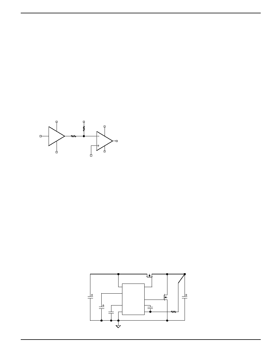
EN
150
µF/10V
Oscon
GND
V
DDQ
= 1.8V
VDDQ
V
CC
5V
1
µF
10V
120pF
MIC5162BMM
3.01K
GND
V
TT
= 0.9V@+/-7A
SUB75N03-07
220pF
SUB75N03-07
SUB75N03-07
SUB75N03-07
680
µF/4V
Oscon
VCC
EN
VREF
HSD
Comp
LSD
FB
Figure 4. DDR2 Termination
-40
-30
-20
-10
0
10
20
30
40
-7
-5
-3
-1
1
3
5
7
V
TT
- V
REF
(mV)
CURRENT (A)
MIC5162 DDR2
-7A Load Transient
TIME (200
µs/div)
V
TT
AC COUPLED
(20mV/div)
OUTPUT
CURRENT
(5A/div)
7A Load Transient
TIME (200
µs/div)
V
TT
AC COUPLED
(20mV/div)
OUTPUT
CURRENT
(5A/div)
February 2005
11
M9999-092004
MIC5162
Micrel, Inc.
Package Information
0.15 (0.006)
0.05 (0.002)
0.50 BSC (0.020)
6∞ MAX
0∞ MIN
3.15 (0.122)
2.85 (0.114)
3.10 (0.122)
2.90 (0.114)
0.30 (0.012)
0.15 (0.006)
0.26 (0.010)
0.10 (0.004)
1.10 (0.043)
0.94 (0.037)
DIMENSIONS:
MM (INCH)
0.70 (0.028)
0.40 (0.016)
4.90 BSC (0.193)
10-Pin SOP (M)
MICREL INC.
2180 FORTUNE DRIVE
SAN JOSE, CA 95131
USA
TEL
+ 1 (408) 944-0800
FAX
+ 1 (408) 474-1000
WEB
http://www.micrel.com
This information furnished by Micrel in this data sheet is believed to be accurate and reliable. However no responsibility is assumed by Micrel for its use.
Micrel reserves the right to change circuitry and specifications at any time without notification to the customer.
Micrel Products are not designed or authorized for use as components in life support appliances, devices or systems where malfunction of a product can
reasonably be expected to result in personal injury. Life support devices or systems are devices or systems that (a) are intended for surgical implant into
the body or (b) support or sustain life, and whose failure to perform can be reasonably expected to result in a significant injury to the user. A Purchaser's
use or sale of Micrel Products for use in life support appliances, devices or systems is a Purchaser's own risk and Purchaser agrees to fully indemnify
Micrel for any damages resulting from such use or sale.
© 2003 Micrel Incorporated