 | –≠–ª–µ–∫—Ç—Ä–æ–Ω–Ω—ã–π –∫–æ–º–ø–æ–Ω–µ–Ω—Ç: MIC5191 | –°–∫–∞—á–∞—Ç—å:  PDF PDF  ZIP ZIP |
April 2004
1
M9999-042804
MIC5191
Micrel
MIC5191
Ultra High-Speed, High-Current Active Filter/LDO Controller
General Description
The MIC5191 is an ultra high-speed linear regulator. It uses
an external N-Channel FET as its power device.
The MIC5191's ultra high-speed abilities can handle the fast
load demands of microprocessor cores, ASICs, and other
high-speed devices. Signal bandwidths of greater than 500kHz
can be achieved with a minimum amount of capacitance
while at the same time keeping the output voltage clean,
regardless of load demand. A powerful output driver delivers
large MOSFETs into their linear regions, achieving ultra-low
dropout voltage.
1.25V
IN
±
10% can be turned into 1V
±
1% without the use of
a large amount of capacitance.
MIC5191 (1.0V reference) is optimized for output voltages of
1.0V and higher.
The MIC5191 is offered in 10-lead 3mm
◊
3mm MLFTM and
10-lead MSOP-10 packages and has an operating junction
temperature range of ≠40
∞
C to +125
∞
C.
All support documentation can be found on Micrel's web
site at www.micrel.com.
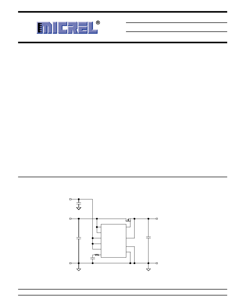
Typical Application
Features
∑ Input voltage range:
V
IN
= 1.0V to 5.5V
∑ +1.0% initial output tolerance
∑ Dropout down to 25mV@10A
∑ Filters out switching frequency noise on input
∑ Very high large signal bandwidth >500kHz
∑ PSRR >40dB at 500kHz
∑ Adjustable output voltage down to 1.0V
∑ Stable with any output capacitor
∑ Excellent line and load regulation specifications
∑ Logic controlled shutdown
∑ Current limit protection
∑ 10-lead MLFTM and MSOP-10 packages
∑ Available ≠40
∞
C to +125
∞
C junction temperature
Applications
∑ Distributed power supplies
∑ ASIC power supplies
∑ DSP,
µ
P, and
µ
C power supplies
Micrel, Inc. ∑ 1849 Fortune Drive ∑ San Jose, CA 95131 ∑ USA ∑ tel + 1 (408) 944-0800 ∑ fax + 1 (408) 474-1000 ∑ http://www.micrel.com
VIN
SGND
PGND
IS
IR3716S
OUT
VCC1
C3
0.01
µ
F
C2
10
µ
F
FB
GND
V
OUT
=1.0V@7A
GND
VCC2
EN
COMP
MIC5191
R3
12.5k
C1
0.01
µ
F
V
IN
=
1.2V
V
CC
=
12V
MicroLeadFrame and MLF are trademarks of Amkor Technology, Inc.
PowerPAK is a trademark of Siliconix, Inc.

MIC5191
Micrel
April 2004
2
M9999-042804
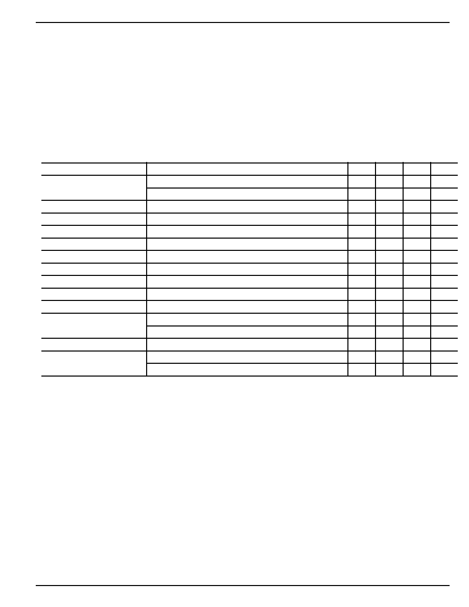
Pin Description
Pin Number
Pin Name
Pin Function
1
VIN
Input voltage (current sense +).
2
FB
Feedback input to error amplifier.
3
SGND
Signal ground.
4
VCC1
Supply to the internal voltage regulator.
5
COMP
Error amplifier output for external compensation.
6
EN
Enable (Input): CMOS-compatible.
Logic high = Enable, Logic low = Shutdown. Do not float pin.
7
VCC2
Power to output driver.
8
OUT
Output drive to gate of power MOSFET.
9
PGND
Power ground.
10
IS
Current sense.
Pin Configuration
COMP
EN
5
1
VIN
FB
SGND
VCC1
10 IS
PGND
OUT
VCC2
9
8
7
2
3
4
6
MLF-10 (ML)
Top View
Ordering Information
FB
Output
Output
Part Number
Voltage
Current
Voltage
Junction Temp. Range
Package
MIC5191BML
1V
ADJ
ADJ
≠40
∞
C to +125
∞
C
10-lead MLFTM
MIC5191BMM
1V
ADJ
ADJ
≠40
∞
C to +125
∞
C
MSOP-10
COMP
EN
6
5
1
VIN
FB
SGND
VCC1
10 IS
PGND
OUT
VCC2
9
8
7
2
3
4
MSOP-10 (MM)
Top View
April 2004
3
M9999-042804
MIC5191
Micrel
Electrical Characteristics
(6)
T
A
= 25
∞
C with V
IN
= 1.2V, V
CC
= 12V, V
OUT
= 1.0V; bold values indicate ≠40
∞
C < T
J
< +125
∞
C; unless otherwise specified.
Parameter
Condition
Min
Typ
Max
Units
Output Voltage Accuracy
At 25
∞
C
≠1
+1
%
Over temperature range
≠2
+2
%
Output Voltage Line Regulation
V
IN
= 1.2V to 5.5V
≠0.1
0.005
+0.1
%/V
Feedback Voltage
0.990
1.000
1.010
V
Output Voltage Load Regulation
I
L
= 10mA to 1A
0.02
0.5
%
VCC Pin Current (V
CC
1 + V
CC
2)
Enable = 0V
40
µ
A
VCC Pin Current
(V
CC
sig + V
CC
drv)
Enable = 5V
15
20
mA
VIN Pin Current
Current from V
IN
10
15
µ
A
FB Bias Current
13
30
µ
A
Current Limit Threshold
35
50
70
mV
Start-up Time
V
EN
= V
IN
25
100
µ
s
Enable Input Threshold
Regulator enable
0.8
0.6
V
Regulator shutdown
0.5
0.2
V
Enable Hysteresis
100
mV
Enable Pin Input Current
V
IL
< 0.2V (Regulator shutdown)
100
nA
V
IH
> 0.8V (Regulator enabled)
100
nA
Notes:
1.
Exceeding the absolute maximum ratings may damage the device.
2.
Devices are ESD sensitive. Handling precautions recommended. Human body model, 1.5k in series with 100pF.
3.
The device is not guaranteed to function outside its operating ratings.
4.
Per JESD 51-5 (1S2P Direct Attach Method).
5. Per JESD 51-3 (1S0P).
6. Specification for packaged product only.
Absolute Maximum Ratings
(1)
Supply Voltage (V
IN
) ................................................. + 6.0V
Enable Input Voltage (V
EN
) ........................................ +14V
V
CC
1, V
CC
2 .............................................................. +14V
Junction Temperature (T
J
) ................ ≠40
∞
C
T
J
+125
∞
C
ESD ......................................................................... Note 2
Operating Ratings
(3)
Supply Voltage (V
IN
) ................................. +1.0V to + 5.5V
Enable Input Voltage (V
EN
) .................................. 0V to Vcc
V
CC
1,V
CC
2 ............................................. +4.5V to +13.2V
Junction Temperature (T
J
) ................ ≠40
∞
C
T
J
+125
∞
C
Package Thermal Resistance
MLFTM
(
JA
)
(4) ..................................................................
60
∞
C/W
MSOP
(
JA
)
(5) ................................................................
200
∞
C/W

MIC5191
Micrel
April 2004
4
M9999-042804
Typical Characteristics
0.2
0.3
0.4
0.5
0.6
0.7
0.8
4
.5
5.5
6.5
7.5
8
.5
9
.5
10.5
11.5
12.5
13.5
EN
T
H
(
V
)
V
CC
Voltage (V)
Enable Threshold
vs. V
CC
Voltage
0
2
4
6
8
10
12
14
16
18
20
4
.5
5.5
6.5
7.5
8
.5
9
.5
10.5
11.5
12.5
13.5
I
nput
C
urrent
(m
A
)
VCC Voltage (V)
V
CC
Current
vs.
V
CC
Voltage
0
2
4
6
8
10
12
14
16
18
20
-40 -20 0
20 40 60 80 100 120
I
nput
C
urrent
(
µ
A
)
Temperature (
∞
C)
Input Current
vs. Temperature
9
10
11
12
13
14
15
4
.5
5.5
6.5
7.5
8
.5
9
.5
10.5
11.5
12.5
13.5
F
eedbac
k C
urrent
(
µ
A
)
V
CC
Voltage(V)
Feedback Current
vs. V
CC
Voltage
0
5
10
15
20
25
-40 -20 0
20 40 60 80 100 120
F
eedbac
k C
urrent
(
µ
A
)
Temperature (
∞
C)
Feedback Current
vs. Temperature
0.995
0.996
0.997
0.998
0.999
1
1.001
1.002
1.003
1.004
1.005
0
1
2
3
4
5
6
7
8
9 10
O
utput
V
oltage
(
V
)
Output Current (A)
Load Regulation
0.995
0.996
0.997
0.998
0.999
1
1.001
1.002
1.003
1.004
1.005
-40 -20 0
20 40 60 80 100 120
V
out
(
V
)
Temp (C)
V
OUT
vs. Temperature
0.995
0.996
0.997
0.998
0.999
1
1.001
1.002
1.003
1.004
1.005
4
.5
5.5
6.5
7.5
8
.5
9
.5
10.5
11.5
12.5
V
out
(
V
)
Vcc (V)
V
OUT
vs. Vcc Voltage
40
45
50
55
60
65
4
.5
5.5
6.5
7.5
8
.5
9
.5
10.5
11.5
12.5
13.5
CURRENT
L
IMIT
(m
A
)
V
CC
(V)
Current Limit Threshold
vs. V
cc
Voltage
0
5
10
15
20
25
30
35
40
45
50
4
.5
5.5
6.5
7.5
8
.5
9
.5
10.5
11.5
12.5
13.5
E
nable
T
ime
(
µ
sec)
V
CC
(V) Voltage
Enable Time
vs. V
CC
Voltage
April 2004
5
M9999-042804
MIC5191
Micrel
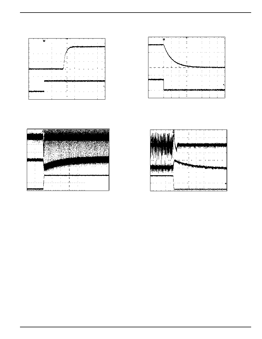
Disable Transient
TIME (100
µ
s/div)
OUTPUT
(
500
m
V
/div)
ENAB
L
E
(
1V
/div)
Functional Characteristics
TIME (100
µ
s/div)
OUTPUT
(
10
m
V
/div)
L
OAD CURRENT
(
5A
/div)
INPUT
(
100
m
V
/div)
10A Load Transient
Enable Transient
TIME (10
µ
s/div)
OUTPUT
(
500
m
V
/div)
ENAB
L
E
(
1V
/div)
TIME (100
µ
s/div)
INPUT
(
100
m
V
/div)
OUTPUT
(
10
m
V
/div)
L
OAD CURRENT
(
5A
/div)
Transient Response

MIC5191
Micrel
April 2004
6
M9999-042804
Functional Diagram
Figure 1. MIC5191 Block Diagram
Functional Description
VIN
The VIN pin is connected to the N-Channel drain. VIN is the
input power being supplied to the output. This pin is also used
to power the internal current limit comparator and compare
the ISENSE voltage for current limit. The voltage range is
from 1.0V min to 5.5V max.
ISENSE
The ISENSE pin is the other input to the current limit com-
parator. The output current is limited when the ISENSE pin's
voltage is 50mV less than the VIN pin. In cases where there
is a current limited source and there isn't a need for current
limit, this pin can be tied directly to VIN. Its operating voltage
range, like the VIN pin, is 1.0V min to 5.5V max.
VCC1, VCC2
VCC1 supplies the error amplifier and internal reference,
while VCC2 supplies the output gate drive. For this reason,
ensure these pins have good input capacitor bypassing for
better performance. The operating range is from 4.5V to
13.2V and both VCC pins should be tied together. Ensure that
the voltage supplied is greater than a gate-source threshold
above the output voltage for the N-Channel MOSFET se-
lected.
Output
The output drives the external N-Channel MOSFET and is
powered from V
CC
. The output can sink and source over
150mA of current to drive either an N-Channel MOSFET or an
external NPN transistor. The output drive also has short-
circuit current protection.
Enable
The MIC5191 comes with an active-high enable pin that
allows the regulator to be disabled. Forcing the enable pin low
disables the regulator and sends it into a low off-mode-
current state. Forcing the enable pin high enables the output
voltage. The enable pin cannot be left floating; a floating
enable pin may cause an indeterminate state on the output.
FB
The feedback pin is used to sense the output voltage for
regulation. The feedback pin is compared to an internal 1.0V
reference and the output adjusts the gate voltage accordingly
to maintain regulation. Since the feedback biasing current is
typically 13
µ
A, smaller feedback resistors should be used to
minimize output voltage error.
COMP
COMP is the external compensation pin. This allows com-
plete control over the loop to allow stability for any type of
output capacitor, load currents and output voltage. A detailed
explanation of how to compensate the MIC5191 is in the
"Designing with the MIC5191" section.
SGND, PGND
SGND is the internal signal ground which provides an iso-
lated ground path from the high current output driver. The
signal ground provides the grounding for noise sensitive
circuits such as the current limit comparator, error amplifier
and the internal reference voltage.
PGND is the power ground and is the grounding path for the
output driver.
OUTPUT
CONTROL
AND
LEVEL
SHIFT
CURRENT LIMIT
AMPLIFIER
ERROR
AMPLIFIER
ENABLE
VIN
IS
VCC2
OUT
PGND
FB
1V
50mV
SGND
EN
VCC1
COMP
INTERNAL
VOLTAGE
REGULATOR
April 2004
7
M9999-042804
MIC5191
Micrel
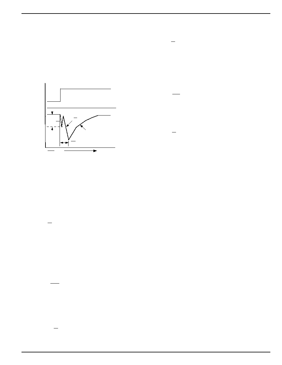
Applications Information
Designing with the MIC5191
Anatomy of a transient response
A voltage regulator can maintain a set output voltage while its
exterior world is pushing and pulling in its demand for power.
The measure of a regulator is generally how accurately and
effectively it can maintain that voltage, regardless of how the
load demands power. One measure of regulator response is
the load step. This is an intuitive look at how the regulator
responds to a change in load current. Figure 2 is a look at the
transient response to a load step.
Figure 2. Typical Transient Response
At the start of a circuit's power demand, the output voltage is
regulated to its set point, while the load current runs at a
constant rate. For many different reasons, a load may ask for
more current without warning. When this happens, the regu-
lator needs some time to determine the output voltage drop.
This is determined by the speed of the control loop. So, until
enough time has elapsed, the control loop is oblivious to the
voltage change. The output capacitor must bear the burden
of maintaining the output voltage.
V
L
di
dt
=
Since this is a sudden change in voltage, the capacitor will try
to maintain voltage by discharging current to the output. The
first voltage drop is due to the output capacitor's ESL (equiva-
lent series inductance). The ESL will resist a sudden change
in current from the capacitor and drop the voltage quickly. The
amount of voltage drop during this time will be proportional to
the output capacitor's ESL and the speed at which the load
steps. Slower load current transients will reduce this effect.
V
L
di
dt
=
Placing multiple small capacitors with low ESL in parallel can
help reduce the total ESL and reduce voltage droop during
high speed transients. For high speed transients, the greatest
voltage deviation will generally be caused by output capacitor
ESL and parasitic inductance.
V
L
di
dt
=
After the current has overcome the effects of the ESL, the
output voltage will begin to drop proportionally to time and
inversely proportional to output capacitance.
The relationship to output voltage variation will depend on two
aspects, loop bandwidth and output capacitance. The output
capacitance will determine how far the voltage will fall over a
given time. With more capacitance, the drop in voltage will fall
at a decreased rate. This is the reason that for the same
bandwidth, more capacitance provides a better transien-
response
Also, the time it takes for the regulator to respond is directl
proportional to its gain bandwidth. Higher bandwidth contro
loops respond quicker causing a reduced droop on the suppl
for the same amount of capacitance
Final recovery back to the regulated voltage is the final phas
of transient response and the most important factors are gai
and time. Higher gain at higher frequency will get the outpu
voltage closer to its regulation point quicker. The final settlin
point will be determined by the load regulation, which i
proportional to DC (0Hz) gain and the associated loss terms
There are other factors that contribute to large signal tran-
sient response, such as source impedance, phase margin
and PSRR. For example, if the input voltage drops due t
source impedance during a load transient, this will contribut
to the output voltage deviation by filtering through to th
output reduced by the loops PSRR at the frequency of th
voltage transient. It is straightforward: good input capaci-
tance reduces the source impedance at high frequencies
Having between 35
∞
and 45
∞
of phase margin will help spee
up the recovery time. This is caused by the initial overshoo
in response to the loop sensing a low voltage
Compensatio
The MIC5191 allows the flexibility of externally controlling th
gain and bandwidth. This allows the MIC5191 design to b
tailored to each individual design
In designing the MIC5191, it is important to maintain ad-
equate phase margin. This is generally achieved by havin
the gain cross the 0dB point with a single pole 20dB/decad
roll-off. The compensation pin is configured as Figure
demonstrates
Figure 3. Internal Compensatio
V
C
idt
=
1
V
C
idt
=
1
V
C
idt
=
1
Time
idt
C
V =
1
BW
1
Load
C
urrent
O
utput
V
oltage
AC
-
C
oupled
Output voltage vs. time
during recovery is
directly proportional to
gain vs. frequency.
V
=
L
di
dt
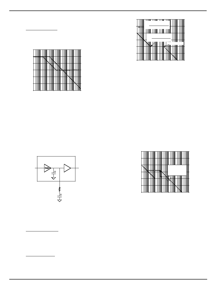
MIC5191
Micrel
April 2004
8
M9999-042804
This places a pole at 2.3kHz at 80dB and calculates as
follows.
F
M
pF
F
kHz
P
P
=
◊
◊
=
1
2
3 42
20
2 32
.
.
-20
0
20
40
60
80
100
0.01
0.1
1
10
100
1000
10000 100000
Frequency (KHz)
G
a
in
(
d
B
)
-45
0
45
90
135
180
225
P
h
ase (
D
eg
)
Figure 4. Internal Compensation
Frequency Response
There is single pole roll off. For most applications, an output
capacitor is required. The output capacitor and load resis-
tance create another pole. This causes a two-pole system
and can potentially cause design instability with inadequate
phase margin. What should we do? Answer: we compensate
it externally. By providing a dominant pole and zero≠allowing
the output capacitor and load to provide the final pole≠a net
single pole roll off is created, with the zero canceling the
dominant pole. Figure 5 demonstrates:
Error Amplifier
Driver
3.42M
20pF
Internal
External
Comp
R
COMP
C
COMP
Figure 5. External Compensation
Placing an external capacitor (C
COMP
) and resistor (R
COMP
)
for the external pole-zero combination. Where the dominant
pole can be calculated as follows:
F
M
C
P
COMP
=
◊
◊
1
2
3 42
.
And the zero can be calculated as follows:
F
R
C
Z
COMP
COMP
=
◊
◊
1
2
This allows for high DC gain, and high bandwidth with the
output capacitor and the load providing the final pole.
Figure 6. External Compensation
Frequency Response
It is recommended that the gain bandwidth should be de-
signed to be less than 1 MHz. This is because most capaci-
tors lose capacitance at high frequency and becoming resis-
tive or inductive. This can be difficult to compensate for and
can create high frequency ringing or worse, oscillations.
By increasing the amount of output capacitance, transient
response can be improved in multiple ways. First, the rate of
voltage drop vs. time is decreased. Also, by increasing the
output capacitor, the pole formed by the load and the output
capacitor decreases in frequency. This allows for the increas-
ing of the compensation resistor, creating a higher mid-band
gain.
Figure 7. Increasing Output Capacitance
This will have the effect of both decreasing the voltage drop
as well as returning closer and faster to the regulated voltage
during the recovery time.
MOSFET Selection
The typical pass element for the MIC5191 is an N-Channel
MOSFET. There are multiple considerations when choosing
a MOSFET. These include:
∑ V
IN
to V
OUT
differential
∑ Output Current
∑ Case Size/Thermal Characteristics
∑ Gate Capacitance (C
ISS
<10nF)
∑ Gate to Source threshold
-20
0
20
40
60
80
100
0.01
0.1
1
10
100
1000
10000 100000
Frequency (KHz)
Ga
i
n
(
d
B
)
-45
0
45
90
135
180
225
P
h
ase
(
D
eg
)
The Dominant Pole
External Zero
R
LOAD
◊
C
OUT
Pole
Ccomp
M
Fp
◊
◊
=
42
.
3
2
1
Ccomp
Rcomp
Fz
◊
◊
=
2
1
-20
0
20
40
60
80
100
0.01
0.1
1
10
100
1000
10000 100000
Frequency (KHz)
Ga
i
n
(
d
B
)
-45
0
45
90
135
180
225
P
h
ase
(
D
eg
)
Increasing C
OUT
reduces
the load resistance and
output capacitor pole
allowing for an increase
in mid-band gain.

April 2004
9
M9999-042804
MIC5191
Micrel
The V
IN
(min) to V
OUT
ratio and current will determine the
maximum R
DSON
required. For example, for a 1.8V (
±
5%) to
1.5V conversion at 5A of load current, dropout voltage can be
calculated as follows (using V
IN
(min):
R
V
V
I
R
1 71V 1 5V
5A
R
m
DSON
IN
OUT
OUT
DSON
DSON
=
-
(
)
=
-
(
)
=
.
.
42
For performance reasons, we do not want to run the N-
Channel in dropout. This will seriously affect transient re-
sponse and PSRR (power supply ripple rejection). For this
reason, we want to select a MOSFET that has lower than
42m
for our example application.
Size is another important consideration. Most importantly,
the design must be able to handle the amount of power being
dissipated.
The amount of power dissipated can be calculated as follows
(using V
IN
(max)):
P
D
= (V
IN
≠ V
OUT
)
◊
I
OUT
P
D
= (1.89V ≠ 1.5V)
◊
5A
P
D
= 1.95W
Now that we know the amount of power we will be
dissipating, we will need to know the maximum ambient air
temperature. For our case we're going to assume a
maximum of 65
∞
C ambient temperature, though different
MOSFETs have different maximum operating junction
temperatures. Most MOSFETs are rated to 150
∞
C, while
others are rated as high as 175
∞
C. In this case, we're
going to limit our maximum junction temperature to 125
∞
C.
The MIC5191 has no internal thermal protection for the
MOSFET so it is important that the design provides margin
for the maximum junction temperature. Our design will
maintain better than 125
∞
C junction temperature with
1.95W of power dissipation at an ambient temperature of
65
∞
C. Our thermal resistance calculates as follows:
JA
J
J
D
JA
JA
T max
T ambient
P
125 C
65 C
1.95W
C W
=
( )
-
(
)
=
∞ - ∞
=
∞
31
/
So our package must have a thermal resistance less than
31
∞
C /W. Table 1 shows a good approximation of power
dissipation and package recommendation.
Package Power Dissipation
TSOP-6
<850mW
TSSOP-8
<950mW
TSSOP-8
<1W
PowerPAKTM 1212-8
<1.1W
SO-8
<1.125W
PowerPAKTMSO-8 D-Pack
<1.4W
TO-220/TO-263 (D
2
pack)
>1.4W
Table 1. Power Dissipation and
Package Recommendation
In our example, our power dissipation is greater than
1.4W, so we'll choose a TO-263 (D
2
Pack) N-Channel
MOSFET.
JA
is calculated as follows.
JA
=
JC
+
CS
+
SA
Where
JC
is the junction to case resistance,
CS
is the
case-to-sink resistance and the
SA
is the sink-to-ambi-
ent air resistance.
In the D
2
package we've selected, the
JC
is 2
∞
C/W. The
CS
, assuming we are using the PCB as the heat sink,
can be approximated to 0.2
∞
C/W. This allows us to
calculate the minimum
SA
:
SA
=
JA
≠
CS
≠
JC
SA
= 31
∞
C/W ≠ 0.2
∞
C/W ≠ 2
∞
C/W
SA
= 28.8
∞
C/W
Referring to
Application Hint 17, Designing PCB Heat
Sinks
, the minimum amount of copper area for a D
2
pack
at 28.8
∞
C/W is 2750mm
2
(or 0.426in
2
). The solid line
denotes convection heating only (2 oz. copper) and the
dotted line shows thermal resistance with 250LFM air-
flow. The copper area can be significantly reduced by
increasing airflow or by adding external heat sinks.
Figure 8. PC Board Heat Sink
Another important characteristic is the amount of gate
capacitance. Large gate capacitance can reduce tran-
sient performance by reducing the ability of the MIC5190
to slew the gate. It is recommended that the MOSFET
used has an input capacitance <10nF (C
ISS
).
PC Board Heat Sink
Thermal Resistance vs. Area

MIC5191
Micrel
April 2004
10
M9999-042804
ource threshold specified in most MOSFET data sheets
refers to the minimumvoltage needed to fully enhance the
MOSFET. Although for the most part, the MOSFET will be
operating in the linear region and the V
GS
(gate-source
voltage) will be less than the fully enhanced V
GS
, it is
recommended the V
CC
voltage has 2V over the minimum
V
GS
and output voltage. This is due to the saturation
voltage of the MIC5191 output driver.
V
CC1,2
2V + V
GS
+ V
OUT
For our example, with a 1.5V output voltage, our MOSFET is
fully enhanced at 4.5V
GS
, our V
CC
voltage should be greater
or equal to 8V.
Input Capacitor
Good input bypassing is important for improved perfor-
mance. Low ESR and low ESL input capacitors reduce both
the drain of the N-Channel MOSFET, as well as the source
impedance to the MIC5191. When a load transient on the
output occurs, the load step will also appear on the input.
Deviations on the input voltage will be reduced by the
MIC5191's PSRR, but nonetheless appear on the output.
There is no minimum input capacitance, but for optimal
performance it is recommended that the input capacitance be
equal to or greater than the output capacitance.
Output Capacitor
The MIC5191 is stable with any type or value of output
capacitor (even without any output capacitor!). This allows
the output capacitor to select which parameters of the regu-
lator are important. In cases where transient response is the
most important, low ESR and low ESL ceramic capacitors are
recommended. Also, the more capacitance on the output, the
better the transient response.
Figure 9. Post Regulator
4
5
3
1
2
VIN
EN/UVLO
CSH
VOUT
FB
LSD
560pF
8.06k
BST
COMP
6
HSD
12
VSW
11
GND
D1
SD103BWS
2.2
µ
F
10V
0.1
µ
F
10
8
VDD
7
U1 MIC2198-BML
9
100pF
11.5k
100k
V
OUT
V
OUT
CSH
J2
EN
J1
+V
IN
V
IN
CSH
V
OUT
10k
10k
10
10
1
µ
F
25V
330
µ
F
16V
10
µ
F
10
µ
F
10
µ
F
10
µ
F
10
µ
F
22
µ
F
1V
OUT
@10A
D2
1N5819HW
IRF7821
IRF7821
L1
1.8
µ
H
CDEP134-1R8MC-H
12.4k
330
µ
F
Tantalum
OUT
VCC1
VCC2
VIN
FB
ISENSE
COMP
GND
10nF
100
10
MIC5191
1
µ
F
V
OUT
12V
April 2004
11
M9999-042804
MIC5191
Micrel
Feedback Resistors
IR3716S
R1
COUT
R2
FB
GND
MIC5191
V
OUT
Figure 10. Adjustable Output
The feedback resistors adjust the output to the desired
voltage and can be calculated as follows:
V
V
R1
R2
OUT
REF
=
+
1
V
REF
is equal to 1.0V for the MIC5191. The minimum output
voltage (R1=0) is 0.5V. For output voltages less than 1V, use
the MIC5190.
The resistor tolerance adds error to the output voltage. These
errors are accumulative for both R1 and R2. For example, our
resistors selected have a
±
1% tolerance. This will contribute
to a
±
2% additional error on the output voltage.
The feedback resistors must also be small enough to allow
enough current to the feedback node. Large feedback resis-
tors will contribute to output voltage error.
V
R1 I
V
1k
1
A
V
mV
ERROR
FB
ERROR
ERROR
=
◊
=
◊ µ
=
2
12
For our example application, this will cause an increase in
output voltage of 12mV. For the percentage increase,
V
V
V
V
12mV
1.5V
V
ERROR
ERROR
OUT
ERROR
ERROR
%
%
%
. %
=
◊
=
◊
=
100
100
0 8
By reducing R1 to 100
, the error contribution by the feed-
back resistors and feedback current is reduced to less than
0.1%. This is the reason R1 should not be greater than 100
.
Applying the MIC5191
Linear Regulator
The primary purpose of the MIC5191 is as a linear regulator,
which enables an input supply voltage to drop down through
the resistance of the pass element to a regulated output
voltage.
Active Filter
Another application for the MIC5191 is as an active filter on
the output of a switching regulator. This improves the power
supply in several ways.
First, using the MIC5191 as a filter on the output can signifi-
cantly reduce high frequency noise. Switching power sup-
plies tends to create noise at the switching frequency in the
form of a triangular voltage ripple. High frequency noise is
also created by the high-speed switching transitions. A lot of
time, effort, and money are thrown into the design of switch-
ing regulators to minimize these effects as much as possible.
Figure 9 shows the MIC5191 as a post regulator.
TIME (1µs/div)
INPUT
RIPP
L
E
(
100
m
V
/div)
OUTPUT
(
10
m
V
/div)
V
OUT
= 1V
I
LOAD
= 10A
Figure 11. Ripple Reduction
Figure 11 shows the amount of ripple reduction for a 500 KHz
switching regulator. The fundamental switching frequency is
reduced from greater than 100mV to less than 10mV.
Figure 12. 10A Load Transient
The transient response also contributes to the overall AC
output voltage deviation. Figure 12 shows a 1A to 10A load
transient. The top trace is the output of the switching regulator
(same circuit as Figure10). The output voltage undershoots
by 100mV. Just by their topology, linear regulators have the
ability to respond at much higher speeds than a switching
regulator. Linear regulators do not have the limitation or
restrictions of switching regulators which must reduce their
bandwidth to less than their switching frequency.
TIME (100
µ
s/div)
OUTPUT
(
10
m
V
/div)
L
OAD CURRENT
(
5A
/div)
INPUT
(
100
m
V
/div)

MIC5191
Micrel
April 2004
12
M9999-042804
Using the MIC5191 as a filter for a switching regulator
reduces output noise due to ripple and high frequency switch-
ing noise. It also reduces undershoot (Figure 12) and over-
shoot (Figure 13) due to load transients with decreased
capacitance.
Figure 13. Transient Response
Due to the high DC gain (80dB) of the MIC5191, it also adds
increased output accuracy and extremely high load regula-
tion.
Distributed Power Supply
As technology advances and processes move to smaller and
smaller geometries, voltage requirements go down and cur-
rent requirements go up. This creates unique challenges
when trying to supply power to multiple devices on a board.
When there is one load to power, the difficulties are not quite
as complex; trying to distribute power to multiple loads from
one supply is much more problematic.
If a large circuit board has multiple small-geometry ASICs, it
will require the powering of multiple loads with its one power
source. Assuming that the ASICs are dispersed throughout
the board and that the core voltage requires a regulated 1V,
Figure 14 shows the long traces from the power supply to the
loads. Not only do we have to contend with the tolerance of
the supply (line regulation, load regulation, output accuracy
and temperature tolerances), but the trace lengths create
additional issues with resistance and inductance. With lower
voltages these parasitic values can easily bump the output
voltage out of a usable tolerance.
Load
Load
Switching
Power
Supply
Circuit Board
Load
Load
Long Traces
Figure 14. Board Layout
But by placing multiple, small MIC5191 circuits close to each
load, the parasitic trace elements caused by distance to the
power supply are almost completely negated. By adjusting
the switching supply voltage to 1.2V, for example, the MIC5191
will provide accurate 1V output, efficently and with very little
noise.
Figure 15. Improved Distributed Supplies
Load
Load
Switching
Power
Supply
Circuit Board
Load
Load
MIC5191
MIC5191
MIC5191
MIC5191
TIME (100
µ
s/div)
INPUT
(
100
m
V
/div)
OUTPUT
(
10
m
V
/div)
L
OAD CURRENT
(
5A
/div)
April 2004
13
M9999-042804
MIC5191
Micrel
Package Information
0.15 (0.006)
0.05 (0.002)
0.50 BSC (0.020)
6
∞
MAX
0
∞
MIN
3.15 (0.122)
2.85 (0.114)
3.10 (0.122)
2.90 (0.114)
0.30 (0.012)
0.15 (0.006)
0.26 (0.010)
0.10 (0.004)
1.10 (0.043)
0.94 (0.037)
DIMENSIONS:
MM (INCH)
0.70 (0.028)
0.40 (0.016)
4.90 BSC (0.193)
10-Pin MSOP (MM)
MICREL, INC.
1849 FORTUNE DRIVE
SAN JOSE, CA 95131
USA
TEL
+ 1 (408) 944-0800
FAX
+ 1 (408) 474-1000
WEB
http://www.micrel.com
The information furnished by Micrel in this data sheet is believed to be accurate and reliable. However, no responsibility is assumed by Micrel for its use.
Micrel reserves the right to change circuitry and specifications at any time without notification to the customer.
Micrel Products are not designed or authorized for use as components in life support appliances, devices or systems where malfunction of a product can
reasonably be expected to result in personal injury. Life support devices or systems are devices or systems that (a) are intended for surgical implant into
the body or (b) support or sustain life, and whose failure to perform can be reasonably expected to result in a significant injury to the user. A Purchaser's
use or sale of Micrel Products for use in life support appliances, devices or systems is at Purchaser's own risk and Purchaser agrees to fully indemnify
Micrel for any damages resulting from such use or sale.
© 2004 Micrel, Incorporated.
10-Lead MLFTM (ML)