
MIC5202
Micrel
July 1998
1
MIC5202
MIC5202
Dual 100mA Low-Dropout Regulator
Final Information
Typical Application
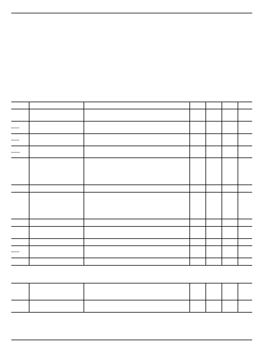
Ordering Information
Part Number
Volts Accuracy Temperature Range* Package
MIC5202-3.0BM
3.0
1%
≠40
∞
C to +125
∞
C
SO-8
MIC5202-3.3BM
3.3
1%
≠40
∞
C to +125
∞
C
SO-8
MIC5202-4.8BM
4.85
1%
≠40
∞
C to +125
∞
C
SO-8
MIC5202-5.0BM
5.0
1%
≠40
∞
C to +125
∞
C
SO-8
Pin Configuration
Other voltages are available; contact Micrel for details.
Features
∑
High output voltage accuracy
∑
Variety of output voltages
∑
Guaranteed 100mA output
∑
Low quiescent current
∑
Low dropout voltage
∑
Extremely tight load and line regulation
∑
Very low temperature coefficient
∑
Current and thermal limiting
∑
Reverse-battery protection
∑
Zero OFF mode current
∑
Logic-controlled electronic shutdown
∑
Available in SO-8 package
Applications
∑
Cellular Telephones
∑
Laptop, Notebook, and Palmtop Computers
∑
Battery Powered Equipment
∑
PCMCIA V
CC
and V
PP
Regulation/Switching
∑
Bar Code Scanners
∑
SMPS Post-Regulator/ DC to DC Modules
∑
High Efficiency Linear Power Supplies
General Description
The MIC5202 is a family of dual linear voltage regulators with
very low dropout voltage (typically 17mV at light loads and
210mV at 100mA), and very low ground current (1mA at
100mA output≠each section), offering better than 1% initial
accuracy with a logic compatible ON/OFF switching input.
Designed especially for hand-held battery powered devices,
the MIC5202 is switched by a CMOS or TTL compatible logic
signal. This ENABLE control my be tied directly to V
IN
if
unneeded. When disabled, power consumption drops nearly
to zero. The ground current of the MIC5202 increases only
slightly in dropout, further prolonging battery life. Key MIC5202
features include protection against reversed battery, current
limiting, and over-temperature shutdown.
The MIC5202 is available in several fixed voltages. Other
options are available; contact Micrel for details.
MIC5202-3.3
Enable B
Output A
Output B
Enable A
Both GROUND pins must be tied to
the same potential. V
IN
(A) and V
IN
(B) may run
from separate supplies.
* Junction Temperature
1
µ
(x2)
ENABLE pins may be tied directly to V
IN
GROUND
VOUT (A)
VIN (A)
ENABLE (B)
MIC5202-xxBM
VOUT (B)
ENABLE (A)
VIN (B)
GROUND
Micrel, Inc. ∑ 1849 Fortune Drive ∑ San Jose, CA 95131 ∑ USA ∑ tel + 1 (408) 944-0800 ∑ fax + 1 (408) 944-0970 ∑ http://www.micrel.com
MIC5202
Micrel
MIC5202
2
July 1998
Electrical Characteristics
Limits in standard typeface are for T
J
= 25
∞
C and limits in boldface apply over the junction temperature range of ≠40
∞
C to +125
∞
C.
Specifications are for each half of the (dual) MIC5202. Unless otherwise specified, V
IN
= V
OUT
+ 1V, I
L
= 1mA, C
L
= 10
µ
F, and V
CONTROL
2.0V.
Symbol
Parameter
Condition
Min
Typ
Max
Units
V
O
Output Voltage
Variation from specified V
OUT
≠1
1
%
Accuracy
≠2
2
V
O
Output Voltage
(Note 2)
40
150
ppm/
∞
C
T
Temperature Coef.
V
O
Line Regulation
V
IN
= V
OUT
+ 1 V to 26V
0.004
0.10
%
V
O
0.40
V
O
Load Regulation
I
L
= 0.1mA to 100mA (Note 3)
0.04
0.16
%
V
O
0.30
V
IN
≠ V
O
Dropout Voltage
I
L
= 100
µ
A
17
mV
(Note 4)
I
L
= 20mA
130
I
L
= 30mA
150
I
L
= 50mA
180
I
L
= 100mA
225
350
I
Q
Quiescent Current
V
CONTROL
0.7V (Shutdown)
0.01
µ
A
I
GND
Ground Pin Current
V
CONTROL
2.0V, I
L
= 100
µ
A
170
µ
A
I
L
= 20mA
270
I
L
= 30mA
330
I
L
= 50mA
500
I
L
= 100mA
1200
1500
PSRR
Ripple Rejection
75
dB
I
GNDDO
Ground Pin
V
IN
= 0.5V less specified V
OUT
, I
L
= 100
µ
A
270
330
µ
A
Current at Dropout
(Note 5)
I
LIMIT
Current Limit
V
OUT
= 0V
280
mA
V
O
Thermal Regulation
(Note 6)
0.05
%/W
P
D
e
n
Output Noise
100
µ
V
Control Input
Input Voltage Level
V
IL
Logic Low
OFF
0.7
V
Logic High
ON
2.0
I
IL
Control Input Current
V
IL
0.7V
0.01
µ
A
IH
V
IH
2.0V
8
50
Absolute Maximum Ratings
Absolute Maximum Ratings indicate limits beyond which damage
to the device may occur. Electrical specifications do not apply when
operating the device beyond its specified Operating Ratings.
Power Dissipation ............................................... Internally Limited
Lead Temperature (Soldering, 5 seconds) .......................... 260
∞
C
Operating Junction Temperature Range ............. ≠40
∞
C to +125
∞
C
Input Supply Voltage ................................................ ≠20V to +60V
ENABLE Input Voltage ............................................. ≠20V to +60V
SO-8
JA
....................................................................... See Note 1
Recommended Operating Conditions
Input Voltage ............................................................... 2.5V to 26V
Operating Junction Temperature Range ............. ≠40
∞
C to +125
∞
C
ENABLE Input Voltage ..................................................... 0V to V
IN
MIC5202
Micrel
July 1998
3
MIC5202
Note 1:
Absolute maximum ratings indicate limits beyond which damage to the component may occur. Electrical specifications do not
apply when operating the device outside of its rated operating conditions. The maximum allowable power dissipation is a
function of the maximum junction temperature, T
J(MAX)
the junction-to-ambient thermal resistance,
JA
, and the ambient
temperature, T
A
. The maximum allowable power dissipation at any ambient temperature is calculated using: P
(MAX)
=
(T
J(MAX)
≠ T
A
) /
JA.
Exceeding the maximum allowable power dissipation will result in excessive die temperature, and the
regulator will go into thermal shutdown. The junction to ambient thermal resistance of the MIC5202BM is 160
∞
C/W mounted
on a PC board.
Note 2:
Output voltage temperature coefficient is defined as the worst case voltage change divided by the total temperature range.
Note 3:
Regulation is measured at constant junction temperature using low duty cycle pulse testing. Parts are tested for load regulation
in the load range from 0.1mA to 100mA. Changes in output voltage due to heating effects are covered by the thermal regulation
specification.
Note 4:
Dropout Voltage is defined as the input to output differential at which the output voltage drops 2% below its nominal value
measured at 1V differential.
Note 5:
Ground pin current is the regulator quiescent current plus pass transistor base current. The total current drawn from the supply
is the sum of the load current plus the ground pin current.
Note 6:
Thermal regulation is defined as the change in output voltage at a time t after a change in power dissipation is applied, excluding
load or line regulation effects. Specifications are for a 100mA load pulse at V
IN
= 26V for t = 10ms, and is measured separately
for each section.
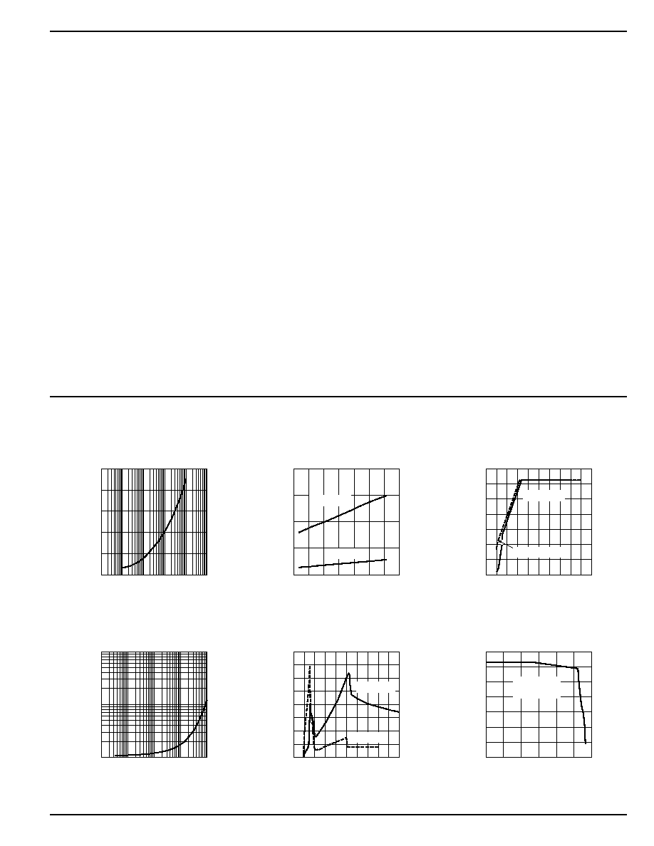
0
50
100
150
200
250
0.01
0.1
1
10
100
1000
DROPOUT VOLTAGE (mV)
OUTPUT CURRENT (mA)
Dropout Voltage
vs. Output Current
0.0
0.1
0.2
0.3
0.4
-60 -30
0
30
60
90 120 150
DROPOUT VOLTAGE (V)
TEMPERATURE (
∞
C)
Dropout Voltage
vs. Temperature
I
L
= 100mA
I
L
= 1mA
0.0
0.5
1.0
1.5
2.0
2.5
3.0
3.5
0
2
4
6
8
10
OUTPUT VOLTAGE (V)
INPUT VOLTAGE (V)
Dropout
Characteristics
I
L
= 100mA
I
L
= 100
µ
A, 1mA
0.1
1
10
0.01
0.1
1
10
100
GROUND CURRENT (mA)
OUTPUT CURRENT (mA)
Ground Current
vs. Output Current
0.0
0.2
0.4
0.6
0.8
1.0
1.2
1.4
1.6
0
2
4
6
8
10
GROUND CURRENT (mA)
SUPPLY VOLTAGE (V)
Ground Current
vs. Supply Voltage
I
L
= 100mA
I
L
= 1mA
0.0
0.5
1.0
1.5
2.0
2.5
3.0
3.5
0.0
0.1
0.2
0.3
OUTPUT VOLTAGE (V)
OUTPUT CURRENT (A)
Output Voltage
vs. Output Current
C
IN
= 2.2
µ
F
C
OUT
= 4.7
µ
F
Typical Characteristics
(Each Regulator--2 Regulators/Package)

MIC5202
Micrel
MIC5202
4
July 1998
0.15
0.20
0.25
0.30
-60 -30
0
30
60
90 120 150
GROUND CURRENT (mA)
TEMPERATURE (
∞
C)
Ground Current
vs. Temperature
I
LOAD
= 100
µ
A
C
IN
= 2.2
µ
F
C
OUT
= 4.7
µ
F
1.0
1.1
1.2
1.3
1.4
1.5
-50
0
50
100
150
GROUND CURRENT (mA)
TEMPERATURE (
∞
C)
Ground Current
vs. Temperature
I
LOAD
= 100mA
C
IN
= 2.2
µ
F
C
OUT
= 4.7
µ
F
-100
0
100
200
-5
0
5
10 15 20 25 30 35
LOAD (mA)
TIME (ms)
Thermal Regulation
(3.3V Version)
-50
0
50
100
OUTPUT (mV)
C
L
= 4.7
µ
F
3.0
3.1
3.2
3.3
3.4
3.5
3.6
-60 -30
0
30
60
90 120 150
OUTPUT VOLTAGE (V)
TEMPERATURE (
∞
C)
Output Voltage vs. Temp.
(3.3V Version)
C
IN
= 2.2
µ
F
C
OUT
= 4.7
µ
F
3 DEVICES:
HI / AVG / LO
CURVES APPLICABLE
AT 100
µ
A AND 100mA
100
120
140
160
180
200
220
240
260
280
300
-60 -30
0
30
60
90 120 150
OUTPUT CURRENT (mA)
TEMPERATURE (
∞
C)
Output Current
vs. Temperature
V
OUT
= 0V
(SHORT CIRCUIT)
V
OUT
= 3.3V
3.20
3.21
3.22
3.23
3.24
3.25
3.26
3.27
3.28
3.29
3.30
-60 -30
0
30
60
90 120 150
MIN. INPUT VOLTAGE (V)
TEMPERATURE (
∞
C)
Minimum Input Voltage
vs. Temperature
C
IN
= 2.2
µ
F
C
OUT
= 4.7
µ
F
I
LOAD
= 1mA
0
50
100
150
200
250
300
1
2
3
4
5
6
7
SHORT CIRCUIT CURRENT (mA)
INPUT VOLTAGE (V)
Short Circuit Current
vs. Input Voltage
C
IN
= 2.2
µ
F
C
OUT
= 4.7
µ
F
V
OUT
= 3.3V
-30
-20
-10
0
10
20
OUTPUT (mV)
0
100
200
300
-2
0
2
4
6
8
10
OUTPUT (mA)
TIME (ms)
Load Transient
C
L
= 4.7
µ
F
0
100
200
300
-10
0
10
20
30
40
OUTPUT (mA)
TIME (ms)
Load Transient
-30
-20
-10
0
10
20
OUTPUT (mV)
C
L
= 47
µ
F
0
20
40
60
80
100
120
0
1
2
3
4
5
6
7
8
9 10
SUPPLY CURRENT (mA)
SUPPLY VOLTAGE (V)
Supply Current vs. Supply
Voltage (3.3V Version)
R
L
= 33
-10
-5
0
5
10
OUTPUT (mV)
2
4
6
8
-0.2
0
0.2
0.4
0.6
0.8
INPUT (V)
TIME (ms)
Line Transient
C
L
= 1
µ
F
I
L
= 1mA
-5
0
5
10
15
OUTPUT (mV)
2
4
6
8
-0.1
0
0.1 0.2 0.3 0.4 0.5 0.6
INPUT (V)
TIME (ms)
Line Transient
C
L
= 10
µ
F
I
L
= 1mA

MIC5202
Micrel
July 1998
5
MIC5202
0
10
20
30
40
50
60
0
1
2
3
4
5
6
7
SUPPLY CURRENT (mA)
SUPPLY VOLTAGE (V)
Supply Current vs. Supply
Voltage (3.3V Version)
R
L
= 66
-1
0
1
2
3
4
5
OUTPUT (V)
-2
0
2
4
-50
0
50 100 150 200 250 300
ENABLE (V)
TIME (
µ
s)
Enable Transient
(3.3V Version)
C
L
= 4.7
µ
F
I
L
= 1mA
-1
0
1
2
3
4
5
OUTPUT (V)
-2
0
2
4
-50
0
50 100 150 200 250 300
ENABLE (V)
TIME (
µ
s)
Enable Transient
(3.3V Version)
C
L
= 4.7
µ
F
I
L
= 100mA
0.001
0.01
0.1
1
10
100
1000
1x10
0
10x10
0
100x10
0
1x10
3
10x10
3
100x10
3
1x10
6
OUTPUT IMPEDANCE (
)
FREQUENCY (Hz)
Output Impedance
I
L
= 100
µ
A
I
L
= 1mA
I
L
= 100mA
-5
0
5
10
15
20
25
30
35
-60 -30
0
30
60
90 120 150
ENABLE CURRENT (
µ
A)
TEMPERATURE (
∞
C)
Enable Current Threshold
vs. Temperature
C
IN
= 2.2
µ
F
C
OUT
= 4.7
µ
F
V
EN
= 2V
V
EN
= 5V
0.4
0.6
0.8
1
1.2
1.4
1.6
-60 -30
0
30
60
90 120 150
ENABLE VOLTAGE (V)
TEMPERATURE (
∞
C)
Enable Voltage Threshold
vs. Temperature
C
IN
= 2.2
µ
F
C
OUT
= 4.7
µ
F
OFF
ON
0
20
40
60
80
100
10x10
0
100x10
0
1x10
3
10x10
3
100x10
3
1x10
6
RIPPLE VOLTAGE (dB)
FREQUENCY (Hz)
Ripple
vs. Frequency
I
L
= 100
µ
A
0
20
40
60
80
100
10x10
0
100x10
0
1x10
3
10x10
3
100x10
3
1x10
6
RIPPLE VOLTAGE (dB)
FREQUENCY (Hz)
Ripple
vs. Frequency
I
L
= 1mA
0
20
40
60
80
100
10x10
0
100x10
0
1x10
3
10x10
3
100x10
3
1x10
6
RIPPLE VOLTAGE (dB)
FREQUENCY (Hz)
Ripple
vs. Frequency
I
L
= 100mA
MIC5202
Micrel
MIC5202
6
July 1998
Thermal Considerations
Applications Information
External Capacitors
A 1
µ
F capacitor is recommended between the MIC5202
output and ground to prevent oscillations due to instability.
Larger values serve to improve the regulator's transient
response. Most types of tantalum or aluminum electrolytics
will be adequate; film types will work, but are costly and
therefore not recommended. Many aluminum electrolytics
have electrolytes that freeze at about ≠30
∞
C, so solid tantalums
are recommended for operation below ≠25
∞
C. The important
parameters of the capacitor are an effective series resistance
of about 5
or less and a resonant frequency above 500kHz.
The value of this capacitor may be increased without limit.
At lower values of output current, less output capacitance is
required for output stability. The capacitor can be reduced to
0.47
µ
F for current below 10mA or 0.33
µ
F for currents below
1 mA. A 1
µ
F capacitor should be placed from the MIC5202
input to ground if there is more than 10 inches of wire between
the input and the AC filter capacitor or if a battery is used as
the supply.
ENABLE Input
The MIC5202 features nearly zero OFF mode current. When
the ENABLE input is held below 0.7V, all internal circuitry is
powered off. Pulling this pin high (over 2.0V) re-enables the
device and allows operation. The ENABLE pin requires a
small amount of current, typically 15
µ
A. While the logic
threshold is TTL/CMOS compatible, ENABLE may be pulled
as high as 30V, independent of the voltage on V
IN
. The two
portions of the MIC5202 may be enabled separately.
General Notes
The MIC5202 will remain stable and in regulation with no load
in addition to the internal voltage divider, unlike many other
voltage regulators. This is especially important in CMOS
RAM keep-alive applications. Thermal shutdown is
independant on both halfs of the dual MIC5202, however an
over-temperature condition on one half might affect the other
because of proximity. When used in dual supply systems
where the regulator load is returned to a negative supply, the
output voltage must be diode clamped to ground.
Both MIC5202 GROUND pins must be tied to the same
ground potential. Isolation between the two halfs allows
connecting the two V
IN
pins to different supplies.
PC Board
JA
Dielectric
FR4
160
∞
C/W
Ceramic
120
∞
C/W
Multi-layer boards having a ground plane, wide traces near
the pads, and large supply bus lines provide better thermal
conductivity.
The "worst case" value of 160
∞
C/W assumes no ground plane,
minimum trace widths, and a FR4 material board.
Part II. Nominal Power Dissipation and Die Temperature
The MIC5202-xxBM at a 25
∞
C ambient temperature will
operate reliably at up to 625mW power dissipation when
mounted in the "worst case" manner described above. At an
ambient temperature of 55
∞
C, the device may safely dissipate
440mW. These power levels are equivalent to a die tempera-
ture of 125
∞
C, the recommended maximum temperature for
non-military grade silicon integrated circuits.
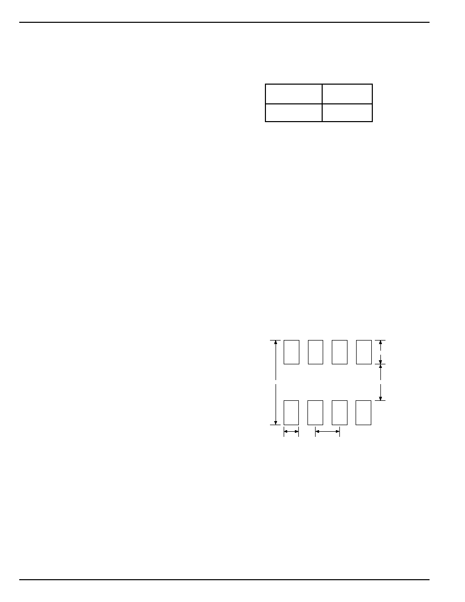
Part I. Layout
The MIC5202-xxBM (8-pin surface mount package) has the
following thermal characteristics when mounted on a single
layer copper-clad printed circuit board.
245 mil
30 mil
50 mil
50 mil
150 mil
Minimum recommended board pad size, SO-8.

MIC5202
Micrel
July 1998
7
MIC5202
Package Information
45
∞
0
∞
≠8
∞
0.244 (6.20)
0.228 (5.79)
0.197 (5.0)
0.189 (4.8)
SEATING
PLANE
0.026 (0.65)
MAX
)
0.010 (0.25)
0.007 (0.18)
0.064 (1.63)
0.045 (1.14)
0.0098 (0.249)
0.0040 (0.102)
0.020 (0.51)
0.013 (0.33)
0.157 (3.99)
0.150 (3.81)
0.050 (1.27)
TYP
PIN 1
DIMENSIONS:
INCHES (MM)
0.050 (1.27)
0.016 (0.40)
8-Pin SOP (M)

MIC5202
Micrel
MIC5202
8
July 1998
MICREL INC.
1849 FORTUNE DRIVE
SAN JOSE, CA 95131
USA
TEL
+ 1 (408) 944-0800
FAX
+ 1 (408) 944-0970
WEB
http://www.micrel.com
This information is believed to be accurate and reliable, however no responsibility is assumed by Micrel for its use nor for any infringement of patents or
other rights of third parties resulting from its use. No license is granted by implication or otherwise under any patent or patent right of Micrel Inc.
© 1998 Micrel Incorporated