MIC5206
Micrel
January 2000
1
MIC5206
General Description
The MIC5206 is an efficient linear voltage regulator with very
low dropout voltage (typically 17mV at light loads and 165mV
at 150mA), and very low ground current (600
µ
A at 100mA
output), with better than 1% initial accuracy. It has a logic
compatible enable/shutdown control input and an internal
undervoltage monitor.
Designed especially for hand-held, battery-powered devices,
the MIC5206 can be switched by a CMOS or TTL compatible
logic signal. When disabled, power consumption drops
nearly to zero. Dropout ground current is minimized to
prolong battery life.
Key features include an undervoltage monitor with an error
flag output, a reference bypass pin to improve its already low-
noise performance (8-lead versions only), reversed-battery
protection, current limiting, and overtemperature shutdown.
The MIC5206 is available in several fixed voltages in a tiny
SOT-23-5 package. It features a pinout, similar to the LP2980,
but has significantly better performance. Fixed and adjust-
able output voltage versions, featuring the reference bypass
option, are available in the 8-lead Micrel Mini 8TM 8-lead
MSOP (micro small-outline package).
For low-dropout regulators that are stable with ceramic
output capacitors, see the
µ
Cap MIC5245/6/7 family.
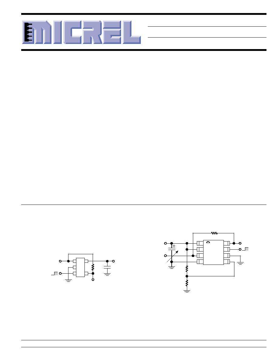
1
5
2
3
4
C
OUT
1µF tantalum
Enable
Shutdown
V
OUT
MIC5206-x.xBM5
Enable (pin 3) may be
connected directly to
Supply Input (pin 1).
V
IN
100k
Flag Output
(optional)
Typical Applications
1
2
3
4
8
7
6
5
1µF
V
OUT
Flag Output
(optional)
47k
R1
R2
MIC5206BMM
V
IN
Enable (pin 7) may be
connected directly to
Supply Input (pin 8).
Enable
Shutdown
tantalum
SOT-23-5 Fixed Voltage Application
Adjustable Voltage Application
MIC5206
150mA Low-Noise LDO Regulator
Features
∑ Error flag indicates undervoltage fault
∑ High output voltage accuracy
∑ Guaranteed 150mA output
∑ Ultra-low-noise output (8-lead versions)
∑ Low quiescent current
∑ Low dropout voltage
∑ Extremely tight load and line regulation
∑ Very low temperature coefficient
∑ Current and thermal limiting
∑ Reversed-battery protection
∑ "Zero" off-mode current
∑ Logic-controlled electronic enable
Applications
∑ Cellular telephones
∑ Laptop, notebook, and palmtop computers
∑ Battery-powered equipment
∑ PCMCIA V
CC
and V
PP
regulation/switching
∑ Consumer/personal electronics
∑ SMPS post-regulator/dc-to-dc modules
∑ High-efficiency linear power supplies
Micrel, Inc. ∑ 1849 Fortune Drive ∑ San Jose, CA 95131 ∑ USA ∑ tel + 1 (408) 944-0800 ∑ fax + 1 (408) 944-0970 ∑ http://www.micrel.com
Micrel Mini 8TM is a trademark of Micrel, Inc.
MIC5206
Micrel
MIC5206
2
January 2000
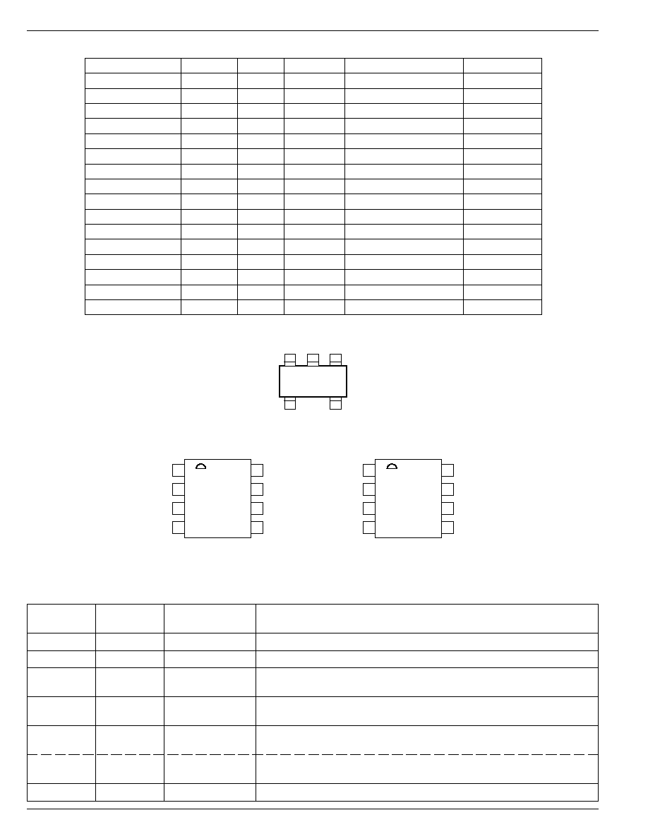
Pin Configuration
Ordering Information
Part Number
Marking
Volts
Accuracy
Junction Temp. Range
Package
MIC5206-2.5BM5
LD25
2.5
1%
≠40
∞
C to +125
∞
C
SOT-23-5
MIC5206-2.7BM5
LD27
2.7
1%
≠40
∞
C to +125
∞
C
SOT-23-5
MIC5206-3.0BM5
LD30
3.0
1%
≠40
∞
C to +125
∞
C
SOT-23-5
MIC5206-3.2BM5
LD32
3.2
1%
≠40
∞
C to +125
∞
C
SOT-23-5
MIC5206-3.3BM5
LD33
3.3
1%
≠40
∞
C to +125
∞
C
SOT-23-5
MIC5206-3.6BM5
LD36
3.6
1%
≠40
∞
C to +125
∞
C
SOT-23-5
MIC5206-3.8BM5
LD38
3.8
1%
≠40
∞
C to +125
∞
C
SOT-23-5
MIC5206-4.0BM5
LD40
4.0
1%
≠40
∞
C to +125
∞
C
SOT-23-5
MIC5206-5.0BM5
LD50
5.0
1%
≠40
∞
C to +125
∞
C
SOT-23-5
MIC5206BMM
--
Adj
1%
≠40
∞
C to +125
∞
C
8-lead MSOP
MIC5206-3.0BMM
--
3.0
1%
≠40
∞
C to +125
∞
C
8-lead MSOP
MIC5206-3.3BMM
--
3.3
1%
≠40
∞
C to +125
∞
C
8-lead MSOP
MIC5206-3.6BMM
--
3.6
1%
≠40
∞
C to +125
∞
C
8-lead MSOP
MIC5206-3.8BMM
--
3.8
1%
≠40
∞
C to +125
∞
C
8-lead MSOP
MIC5206-4.0BMM
--
4.0
1%
≠40
∞
C to +125
∞
C
8-lead MSOP
MIC5206-5.0BMM
--
5.0
1%
≠40
∞
C to +125
∞
C
8-lead MSOP
Other voltages available. Contact Micrel for details.
Pin Description
MIC5206
MIC5206
Pin Name
Pin Function
SOT-23-5
MSOP-8
1
8
IN
Supply Input
2
4, 6
GND
Ground
3
7
EN
Enable/Shutdown (Input): CMOS compatible input. Logic high = enable,
logic low or open = shutdown. Do not leave floating.
4
3
FLAG
Error Flag (Output): Open-collector output. Active low indicates an ouput
undervoltage condition.
5 (fixed)
BYP
Reference Bypass: Connect external 470pF capacitor to GND to reduce
output noise. May be left open.
5 (adj.)
ADJ
Adjust (Input): Adjustable regulator feedback input. Connect to resistor
voltage divider.
5
1,2
OUT
Regulator Output
IN
OUT
FLAG
EN
LDxx
1
3
4
5
2
GND
1
2
3
4
8
7
6
5
IN
EN
GND
ADJ
OUT
OUT
FLAG
GND
1
2
3
4
8
7
6
5
IN
EN
GND
BYP
OUT
OUT
FLAG
GND
MIC5206-xxBM5
(Fixed Output Voltage)
MIC5206-x.xBMM
(Fixed Output Voltage)
MIC5206BMM
(Adjustable Ouput Voltage)

MIC5206
Micrel
January 2000
3
MIC5206
Absolute Maximum Ratings
(Note 1)
Supply Input Voltage (V
IN
) ............................ ≠20V to +20V
Enable Input Voltage (V
EN
) ........................... ≠20V to +20V
Power Dissipation (P
D
) ............... Internally Limited, Note 3
Junction Temperature (T
J
) ....................... ≠40
∞
C to +125
∞
C
Lead Temperature (Soldering, 5 sec.) ...................... 260
∞
C
Electrical Characteristics
V
IN
= V
OUT
+ 1V; I
L
= 100
µ
A; C
L
= 1.0
µ
F; V
EN
2.0V; T
J
= 25
∞
C, bold values indicate ≠40
∞
C
T
J
+125
∞
C; unless noted.
Symbol
Parameter
Conditions
Min
Typical
Max
Units
V
O
Output Voltage Accuracy
variation from nominal V
OUT
≠1
1
%
≠2
2
%
V
O
/
T
Output Voltage
Note 4
40
ppm/
∞
C
Temperature Coefficient
V
O
/V
O
Line Regulation
V
IN
= V
OUT
+ 1V to 16V
0.004
0.012
% / V
V
O
/V
O
Load Regulation
I
L
= 0.1mA to 150mA, Note 5
0.02
0.2
%
V
IN
≠ V
O
Dropout Voltage, Note 6
I
L
= 100
µ
A
17
50
mV
70
mV
I
L
= 50mA
110
150
mV
230
mV
I
L
= 100mA
140
250
mV
300
mV
I
L
= 150mA
165
275
mV
350
mV
I
GND
Quiescent Current
V
EN
0.4V (shutdown)
0.01
1
µ
A
V
EN
0.18V (shutdown)
5
µ
A
I
GND
Ground Pin Current, Note 7
V
EN
2.0V, I
L
= 100
µ
A
80
125
µ
A
150
µ
A
I
L
= 50mA
350
600
µ
A
800
µ
A
I
L
= 100mA
600
1000
µ
A
1500
µ
A
I
L
= 150mA
1300
1900
µ
A
2500
µ
A
PSRR
Ripple Rejection
75
dB
I
LIMIT
Current Limit
V
OUT
= 0V
320
500
mA
V
O
/
P
D
Thermal Regulation
Note 8
0.05
%/W
e
no
Output Noise
I
L
= 50mA, C
L
= 4.7
µ
F, 470pF from BYP
260
nV Hz
to GND (MM package only)
Enable Input
V
IL
Enable Input Logic-Low Voltage
regulator shutdown
0.4
V
0.18
V
V
IH
Enable Input Logic-High Voltage
regulator enabled
2.0
V
I
IL
Enable Input Current
V
IL
0.4V
0.01
≠1
µ
A
V
IL
0.18V
≠2
µ
A
I
IH
V
IH
2.0V
5
20
µ
A
V
IH
2.0V
25
µ
A
Error Flag Output
V
ERR
Flag Threshold
undervoltage condition (below nominal)
≠2
≠6
≠10
%
Note 9
V
OL
Output Logic-Low Voltage
I
L
= 1mA, undervoltage condition
0.2
0.4
V
I
FL
Flag Leakage Current
flag off, V
FLAG
= 0V to 16V
≠1
0.1
+1
µ
A
Operating Ratings
(Note 2)
Supply Input Voltage (V
IN
) ........................... +2.5V to +16V
Enable Input Voltage (V
EN
) .................................. 0V to V
IN
Junction Temperature (T
J
) ....................... ≠40
∞
C to +125
∞
C
SOT-23-5 (
JA
) ......................................................... Note 3
8-lead MSOP (
JA
) ................................................... Note 3
MIC5206
Micrel
MIC5206
4
January 2000
Note 1:
Exceeding the absolute maximum rating may damage the device.
Note 2.
The device is not guaranteed to function outside its operating rating.
Note 3:
The maximum allowable power dissipation at any T
A
(ambient temperature) is P
D(max)
= (T
J(max)
≠ T
A
)
˜
JA
. Exceeding the maximum
allowable power dissipation will result in excessive die temperature, and the regulator will go into thermal shutdown. The
JA
of the
MIC5205-x.xBM5 (all versions) is 220
∞
C/W, and the MIC5206-x.xBMM (all versions) is 200
∞
C/W, mounted on a PC board (see "Thermal
Considerations" for further details).
Note 4:
Output voltage temperature coefficient is defined as the worst case voltage change divided by the total temperature range.
Note 5:
Regulation is measured at constant junction temperature using low duty cycle pulse testing. Parts are tested for load regulation in the load
range from 0.1mA to 150mA. Changes in output voltage due to heating effects are covered by the thermal regulation specification.
Note 6:
Dropout Voltage is defined as the input to output differential at which the output voltage drops 2% below its nominal value measured at 1V
differential.
Note 7:
Ground pin current is the regulator quiescent current plus pass transistor base current. The total current drawn from the supply is the sum of
the load current plus the ground pin current.
Note 8:
Thermal regulation is defined as the change in output voltage at a time "t" after a change in power dissipation is applied, excluding load or line
regulation effects. Specifications are for a 150mA load pulse at V
IN
= 16V for t = 10ms.
Note 9:
The error flag comparator includes 3% hysteresis.
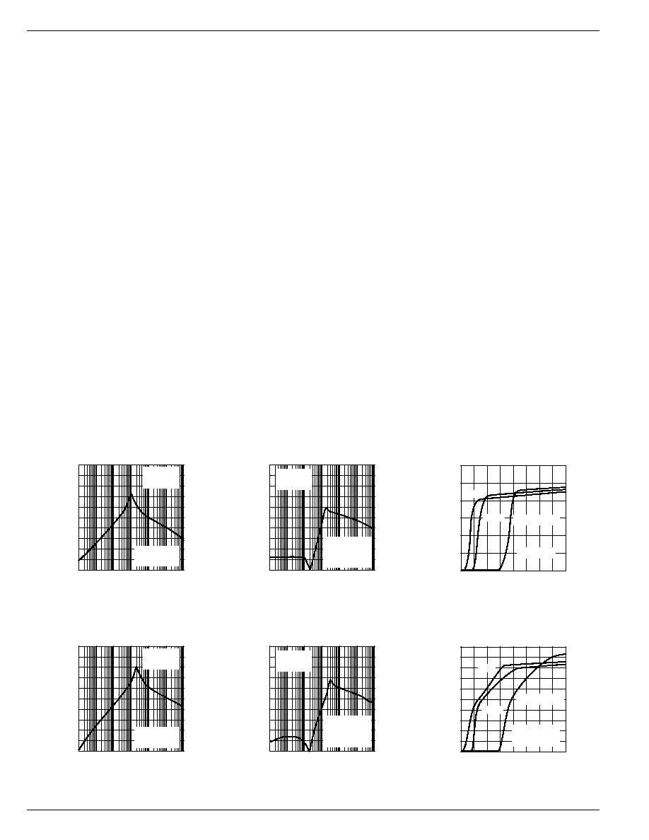
-100
-80
-60
-40
-20
0
1E+1 1E+2 1E+3 1E+4 1E+5 1E+6 1E+7
PSRR (dB)
FREQUENCY (Hz)
Power Supply
Rejection Ratio
I
OUT
= 100
µ
A
C
OUT
= 1
µ
F
V
IN
= 6V
V
OUT
= 5V
10
100
1k
10k 100k 1M 10M
-100
-80
-60
-40
-20
0
1E+1 1E+2 1E+3 1E+4 1E+5 1E+6 1E+7
PSRR (dB)
FREQUENCY (Hz)
Power Supply
Rejection Ratio
I
OUT
= 100
µ
A
C
OUT
= 2.2
µ
F
C
BYP
= 0.01
µ
F
V
IN
= 6V
V
OUT
= 5V
10
100
1k
10k 100k 1M 10M
0
10
20
30
40
50
60
0
0.1
0.2
0.3
0.4
RIPPLE REJECTION (dB)
VOLTAGE DROP (V)
Power Supply Ripple Rejection
vs. Voltage Drop
I
OUT
= 100mA
10mA
1mA
C
OUT
= 1
µ
F
-100
-80
-60
-40
-20
0
1E+1 1E+2 1E+3 1E+4 1E+5 1E+6 1E+7
PSRR (dB)
FREQUENCY (Hz)
Power Supply
Rejection Ratio
I
OUT
= 1mA
C
OUT
= 1
µ
F
V
IN
= 6V
V
OUT
= 5V
10
100
1k
10k 100k 1M 10M
-100
-80
-60
-40
-20
0
1E+1 1E+2 1E+3 1E+4 1E+5 1E+6 1E+7
PSRR (dB)
FREQUENCY (Hz)
Power Supply
Rejection Ratio
I
OUT
= 1mA
C
OUT
= 2.2
µ
F
C
BYP
= 0.01
µ
F
V
IN
= 6V
V
OUT
= 5V
10
100
1k
10k 100k 1M 10M
0
10
20
30
40
50
60
70
80
90
100
0
0.1
0.2
0.3
0.4
RIPPLE REJECTION (dB)
VOLTAGE DROP (V)
Power Supply Ripple Rejection
vs. Voltage Drop
I
OUT
= 100mA
10mA
1mA
C
OUT
= 2.2
µ
F
C
BYP
= 0.01
µ
F
Typical Characteristics
MIC5206
Micrel
January 2000
5
MIC5206
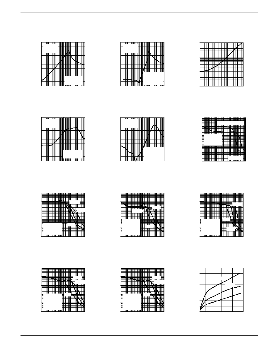
Typical Characteristics
-100
-80
-60
-40
-20
0
1E+1 1E+2 1E+3 1E+4 1E+5 1E+6 1E+7
PSRR (dB)
FREQUENCY (Hz)
Power Supply
Rejection Ratio
I
OUT
= 10mA
C
OUT
= 1
µ
F
V
IN
= 6V
V
OUT
= 5V
10
100
1k
10k 100k 1M 10M
-100
-80
-60
-40
-20
0
1E+1 1E+2 1E+3 1E+4 1E+5 1E+6 1E+7
PSRR (dB)
FREQUENCY (Hz)
Power Supply
Rejection Ratio
I
OUT
= 10mA
C
OUT
= 2.2
µ
F
C
BYP
= 0.01
µ
F
V
IN
= 6V
V
OUT
= 5V
10
100
1k
10k 100k 1M 10M
10
100
1000
10000
10
100
1000
10000
TIME (
µ
s)
CAPACITANCE (pF)
Turn-On Time
vs. Bypass Capacitance
-100
-80
-60
-40
-20
0
1E+1 1E+2 1E+3 1E+4 1E+5 1E+6 1E+7
PSRR (dB)
FREQUENCY (Hz)
Power Supply
Rejection Ratio
I
OUT
= 100mA
C
OUT
= 1
µ
F
V
IN
= 6V
V
OUT
= 5V
10
100
1k
10k 100k 1M 10M
-100
-80
-60
-40
-20
0
1E+1 1E+2 1E+3 1E+4 1E+5 1E+6 1E+7
PSRR (dB)
FREQUENCY (Hz)
Power Supply
Rejection Ratio
I
OUT
= 100mA
C
OUT
= 2.2
µ
F
C
BYP
= 0.01
µ
F
V
IN
= 6V
V
OUT
= 5V
10
100
1k
10k 100k 1M 10M
0.0001
0.001
0.01
0.1
1
10
1E+1 1E+2 1E+3 1E+4 1E+5 1E+6 1E+7
NOISE (
µ
V/
Hz)
FREQUENCY (Hz)
Noise Performance
10
100
1k
10k 100k 1M 10M
1mA
C
OUT
= 1
µ
F
C
BYP
= 10nF
10mA, C
OUT
= 1
µ
F
V
OUT
= 5V
0.0001
0.001
0.01
0.1
1
10
1E+1 1E+2 1E+3 1E+4 1E+5 1E+6 1E+7
NOISE (
µ
V/
Hz)
FREQUENCY (Hz)
Noise Performance
10mA
1mA
100mA
10
100
1k
10k 100k 1M 10M
V
OUT
= 5V
C
OUT
= 10
µ
F
electrolytic
0.0001
0.001
0.01
0.1
1
10
1E+1 1E+2 1E+3 1E+4 1E+5 1E+6 1E+7
NOISE (
µ
V/
Hz)
FREQUENCY (Hz)
Noise Performance
10mA
1mA
100mA
10
100
1k
10k 100k 1M 10M
V
OUT
= 5V
C
OUT
= 22
µ
F
tantalum
C
BYP
= 10nF
0.0001
0.001
0.01
0.1
1
10
1E+1 1E+2 1E+3 1E+4 1E+5 1E+6 1E+7
NOISE (
µ
V/
Hz)
FREQUENCY (Hz)
Noise Performance
10mA
1mA
100mA
10
100
1k
10k 100k 1M 10M
V
OUT
= 5V
C
OUT
= 10
µ
F
electrolytic
C
BYP
= 100pF
0.0001
0.001
0.01
0.1
1
10
1E+1 1E+2 1E+3 1E+4 1E+5 1E+6 1E+7
NOISE (
µ
V/
Hz)
FREQUENCY (Hz)
Noise Performance
10mA
1mA
100mA
10
100
1k
10k 100k 1M 10M
V
OUT
= 5V
C
OUT
= 10
µ
F
electrolytic
C
BYP
= 1nF
0.0001
0.001
0.01
0.1
1
10
1E+1 1E+2 1E+3 1E+4 1E+5 1E+6 1E+7
NOISE (
µ
V/
Hz)
FREQUENCY (Hz)
Noise Performance
10mA
1mA
100mA
10
100
1k
10k 100k 1M 10M
V
OUT
= 5V
C
OUT
= 10
µ
F
electrolytic
C
BYP
= 1nF
0
40
80
120
160
200
240
280
320
0
40
80
120
160
DROPOUT VOLTAGE (mV)
OUTPUT CURRENT (mA)
Dropout Voltage
vs. Output Current
+125
∞
C
+25
∞
C
≠40
∞
C