3-168
1997
MIC5208
Micrel
MIC5208
Dual 50mA LDO Voltage Regulator
Preliminary Information
General Description
The MIC5208 is a dual linear voltage regulator with very low
dropout voltage (typically 20mV at light loads and 250mV at
50mA), very low ground current (225
µ
A at 10mA output), and
better than 3% initial accuracy. It also features individual
logic-compatible enable/shutdown control inputs.
Designed especially for hand-held battery powered devices,
the MIC5208 can be switched by a CMOS or TTL compatible
logic signal, or the enable pin can be connected to the supply
input for 3-terminal operation. When disabled, power con-
sumption drops nearly to zero. Dropout ground current is
minimized to prolong battery life.
Key features include current limiting, overtemperature shut-
down, and protection against reversed battery.
The MIC5208 is available in 3.0V, 3.3V, 3.6V, 4.0V and 5.0V
fixed voltage configurations. Other voltages are available;
contact Micrel for details.
Features
∑ Micrel Mini 8TM MSOP package
∑ Guaranteed 50mA output
∑ Low quiescent current
∑ Low dropout voltage
∑ Wide selection of output voltages
∑ Tight load and line regulation
∑ Low temperature coefficient
∑ Current and thermal limiting
∑ Reversed input polarity protection
∑ Zero off-mode current
∑ Logic-controlled electronic enable
Applications
∑ Cellular telephones
∑ Laptop, notebook, and palmtop computers
∑ Battery powered equipment
∑ Bar code scanners
∑ SMPS post regulator/dc-to-dc modules
∑ High-efficiency linear power supplies
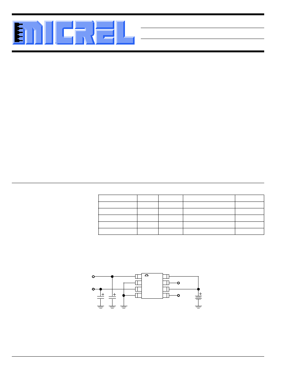
1
2
3
4
8
7
6
5
Output A
MIC5208
1µF
Enable may be connected to VIN
Enable A
Enable B
1µF
Output B
Typical Application
Ordering Information
Part Number
Voltage
Accuracy
Junction Temp. Range*
Package
MIC5208-3.0BMM
3.0
3%
≠40
∞
C to +125
∞
C
8-lead MSOP
MIC5208-3.3BMM
3.3
3%
≠40
∞
C to +125
∞
C
8-lead MSOP
MIC5208-3.6BMM
3.6
3%
≠40
∞
C to +125
∞
C
8-lead MSOP
MIC5208-4.0BMM
4.0
3%
≠40
∞
C to +125
∞
C
8-lead MSOP
MIC5208-5.0BMM
5.0
3%
≠40
∞
C to +125
∞
C
8-lead MSOP
Other voltages available. Contact Micrel for details.
3-170
1997
MIC5208
Micrel
Absolute Maximum Ratings
Supply Input Voltage (V
IN
) ............................ ≠20V to +20V
Enable Input Voltage (V
EN
) ........................... ≠20V to +20V
Power Dissipation (P
D
) ............................ Internally Limited
Storage Temperature Range ................... ≠60
∞
C to +150
∞
C
Lead Temperature (soldering, 5 sec.) ....................... 260
∞
C
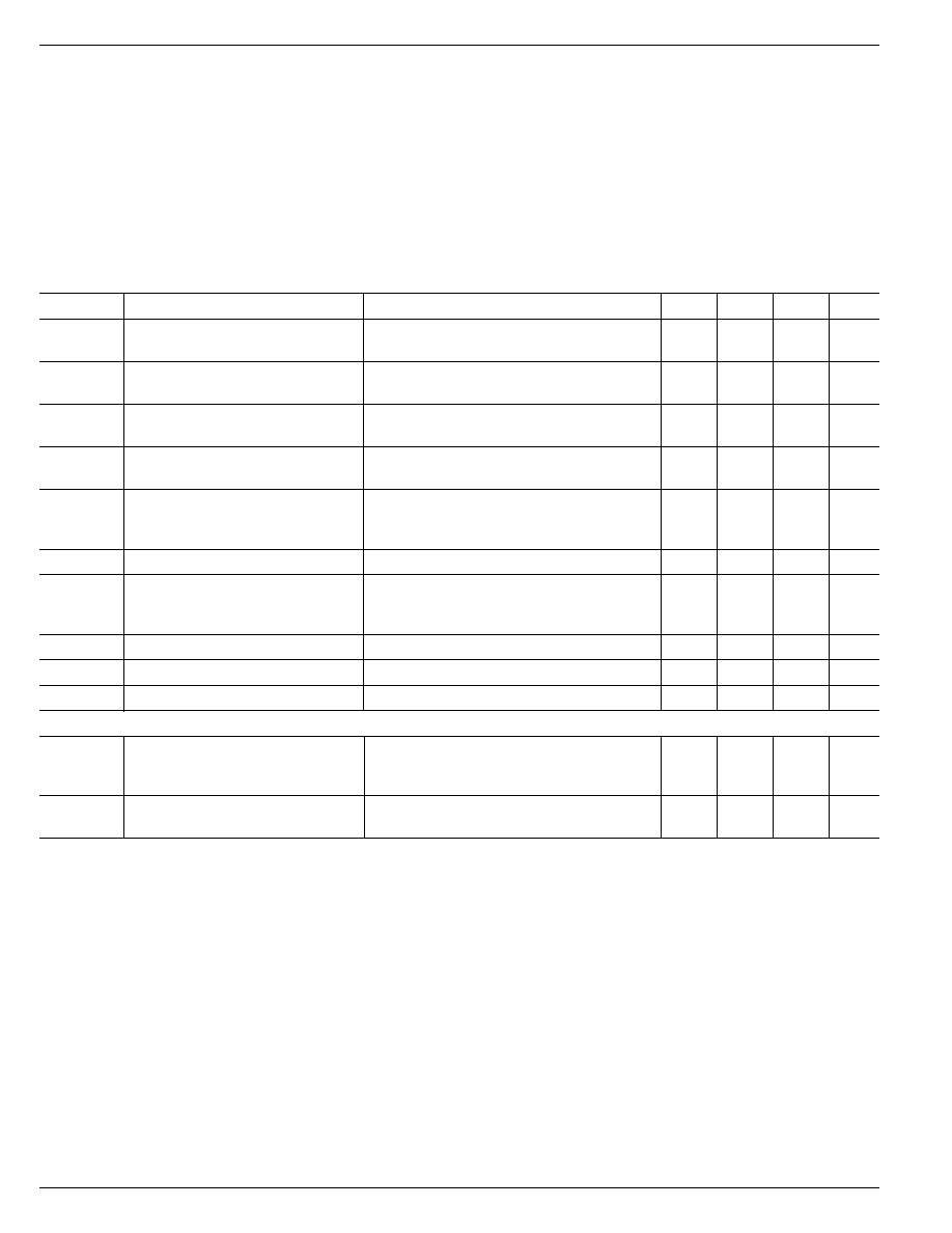
Electrical Characteristics
V
IN
= V
OUT
+ 1V; I
L
= 1mA; C
L
= 1
µ
F, and V
EN
2.0V; T
J
= 25
∞
C, bold values indicate ≠40
∞
C to +125
∞
C;
for one-half of dual MIC5208; unless noted.
Symbol
Parameter
Conditions
Min
Typical
Max
Units
V
O
Output Voltage
variation from nominal V
OUT
≠3
3
%
Accuracy
≠4
4
%
V
O
/
T
Output Voltage
Note 2
50
200
ppm/
∞
C
Temperature Coeffcient
V
O
/V
O
Line Regulation
V
IN
= V
OUT
+1V to 16V
0.008
0.3
%
0.5
%
V
O
/V
O
Load Regulation
I
L
= 0.1mA to 50mA, Note 3
0.08
0.3
%
0.5
%
V
IN
≠ V
O
Dropout Voltage, Note 4
I
L
= 100
µ
A
20
mV
I
L
= 20mA
200
350
mV
I
L
= 50mA
250
500
mV
I
Q
Quiescent Current
V
EN
0.4V (shutdown)
0.01
10
µ
A
I
GND
Ground Pin Current
V
EN
2.0V (enabled), I
L
= 100
µ
A
180
µ
A
Note 5
I
L
= 20mA
225
750
µ
A
I
L
= 50mA
850
1200
µ
A
I
GNDDO
Ground Pin Current at Dropout
V
IN
= 0.5V less than designed V
OUT
,
Note 5
200
300
µ
A
I
LIMIT
Current Limit
V
OUT
= 0V
180
250
mA
V
O
/
P
D
Thermal Regulation
Note 6
0.05
%/W
Control Input
Input Voltage Level
V
IL
Logic Low
shutdown
0.6
V
V
IH
Logic High
enabled
2.0
V
I
IL
Control Input Current
V
IL
0.6V
0.01
1
µ
A
I
IH
V
IH
2.0V
15
50
µ
A
General Note:
Devices are ESD protected, however, handling precautions are recommended.
Note 1:
Absolute maximum ratings indicate limits beyond which damage to the component may occur. Electrical specifications do not apply when
operating the device outside of its rated operating conditions. The maximum allowable power dissipation is a function of the maximum
junction temperature, T
J(max)
, the junction-to-ambient thermal resistance,
JA
, and the ambient temperature, T
A
. The maximum allowable
power dissipation at any ambient temperature is calculated using: P
MAX
= (T
J(max)
≠ T
A
)
/
JA
. Exceeding the maximum allowable power
dissipation will result in excessive die temperature, and the regulator will go into thermal shutdown.
JA
of the 8-lead MSOP is 200
∞
C/W,
mounted on a PC board.
Note 2:
Output voltage temperature coefficient is defined as the worst case voltage change divided by the total temperature range.
Note 3:
Regulation is measured at constant junction temperature using low duty cycle pulse testing. Changes in output voltage due to heating effects
are covered by the thermal regulation specification.
Note 4:
Dropout voltage is defined as the input to output differential at which the output voltage drops 2% below its nominal value measured at 1V
differential.
Note 5:
Ground pin current is the regulator quiescent current plus pass transistor base current. The total current drawn from the supply is the sum of
the load current plus the ground pin current.
Note 6:
Thermal regulation is defined as the change in output voltage at a time "t" after a change in power dissipation is applied, excluding load or line
regulation effects. Specifications are for a 50mA load pulse at V
IN
= 16V for t = 10ms.
Recommended Operating Conditions
Supply Input Voltage (V
IN
) ............................... 2.5V to 16V
Enable Input Voltage (V
EN
) ................................. 0V to 16V
Junction Temperature (T
J
) ....................... ≠40
∞
C to +125
∞
C
8-lead MSOP
(
JA
) ................................................... Note 1