April 1997∑
1
MIC5210
MIC5210
Micrel
MIC5210
Dual 100mA LDO Regulator
Advance Information
General Description
The MIC5210 is a dual linear voltage regulator with very low
dropout voltage (typically 10mV at light loads and 140mV at
100mA), very low ground current (225
µ
A at 10mA output), and
better than 3% initial accuracy. It also features individual
logic-compatible enable/shutdown control inputs.
Designed especially for hand-held battery powered devices,
the MIC5210 can be switched by a CMOS or TTL compatible
logic signal, or the enable pin can be connected to the supply
input for 3-terminal operation. When disabled, power con-
sumption drops nearly to zero. Dropout ground current is
minimized to prolong battery life.
Key features include current limiting, overtemperature shut-
down, and protection against reversed battery.
The MIC5210 is available in 3.0V, 3.3V, 3.6V, 4.0V and 5.0V
fixed voltage configurations. Other voltages are available;
contact Micrel for details.
Features
∑ Micrel Mini 8TM MSOP package
∑ Guaranteed 100mA outputs
∑ Low quiescent current
∑ Low dropout voltage
∑ Wide selection of output voltages
∑ Tight load and line regulation
∑ Low temperature coefficient
∑ Current and thermal limiting
∑ Reversed input polarity protection
∑ Zero off-mode current
∑ Logic-controlled electronic enable
Applications
∑ Cellular telephones
∑ Laptop, notebook, and palmtop computers
∑ Battery powered equipment
∑ Bar code scanners
∑ SMPS post regulator/dc-to-dc modules
∑ High-efficiency linear power supplies
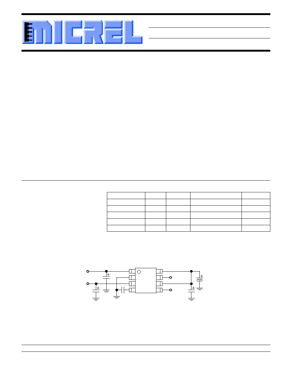
Typical Application
1
2
3
4
8
7
6
5
Output A
MIC5210
2.2µF
Enable may be connected to VIN
Enable A
Enable B
1µF
Output B
C
BYP
470µF
1µF
Low-Noise + Ultralow-Noise (Dual) Regulator
Ordering Information
Part Number
Voltage
Accuracy
Junction Temp. Range*
Package
MIC5210-3.0BMM
3.0
1.0%
≠40
∞
C to +125
∞
C
8-lead MSOP
MIC5210-3.3BMM
3.3
1.0%
≠40
∞
C to +125
∞
C
8-lead MSOP
MIC5210-3.6BMM
3.6
1.0%
≠40
∞
C to +125
∞
C
8-lead MSOP
MIC5210-4.0BMM
4.0
1.0%
≠40
∞
C to +125
∞
C
8-lead MSOP
MIC5210-5.0BMM
5.0
1.0%
≠40
∞
C to +125
∞
C
8-lead MSOP
Other voltages available. Contact Micrel for details.
Micrel, Inc. ∑ 1849 Fortune Drive ∑ San Jose, CA 95131 ∑ USA ∑ tel + 1 (408) 944-0800 ∑ fax + 1 (408) 944-0970 ∑ http://www.micrel.com
MM8 and Micrel Mini 8 are trademarks of Micrel, Inc.
MIC5210
2
April 1997∑
MIC5210
Micrel
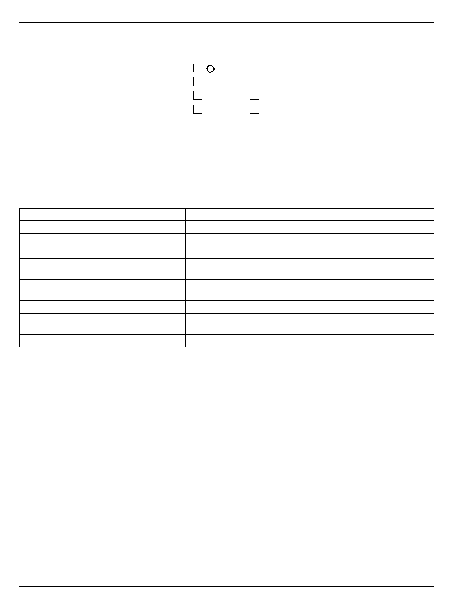
Pin Configuration
1
2
3
4
8
7
6
5
INA
ENA
INB
ENB
OUTA
GND
OUTB
BYPB
MIC5210BMM
Pin Description
Pin Number
Pin Name
Pin Function
1
OUTA
Regulator Output A
2
GND
Ground: Both pins must be connected together.
3
OUTB
Regulator Output B
4
BYPB
Reference Bypass B: Connect external 470pF capacitor to GND to reduce
output noise in regulator "B". May be left open.
5
ENB
Enable/Shutdown B (Input): CMOS compatible input. Logic high = enable,
logic low or open = shutdown. Do not leave floating.
6
INB
Supply Input B
7
ENA
Enable/Shutdown A (Input): CMOS compatible input. Logic high = enable,
logic low or open = shutdown. Do not leave floating.
8
INA
Supply Input A
Absolute Maximum Ratings
Supply Input Voltage (V
IN
) ............................ ≠20V to +20V
Enable Input Voltage (V
EN
) ........................... ≠20V to +20V
Power Dissipation (P
D
) ............................ Internally Limited
Storage Temperature Range ................... ≠60
∞
C to +150
∞
C
Lead Temperature (soldering, 5 sec.) ....................... 260
∞
C
Recommended Operating Conditions
Supply Input Voltage (V
IN
) ............................... 2.5V to 16V
Enable Input Voltage (V
EN
) ................................. 0V to 16V
Junction Temperature (T
J
) ....................... ≠40
∞
C to +125
∞
C
8-lead MSOP
(
JA
) ................................................... Note 1
April 1997∑
3
MIC5210
MIC5210
Micrel
Electrical Characteristics
V
IN
= V
OUT
+ 1V; I
L
= 100
µ
A; C
L
= 1.0
µ
F; V
EN
2.0V; T
J
= 25
∞
C, bold values indicate ≠40
∞
C
T
J
+125
∞
C; unless noted.
Symbol
Parameter
Conditions
Min
Typical
Max
Units
V
O
Output Voltage Accuracy
variation from specified V
OUT
≠1
1
%
≠2
2
%
V
O
/
T
Output Voltage
Note 2
40
ppm/
∞
C
Temperature Coefficient
V
O
/V
O
Line Regulation
V
IN
= V
OUT
+ 1V to 16V
0.004
0.012
% / V
0.05
% / V
V
O
/V
O
Load Regulation
I
L
= 0.1mA to 150mA (Note 3)
0.02
0.2
%
0.5
%
V
IN
≠ V
O
Dropout Voltage, Note 4
I
L
= 100
µ
A
10
50
mV
70
mV
I
L
= 50mA
110
150
mV
230
mV
I
L
= 100mA
140
250
mV
300
mV
I
L
= 150mA
165
275
mV
350
mV
I
GND
Quiescent Current
V
EN
0.4V (shutdown)
0.01
1
µ
A
V
EN
0.18V (shutdown)
5
µ
A
I
GND
Ground Pin Current, Note 5
V
EN
2.0V, I
L
= 100
µ
A
80
125
µ
A
150
µ
A
I
L
= 50mA
350
600
µ
A
800
µ
A
I
L
= 100mA
600
1000
µ
A
1500
µ
A
I
L
= 150mA
1300
1900
µ
A
2500
µ
A
PSRR
Ripple Rejection
frequency = 100Hz, I
L
= 100
µ
A
75
500
dB
I
LIMIT
Current Limit
V
OUT
= 0V
320
500
mA
V
O
/
P
D
Thermal Regulation
Note 6
0.05
%/W
e
no
Output Noise
I
L
= 50mA, C
L
= 2.2
µ
F,
260
nV Hz
470pF from BYP to GND
ENABLE Input
V
IL
Enable Input Logic-Low Voltage
regulator shutdown
0.4
V
0.18
V
V
IH
Enable Input Logic-High Voltage
regulator enabled
2.0
V
I
IL
Enable Input Current
V
IL
0.4V
0.01
≠1
µ
A
V
IL
0.18V
≠2
µ
A
I
IH
V
IH
2.0V
5
20
µ
A
V
IH
2.0V
25
µ
A
Note 1:
Absolute maximum ratings indicate limits beyond which damage to the component may occur. Electrical specifications do not apply when
operating the device outside of its operating ratings. The maximum allowable power dissipation is a function of the maximum junction
temperature, T
J(max)
, the junction-to-ambient thermal resistance,
JA
, and the ambient temperature, T
A
. The maximum allowable power
dissipation at any ambient temperature is calculated using: P
D(max)
= (T
J(max)
≠ T
A
)
JA
. Exceeding the maximum allowable power dissipation
will result in excessive die temperature, and the regulator will go into thermal shutdown. The
JA
of the 8-lead MSOP (MM) is 200
∞
C/W
mounted on a PC board (see "Thermal Considerations" section for further details).
Note 2:
Output voltage temperature coefficient is defined as the worst case voltage change divided by the total temperature range.
Note 3:
Regulation is measured at constant junction temperature using low duty cycle pulse testing. Parts are tested for load regulation in the load
range from 0.1mA to 150mA. Changes in output voltage due to heating effects are covered by the thermal regulation specification.
Note 4:
Dropout Voltage is defined as the input to output differential at which the output voltage drops 2% below its nominal value measured at 1V
differential.
Note 5:
Ground pin current is the regulator quiescent current plus pass transistor base current. The total current drawn from the supply is the sum of
the load current plus the ground pin current.
Note 6:
Thermal regulation is defined as the change in output voltage at a time "t" after a change in power dissipation is applied, excluding load or line
regulation effects. Specifications are for a 150mA load pulse at V
IN
= 16V for t = 10ms.
MIC5210
4
April 1997∑
MIC5210
Micrel
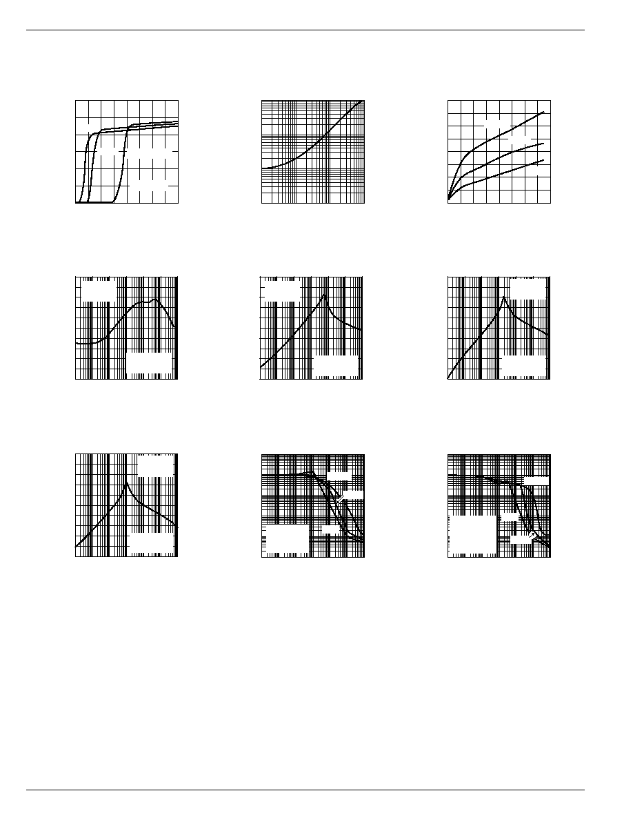
Typical Characteristics
0
10
20
30
40
50
60
0
0.1
0.2
0.3
0.4
RIPPLE REJECTION (dB)
VOLTAGE DROP (V)
Power Supply Ripple Rejection
vs. Voltage Drop
I
OUT
= 100mA
10mA
1mA
C
OUT
= 1
µ
F
10
100
1000
10000
10
100
1000
10000
TIME (
µ
s)
CAPACITANCE (pF)
Turn-On Time
vs. Bypass Capacitance
0
40
80
120
160
200
240
280
320
0
40
80
120
160
DROPOUT VOLTAGE (mV)
OUTPUT CURRENT (mA)
Dropout Voltage
vs. Output Current
+125
∞
C
+25
∞
C
≠40
∞
C
-100
-80
-60
-40
-20
0
1E+1 1E+2 1E+3 1E+4 1E+5 1E+6 1E+7
PSRR (dB)
FREQUENCY (Hz)
Power Supply
Rejection Ratio
I
OUT
= 100mA
C
OUT
= 1
µ
F
V
IN
= 6V
V
OUT
= 5V
10
100
1k
10k 100k 1M 10M
-100
-80
-60
-40
-20
0
1E+1 1E+2 1E+3 1E+4 1E+5 1E+6 1E+7
PSRR (dB)
FREQUENCY (Hz)
Power Supply
Rejection Ratio
I
OUT
= 10mA
C
OUT
= 1
µ
F
V
IN
= 6V
V
OUT
= 5V
10
100
1k
10k 100k 1M 10M
0.0001
0.001
0.01
0.1
1
10
1E+1 1E+2 1E+3 1E+4 1E+5 1E+6 1E+7
NOISE (
µ
V/
Hz)
FREQUENCY (Hz)
Noise Performance
10mA
1mA
100mA
10
100
1k
10k 100k 1M 10M
V
OUT
= 5V
C
OUT
= 10
µ
F
electrolytic
C
BYP
= 100pF
-100
-80
-60
-40
-20
0
1E+1 1E+2 1E+3 1E+4 1E+5 1E+6 1E+7
PSRR (dB)
FREQUENCY (Hz)
Power Supply
Rejection Ratio
I
OUT
= 1mA
C
OUT
= 1
µ
F
V
IN
= 6V
V
OUT
= 5V
10
100
1k
10k 100k 1M 10M
-100
-80
-60
-40
-20
0
1E+1 1E+2 1E+3 1E+4 1E+5 1E+6 1E+7
PSRR (dB)
FREQUENCY (Hz)
Power Supply
Rejection Ratio
I
OUT
= 100
µ
A
C
OUT
= 1
µ
F
V
IN
= 6V
V
OUT
= 5V
10
100
1k
10k 100k 1M 10M
0.0001
0.001
0.01
0.1
1
10
1E+1 1E+2 1E+3 1E+4 1E+5 1E+6 1E+7
NOISE (
µ
V/
Hz)
FREQUENCY (Hz)
Noise Performance
10mA
1mA
100mA
10
100
1k
10k 100k 1M 10M
V
OUT
= 5V
C
OUT
= 10
µ
F
electrolytic
April 1997∑
5
MIC5210
MIC5210
Micrel
above 1MHz. Most tantalum or aluminum electrolytic capaci-
tors are adequate; film types will work, but are more expen-
sive. Since many aluminum electrolytics have electrolytes
that freeze at about ≠30
∞
C, solid tantalums are recommended
for operation below ≠25
∞
C.
At lower values of output current, less output capacitance is
required for output stability. The capacitor can be reduced to
0.47
µ
F for current below 10mA or 0.33
µ
F for currents below
1mA.
No-Load Stability
The MIC5210 will remain stable and in regulation with no load
(other than the internal voltage divider) unlike many other
voltage regulators. This is especially important in CMOS RAM
keep-alive applications.
Dual-Supply Operation
When used in dual supply systems where the regulator load
is returned to a negative supply, the output voltage must be
diode clamped to ground.
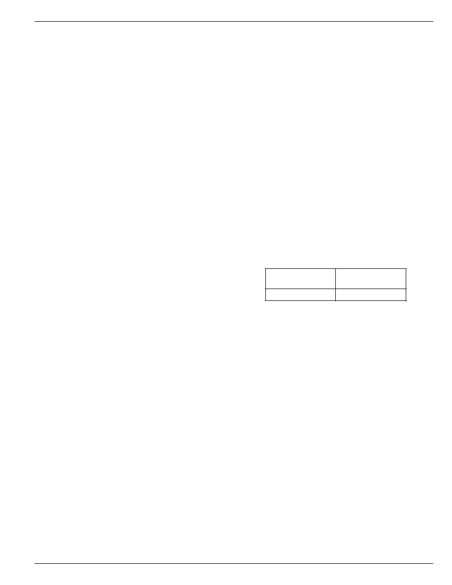
Thermal Considerations
Multilayer boards having a ground plane, wide traces near the
pads, and large supply bus lines provide better thermal
conductivity.
The MIC5210-xxBMM (8-lead MSOP) has a thermal resis-
tance of 200
∞
C/W when mounted on a FR4 board with
minimum trace widths and no ground plane.
PC Board
JA
Dielectric
FR4
200
∞
C
MSOP Thermal Characteristics
For additional heat sink characteristics, please refer to Micrel
Application Hint 17, "Calculating P.C. Board Heat Sink Area
For Surface Mount Packages".
Applications Information
Enable/Shutdown
Forcing EN (enable/shutdown) high (> 2V) enables the regu-
lator. EN is compatible with CMOS logic gates.
If the enable/shutdown feature is not required, connect EN to
IN (supply input).
Input Capacitor
A 1
µ
F capacitor should be placed from IN to GND if there is
more than 10 inches of wire between the input and the ac filter
capacitor or if a battery is used as the input.
Reference Bypass Capacitor
BYP (reference bypass) is connected to the internal voltage
reference. A 470pF capacitor (C
BYP
) connected from BYP to
GND quiets this reference, providing a significant reduction in
output noise. C
BYP
reduces the regulator phase margin; when
using C
BYP
, output capacitors of 2.2
µ
F or greater are gener-
ally required to maintain stability.
The start-up speed of the MIC5210 is inversely proportional to
the size of the reference bypass capacitor. Applications re-
quiring a slow ramp-up of output voltage should consider
larger values of C
BYP
. Likewise, if rapid turn-on is necessary,
consider omitting C
BYP
.
If output noise is not a major concern, omit C
BYP
and leave
BYP open.
Output Capacitor
An output capacitor is required between OUT and GND to
prevent oscillation. The minimum size of the output capacitor
is dependent upon whether a reference bypass capacitor is
used. 1.0
µ
F minimum is recommended when C
BYP
is not
used (see Figure 2). 2.2
µ
F minimum is recommended when
C
BYP
is 470
µ
F (see Figure 1). Larger values improve the
regulator's transient response. The output capacitor value
may be increased without limit.
The output capacitor should have an ESR (effective series
resistance) of about 5
or less and a resonant frequency