
November 2000
1
MIC5211
MIC5211
Micrel
General Description
The MIC5211 is a dual
µ
Cap 80mA linear voltage regulator
with very low dropout voltage (typically 20mV at light loads),
very low ground current (225
µ
A at 20mA output current), and
better than 3% initial accuracy. This dual device comes in the
miniature SOT-23-6 package, featuring independent logic
control inputs.
The
µ
Cap regulator design is optimized to work with low-
value, low-cost ceramic capacitors. The outputs typically
require only 0.1
µ
F of output capacitance for stability.
Designed especially for hand-held, battery-powered devices,
ground current is minimized using Micrel's proprietary Super
þeta PNPTM technology to prolong battery life. When dis-
abled, power consumption drops nearly to zero.
Key features include SOT-23-6 packaging, current limiting,
overtemperature shutdown, and protection against reversed
battery conditions.
The MIC5211 is available in dual 1.8V, 2.5V, 2.7V, 2.8V,
3.0V, 3.3V, 3.6V, and 5.0V versions. Certain mixed voltages
are also available. Contact Micrel for other voltages.
Typical Application
1
6
2
3
4
0.1µF
0.1µF
Enable
Shutdown
Enable B
V
OUTA
MIC5211
V
IN
5
Enable
Shutdown
Enable A
V
OUTB
Features
∑ Stable with low-value ceramic or tantalum capacitors
∑ Independent logic controls
∑ Low quiescent current
∑ Low dropout voltage
∑ Mixed voltages available
∑ Tight load and line regulation
∑ Low temperature coefficient
∑ Current and thermal limiting
∑ Reversed input polarity protection
∑ Zero off-mode current
∑ Dual regulator in tiny SOT-23 package
∑ 2.5V to 16V input range
Applications
∑ Cellular telephones
∑ Laptop, notebook, and palmtop computers
∑ Battery-powered equipment
∑ Bar code scanners
∑ SMPS post regulator/dc-to-dc modules
∑ High-efficiency linear power supplies
Ordering Information
Part Number
Marking
Voltage
Junction Temp. Range
Package
MIC5211-1.8BM6
LFBB
1.8V
0
∞
C to +125
∞
C
SOT-23-6
MIC5211-2.5BM6
LFCC
2.5V
≠40
∞
C to +125
∞
C
SOT-23-6
MIC5211-2.7BM6
LFDD
2.7V
≠40
∞
C to +125
∞
C
SOT-23-6
MIC5211-2.8BM6
LFEE
2.8V
≠40
∞
C to +125
∞
C
SOT-23-6
MIC5211-3.0BM6
LFGG
3.0V
≠40
∞
C to +125
∞
C
SOT-23-6
MIC5211-3.3BM6
LFLL
3.3V
≠40
∞
C to +125
∞
C
SOT-23-6
MIC5211-3.6BM6
LFQQ
3.6V
≠40
∞
C to +125
∞
C
SOT-23-6
MIC5211-5.0BM6
LFXX
5.0V
≠40
∞
C to +125
∞
C
SOT-23-6
Dual-Voltage Regulators
MIC5211-1.8/2.5BM6
LFBC
1.8V/2.5V
0
∞
C to +125
∞
C
SOT-23-6
MIC5211-1.8/3.3BM6
LFBL
1.8V/3.3V
0
∞
C to +125
∞
C
SOT-23-6
MIC5211-2.5/3.3BM6
LFCL
2.5V/3.3V
≠40
∞
C to +125
∞
C
SOT-23-6
MIC5211-3.3/5.0BM6
LFLX
3.3V/5.0V
≠40
∞
C to +125
∞
C
SOT-23-6
Other voltages available. Contact Micrel for details.
MIC5211
Dual
µ
Cap 80mA LDO Regulator
Preliminary Information
Micrel, Inc. ∑ 1849 Fortune Drive ∑ San Jose, CA 95131 ∑ USA ∑ tel + 1 (408) 944-0800 ∑ fax + 1 (408) 944-0970 ∑ http://www.micrel.com
November 2000
3
MIC5211
MIC5211
Micrel
Absolute Maximum Ratings (Note 1)
Supply Input Voltage (V
IN
) ............................ ≠20V to +20V
Enable Input Voltage (V
EN
) ........................... ≠20V to +20V
Power Dissipation (P
D
) ............................ Internally Limited
Storage Temperature Range ................... ≠60
∞
C to +150
∞
C
Lead Temperature (soldering, 5 sec.) ....................... 260
∞
C
ESD, (Note 3) .....................................................................
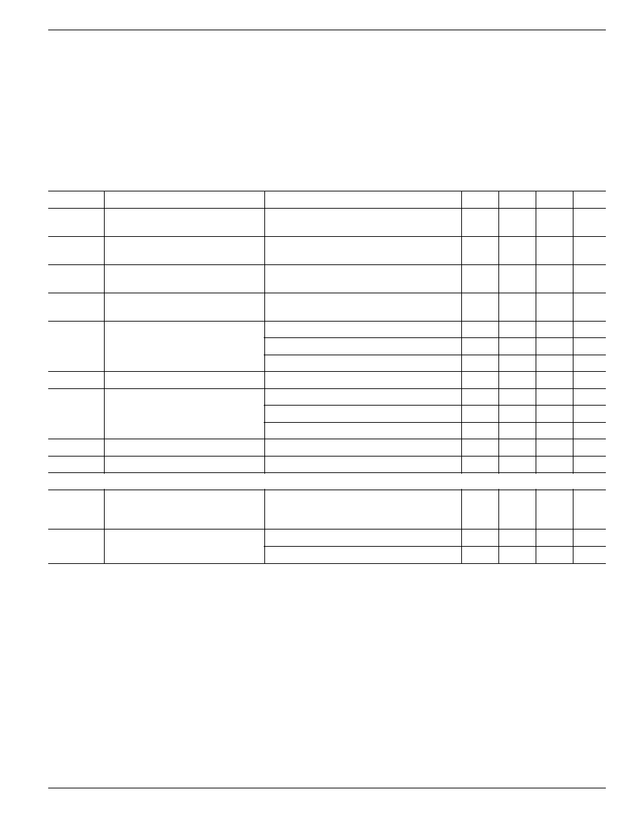
Electrical Characteristics
V
IN
= V
OUT
+ 1V; I
L
= 1mA; C
L
= 0.1
µ
F, and V
EN
2.0V; T
J
= 25
∞
C, bold values indicate ≠40
∞
C to +125
∞
C;
for one-half of dual MIC5211; unless noted.
Symbol
Parameter
Conditions
Min
Typical
Max
Units
V
O
Output Voltage
variation from nominal V
OUT
≠3
3
%
Accuracy
≠4
4
%
V
O
/
T
Output Voltage
Note 5
50
200
ppm/
∞
C
Temperature Coeffcient
V
O
/V
O
Line Regulation
V
IN
= V
OUT
+1V to 16V
0.008
0.3
%
0.5
%
V
O
/V
O
Load Regulation
I
L
= 0.1mA to 50mA, Note 6
0.08
0.3
%
0.5
%
V
IN
≠ V
O
Dropout Voltage, Note 7
I
L
= 100
µ
A
20
mV
I
L
= 20mA
200
450
mV
I
L
= 50mA
250
500
mV
I
Q
Quiescent Current
V
EN
0.4V (shutdown)
0.01
10
µ
A
I
GND
Ground Pin Current
V
EN
2.0V, I
L
= 100
µ
A (active)
90
µ
A
Note 8
I
L
= 20mA (active)
225
450
µ
A
I
L
= 50mA (active)
750
1200
µ
A
I
LIMIT
Current Limit
V
OUT
= 0V
140
250
mA
V
O
/
P
D
Thermal Regulation
Note 9
0.05
%/W
Enable Input
Enable Input Voltage Level
V
IL
logic low (off)
0.6
V
V
IH
logic high (on)
2.0
V
I
IL
Enable Input Current
V
IL
0.6V
0.01
1
µ
A
I
IH
V
IH
2.0V
3
50
µ
A
Note 1:
Exceeding the absolute maximum rating may damage the device.
Note 2:
The device is not guareented to function outside itsperating rating.
Note 3:
Devices are ESD sensitive. Handling precautions recommended.
Note 4:
The maximum allowable power dissipation at any T
A
(ambient temperature) is P
D(max)
= (T
J(max)
≠ T
A
) /
JA
. Exceeding the maximum
allowable power dissipation will result in excessive die temperature, and the regulator will go into thermal shutdown. The
JA
is 220
∞
C/W for
the SOT-23-6 mounted on a printed circuit board.
Note 5:
Output voltage temperature coeffiecient is defined as the worst case voltage change divided by the total temperature range.
Note 6:
Regulation is measured at constant junction temperature using low duty cycle pulse testing. Parts are tested for load regulation in the load
range from 0.1mA to 50mA. Change in output voltage due to heating effects are covered by thermal regulation specification.
Note 7:
Dropout voltage is defined as the input to output differential at which the output voltage drops 2% below its nominal value measured at 1V
differential. For output voltages below 2.5V, dropout voltage is the input-to-output voltage differential with the minimum voltage being 2.5V.
Minimum input opertating voltage is 2.5V.
Note 8:
Ground pin current is the quiescent current per regulator plus pass transistor base current. The total current drawn from the supply is the sum
of the load current plus the ground pin current.
Note 9:
Thermal regulation is defined as the change in output voltage at a time "t" after a change in power dissipation is applied, excluding load or line
regulation effects. Specifications are for a 50mA load pulse at V
IN
= 16V for t = 10ms.
Operating Ratings (Note 2)
Supply Input Voltage (V
IN
) ............................... 2.5V to 16V
Enable Input Voltage (V
EN
) ................................. 0V to 16V
Junction Temperature (T
J
) (except 1.8V) . ≠40
∞
C to +125
∞
C
1.8V only .................................................. 0
∞
C to +125
∞
C
6-lead SOT-23-6
(
JA
) .............................................. Note 4


