April 2003
1
MIC5212
MIC5212
Micrel
MIC5212
Dual 500mA LDO Regulator
Final
General Description
The MIC5212 is a dual linear voltage regulator with very-low
dropout voltage (typically 10mV at light loads and 350mV at
500mA), very-low ground current (225
µ
A at 10mA output),
and better than 1% initial accuracy.
Both regulator outputs can supply up to 500mA at the same
time as long as each regulator's maximum junction tempera-
ture is not exceeded.
Key features include current limiting, overtemperature shut-
down, and protection against reversed battery.
The MIC5212 is available in a fixed 3.3V/2.5V output voltage
configuration. Other voltages are available; contact Micrel for
details.
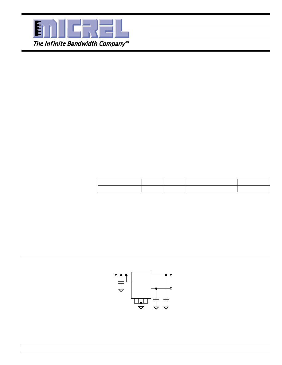
Typical Application
V
O1
= 3.3V
V
O2
= 2.5V
IN = 5V
4.7
µ
F
4.7
µ
F 4.7
µ
F
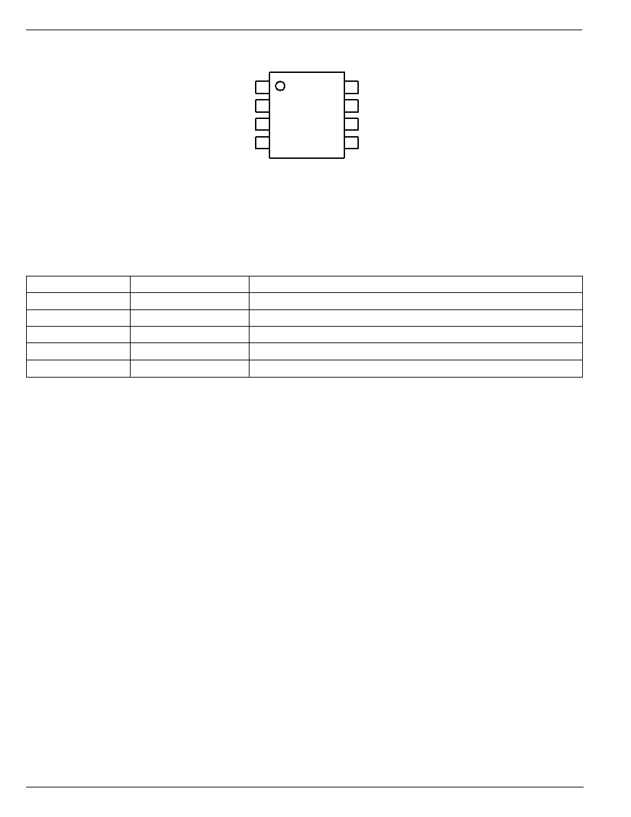
MIC5212-SJBM
GND
OUTB
OUTA
INA
INB
3.3V/2.5V Dual LDO
Features
∑ Fused lead frame SOIC-8
∑ Up to 500mA per regulator output
∑ Low quiescent current
∑ Low dropout voltage
∑ Tight load and line regulation
∑ Low temperature coefficient
∑ Current and thermal limiting
∑ Reversed input polarity protection
Applications
∑ Hard disk drives
∑ CD R/W
∑ Bar code scanners
∑ SMPS post regulator/DC-to-DC modules
∑ High-efficiency linear power supplies
Micrel, Inc. ∑ 1849 Fortune Drive ∑ San Jose, CA 95131 ∑ USA ∑ tel + 1 (408) 944-0800 ∑ fax + 1 (408) 944-0970 ∑ http://www.micrel.com
Ordering Information
Part Number
Voltage
Accuracy
Junction Temp. Range*
Package
MIC5212-SJBM
3.3V/2.5V
1.0%
≠40
∞
C to +125
∞
C
8-lead SOIC
Other voltages available. Contact Micrel for details.

April 2003
3
MIC5212
MIC5212
Micrel
Electrical Characteristics
Regulator A and B V
IN
= V
OUT
+ 1V; I
L
= 100
µ
A; C
L
= 4.7
µ
F; T
J
= 25
∞
C, bold values indicate ≠40
∞
C
T
J
+125
∞
C; unless noted.
Symbol
Parameter
Conditions
Min
Typical
Max
Units
V
O
Output Voltage Accuracy
variation from specified V
OUT
≠1
1
%
≠2
2
%
V
O
/
T
Output Voltage
Note 4
40
ppm/
∞
C
Temperature Coefficient
V
O
/V
O
Line Regulation
V
IN
= V
OUT
+ 1V to 16V
0.009
0.05
% / V
0.1
% / V
V
O
/V
O
Load Regulation
I
L
= 0.1mA to 500mA, Note 5
0.05
0.7
%
1.0
%
V
IN
≠ V
O
Dropout Voltage, Note 6
I
L
= 150mA
175
275
mV
(per regulator)
350
mV
I
L
= 500mA
350
500
mV
600
mV
I
GND
Ground Pin Current, Note 7
I
L
= 150mA
1.5
2.5
mA
(per regulator)
3.0
mA
I
L
= 500mA
12
20
mA
25
mA
PSRR
Ripple Rejection
f = 120Hz, I
L
= 150mA
75
dB5
I
LIMIT
Current Limit
V
OUT
= 0V
750
1000
mA
Spectral Noise Density
V
OUT
= 2.5V, I
OUT
= 50mA, C
OUT
= 2.2
µ
F
500
nV/
Hz
Note 1.
Exceeding the absolute maximum rating may damage the device.
Note 2.
The device is not guaranteed to function outside its operating rating.
Note 3.
Absolute maximum ratings indicate limits beyond which damage to the component may occur. Electrical specifications do not apply when
operating the device outside of its operating ratings. The maximum allowable power dissipation is a function of the maximum junction
temperature, T
J(max)
, the junction-to-ambient thermal resistance,
JA
, and the ambient temperature, T
A
. The maximum allowable power
dissipation at any ambient temperature is calculated using: P
D(max)
= (T
J(max)
≠ T
A
)
˜
JA
. Exceeding the maximum allowable power dissipa-
tion will result in excessive die temperature, and the regulator will go into thermal shutdown. The
JA
of the 8-lead SOIC (M) is 63
∞
C/W
mounted on a PC board (see
"Thermal Considerations"
section for further details).
Note 4.
Output voltage temperature coefficient is defined as the worst case voltage change divided by the total temperature range.
Note 5.
Regulation is measured at constant junction temperature using low duty cycle pulse testing. Parts are tested for load regulation in the load
range from 0.1mA to 500mA. Changes in output voltage due to heating effects are covered by the thermal regulation specification.
Note 6.
Dropout voltage is defined as the input to output differential at which the output voltage drops 2% below its nominal value measured at 1V
differential.
Note 7.
Ground pin current is the regulator quiescent current plus pass transistor base current. The total current drawn from the supply is the sum of
the load current plus the ground pin current.
Absolute Maximum Ratings
(Note 1)
Supply Input Voltage (V
IN
A or B) ................. ≠20V to +20V
Power Dissipation (P
D
) ............................ Internally Limited
Storage Temperature Range ................... ≠60
∞
C to +150
∞
C
Lead Temperature (soldering, 5 sec.) ....................... 260
∞
C
Operating Ratings
(Note 2)
Supply Input Voltage (V
IN
) ............................... 2.5V to 16V
Junction Temperature (T
J
) ....................... ≠40
∞
C to +125
∞
C
Thermal Resistance
(
JA
) ......................................... Note 3