September 2002
1
MIC5213
MIC5213
Micrel
General Description
The MIC5213 is a
µ
Cap 80mA linear voltage regulator in the
TeenyTM SC-70 package. Featuring half the footprint of the
standard SOT-23 package, this TeenyTM SC-70 regulator
has very low dropout voltage (typically 20mV at light loads
and 300mV at 80mA) and very low ground current (225
µ
A at
20mA output). It also offers better than 3% initial accuracy
and includes a logic-compatible enable input.
The
µ
Cap regulator design is optimized to work with low-
value, low-cost ceramic capacitors. The outputs typically
require only 0.47
µ
F of output capacitance for stability.
Designed especially for hand-held, battery-powered devices,
the MIC5213 can be controlled by a CMOS or TTL compatible
logic signal. When disabled, power consumption drops nearly
to zero. If on-off control is not required, the enable pin may be
tied to the input for 3-terminal operation. The ground current
of the MIC5213 increases only slightly in dropout, further
prolonging battery life. Key MIC5213 features include current
limiting, overtemperature shutdown, and protection against
reversed battery.
The MIC5213 is available in 2.5V, 2.6V, 2.7V, 2.8V, 3.0V,
3.3V, 3.6V, and 5.0V fixed voltages. Other voltages are
available; contact Micrel for details.
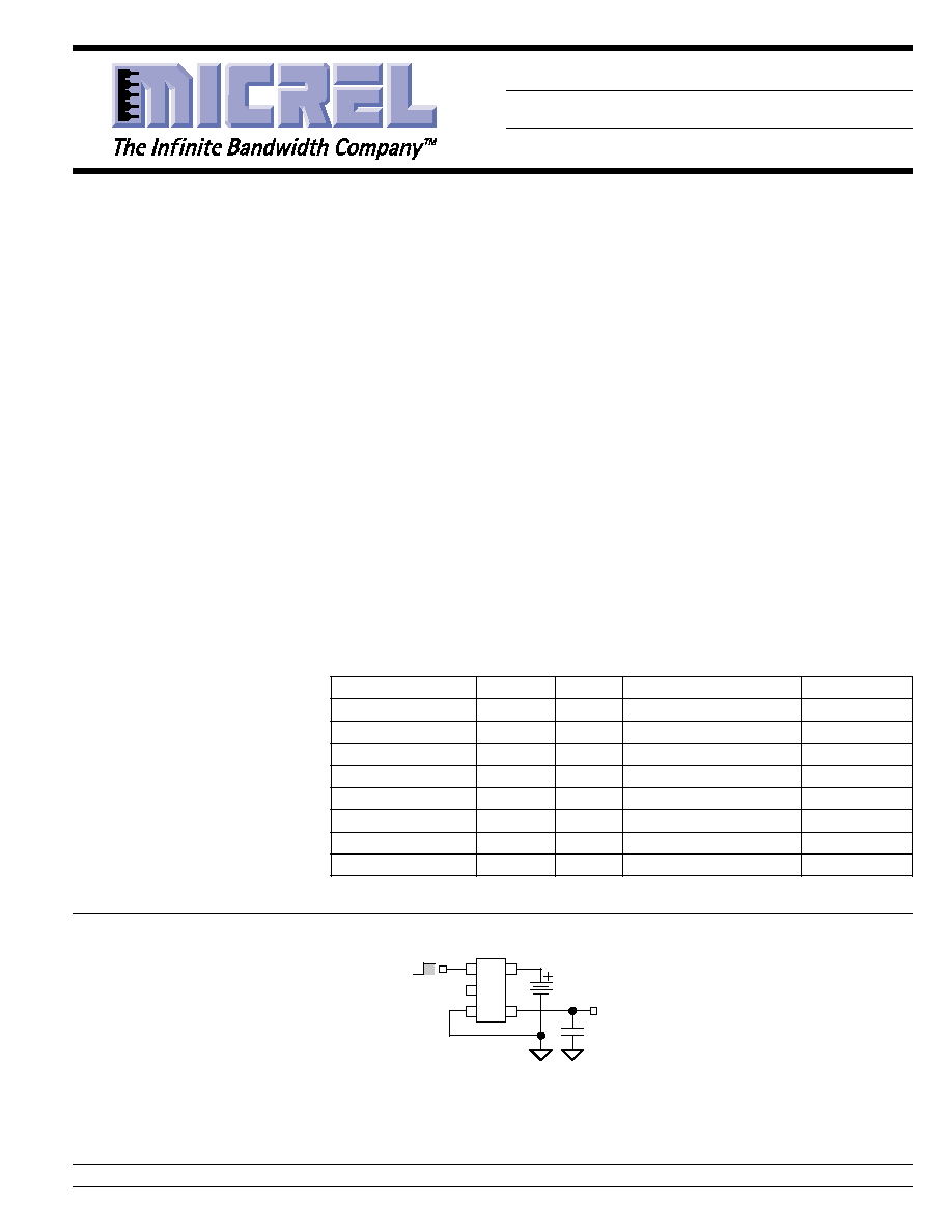
Typical Applications
1
5
2
3
4
0.47µF
V
OUT
Enable
Shutdown
LAx
Regulator Circuit
Ordering Information
Part Number
Marking
Voltage
Junction Temp. Range
Package
MIC5213-2.5BC5
LAM
2.5V
≠40
∞
C to +125
∞
C
SC-70-5
MIC5213-2.6BC5
LAQ
2.6V
≠40
∞
C to +125
∞
C
SC-70-5
MIC5213-2.7BC5
LAL
2.7V
≠40
∞
C to +125
∞
C
SC-70-5
MIC5213-2.8BC5
LAJ
2.8V
≠40
∞
C to +125
∞
C
SC-70-5
MIC5213-3.0BC5
LAG
3.0V
≠40
∞
C to +125
∞
C
SC-70-5
MIC5213-3.3BC5
LAE
3.3V
≠40
∞
C to +125
∞
C
SC-70-5
MIC5213-3.6BC5
LAD
3.6V
≠40
∞
C to +125
∞
C
SC-70-5
MIC5213-5.0BC5
LAB
5.0V
≠40
∞
C to +125
∞
C
SC-70-5
Other voltages available. Contact Micrel for details.
Features
∑ TeenyTM SC-70 package
∑ Wide selection of output voltages
∑ Guaranteed 80mA output
∑ Low quiescent current
∑ Low dropout voltage
∑ Tight load and line regulation
∑ Low temperature coefficient
∑ Current and thermal limiting
∑ Reversed input polarity protection
∑ Zero off-mode current
∑ Logic-controlled shutdown
∑ Stability with low ESR ceramic capacitors
Applications
∑ Cellular telephones
∑ Laptop, notebook, and palmtop computers
∑ Battery-powered equipment
∑ Bar code scanners
∑ SMPS post-regulator/dc-to-dc modules
∑ High-efficiency linear power supplies
MIC5213
TeenyTM SC-70
µ
Cap Low-Dropout Regulator
Final Information
Teeny is a trademark of Micrel, Inc.
Micrel, Inc. ∑ 1849 Fortune Drive ∑ San Jose, CA 95131 ∑ USA ∑ tel + 1 (408) 944-0800 ∑ fax + 1 (408) 944-0970 ∑ http://www.micrel.com
MIC5213
2
September 2002
MIC5213
Micrel
Absolute Maximum Ratings
(Note 1)
Input Supply Voltage (V
IN
) ............................ ≠20V to +20V
Enable Input Voltage (V
EN
) ........................... ≠20V to +20V
Power Dissipation (P
D
) ............................ Internally Limited
Storage Temperature Range (T
S
) ............ ≠60
∞
C to +150
∞
C
Lead Temperature (Soldering, 5 sec.) ...................... 260
∞
C
ESD, Note 3
Operating Ratings
(Note 2)
Input Voltage (V
IN
) ........................................... 2.5V to 16V
Enable Input Voltage (V
EN
) .................................. 0V to V
IN
Junction Temperature Range ................... ≠40
∞
C to +125
∞
C
Thermal Resistance
(
JA
) ......................................... Note 4
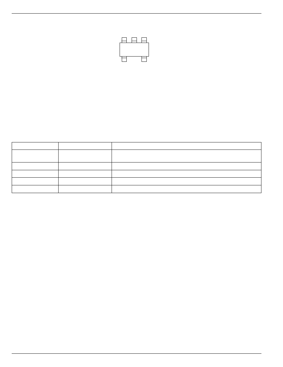
Pin Configuration
EN
IN
OUT
GND
LAx
1
3
4
5
2
NC
SC-70-5 (C5)
Pin Description
Pin Number
Pin Name
Pin Function
1
EN
Enable (Input): TTL/CMOS compatible control input. Logic high = enabled;
logic low or open = shutdown.
2
NC
Not internally connected.
3
GND
Ground
4
OUT
Regulator Output
5
IN
Supply Input
September 2002
3
MIC5213
MIC5213
Micrel
Electrical Characteristics
V
IN
= V
OUT
+ 1V; I
L
= 1mA; C
L
= 0.47
µ
F; V
EN
2.0V; T
J
= 25
∞
C, bold values indicate ≠40
∞
C
T
J
+125
∞
C; unless noted.
Symbol
Parameter
Conditions
Min
Typ
Max
Units
V
O
Output Voltage Accuracy
≠3
3
%
≠4
4
%
V
O
/
T
Output Voltage Temp. Coefficient
Note 5
50
200
ppm/
∞
C
V
O
/V
O
Line Regulation
V
IN
= V
OUT
+ 1V to 16V
0.008
0.3
%
0.5
%
V
O
/V
O
Load Regulation
I
L
= 0.1mA to 80mA, Note 6
0.08
0.3
%
0.5
%
V
IN
≠V
O
Dropout Voltage, Note 7
I
L
= 100
µ
A
20
mV
I
L
= 20mA
200
350
mV
I
L
= 50mA
250
mV
I
L
= 80mA
280
600
mV
I
Q
Quiescent Current
V
EN
0.4V (shutdown)
0.01
10
µ
A
I
GND
Ground Pin Current, Note 8
I
L
= 100
µ
A, V
EN
2.0V (active)
180
µ
A
I
L
= 20mA, V
EN
2.0V (active)
225
750
µ
A
I
L
= 50mA, V
EN
2.0V (active)
850
µ
A
I
L
= 80mA, V
EN
2.0V (active)
1800
3000
µ
A
I
GNDDO
Ground Pin Current in Dropout
V
IN
= V
OUT(nominal)
≠ 0.5V, Note 8
200
300
µ
A
I
LIMIT
Current Limit
V
OUT
= 0V
180
250
mA
V
O/
P
D
Thermal Regulation
Note 9
0.05
%/W
Enable Input
V
IL
Enable Input Voltage Level
Logic Low (off)
0.6
V
V
IH
Logic High (on)
2.0
V
I
IL
Enable Input Current
V
IL
0.6V
0.01
1
µ
A
I
IH
V
IH
2.0V
8
50
µ
A
Note 1.
Exceeding the absolute maximum rating may damage the device.
Note 2.
The device is not guaranteed to function outside its operating rating.
Note 3.
Devices are ESD sensitive. Handling precautions recommended.
Note 4.
The maximum allowable power dissipation is a function of the maximum junction temperature, T
J(max)
, the junction-to-ambient thermal
resistance,
JA
, and the ambient temperature, T
A
. The maximum allowable power dissipation at any ambient temperature is calculated using:
P
D(max)
= (T
J(max)
≠ T
A
)
˜
JA
. Exceeding the maximum allowable power dissipation will result in excessive die temperature, and the regulator
will go into thermal shutdown.
JA
of the SC-70-5 is 450
∞
C/W, mounted on a PC board.
Note 5.
Output voltage temperature coefficient is defined as the worst case voltage change divided by the total temperature range.
Note 6.
Regulation is measured at constant junction temperature using low duty cycle pulse testing. Changes in output voltage due to heating effects
are covered by the thermal regulation specification.
Note 7.
Dropout voltage is defined as the input to output differential at which the output voltage drops 2% below its nominal value measured at 1V
differential.
Note 8.
Ground pin current is the regulator quiescent current plus pass transistor base current. The total current drawn from the supply is the sum of
the load current plus the ground pin current.
Note 9.
Thermal regulation is defined as the change in output voltage at a time "t" after a change in power dissipation is applied, excluding load or line
regulation effects. Specifications are for an 80mA load pulse at V
IN
= 16V for t = 10ms.

MIC5213
4
September 2002
MIC5213
Micrel
1
10
100
1000
0.01
0.1
1
10
100
DROPOUT VOLTAGE (mV)
OUTPUT CURRENT (mA)
Dropout Voltage
vs. Output Current
C
IN
= 10
µ
F
C
OUT
= 1
µ
F
0
100
200
300
400
-60 -30
0
30
60
90 120 150
DROPOUT VOLTAGE (mV)
TEMPERATURE (
∞
C)
Dropout Voltage
vs. Temperature
C
IN
= 10
µ
F
C
OUT
= 1
µ
F
I
L
= 100
µ
A
I
L
= 1mA
I
L
= 80mA
0
1
2
3
4
0
1
2
3
4
5
6
7
OUTPUT VOLTAGE (V)
SUPPLY VOLTAGE (V)
Dropout
Characteristics
I
L
= 80mA
I
L
= 100
µ
A
C
IN
= 10
µ
F
C
OUT
= 1
µ
F
0
500
1000
1500
2000
0
10 20 30 40 50 60 70 80
GROUND CURRENT (
µ
A)
OUTPUT CURRENT (mA)
Ground Current
vs. Output Current
V
IN
= V
OUT
+ 1V
0.0
0.5
1.0
1.5
2.0
0
1
2
3
4
5
6
7
GROUND CURRENT (mA)
SUPPLY VOLTAGE (V)
Ground Current
vs. Supply Voltage
I
L
= 50mA
I
L
= 100
µ
A
V
OUT
= 3.3V
0.0
0.5
1.0
1.5
2.0
2.5
3.0
-60 -30
0
30
60
90 120 150
GROUND CURRENT (mA)
TEMPERATURE (
∞
C)
Ground Current
vs. Temperature
I
L
= 50mA
I
L
= 100
µ
A
C
IN
= 10
µ
F
C
OUT
= 1
µ
F
I
L
= 80mA
Typical Characteristics
0.0
0.5
1.0
1.5
2.0
2.5
3.0
3.5
4.0
0
50
100
150
200
OUTPUT VOLTAGE (V)
OUTPUT CURRENT (mA)
C
IN
= 10
µ
F
C
OUT
= 1
µ
F
Output Voltage
vs. Output Current
0
20
40
60
80
100
120
140
160
0
1
2
3
4
5
6
7
SHORT CIRCUIT CURRENT (mA)
INPUT VOLTAGE (V)
Short Circuit Current
vs. Input Voltage
C
IN
= 10
µ
F
C
OUT
= 1
µ
F
-60
-40
-20
0
20
40
60
OUTPUT (mV)
-50
0
50
100
-2
0
2
4
6
8 10 12 14 16
LOAD (mA)
TIME (ms)
Thermal Regulation
(3.3V Version)
C
L
= 1
µ
F
2.4
2.6
2.8
3.0
3.2
3.4
3.6
3.8
4.0
-60 -30
0
30
60
90 120 150
OUTPUT VOLTAGE (V)
TEMPERATURE (
∞
C)
Output Voltage
vs. Temperature
C
IN
= 10
µ
F
C
OUT
= 1
µ
F
CURVES APPLICABLE
AT 100
µ
A AND 50mA
3 DEVICES
HI / AVG / LO
100
120
140
160
180
200
-60 -30
0
30
60
90 120 150
OUTPUT CURRENT (mA)
TEMPERATURE (
∞
C)
Short Circuit Current
vs. Temperature
C
IN
= 10
µ
F
C
OUT
= 1
µ
F
3.3
3.4
3.5
-60 -30
0
30
60
90 120 150
MIN. SUPPLY VOLTAGE (V)
TEMPERATURE (
∞
C)
Minimum Supply Voltage
vs. Temperature
I
L
= 1mA
V
OUT
= 3.3V
C
IN
= 10
µ
F
C
OUT
= 1
µ
F

September 2002
5
MIC5213
MIC5213
Micrel
OUTPUT (mV)
-50
0
50
100
-1
0
1
2
3
4
5
6
7
8
OUTPUT (mA)
TIME (ms)
Load Transient
C
OUT
= 1
µ
F
V
IN
= V
OUT
+ 1
0
40
-40
-50
0
50
100
-5
0
5
10
15
20
OUTPUT (mA)
TIME (ms)
-200
-100
0
100
OUTPUT (mV)
Load Transient
C
OUT
= 10
µ
F
V
IN
= V
OUT
+ 1
-2
-1
0
1
2
3
OUTPUT (V)
2
4
6
8
-0.2
0.0
0.2
0.4
0.6
0.8
1.0
INPUT (V)
TIME (ms)
Line Transient
C
L
= 1
µ
F
I
L
= 1mA
-1
0
1
2
OUTPUT (V)
2
4
6
8
-0.2
0.0
0.2
0.4
0.6
0.8
1.0
INPUT (V)
TIME (ms)
Line Transient
C
L
= 11
µ
F
I
L
= 1mA
0
20
40
60
80
100
10x10
0
100x10
0
1x10
3
10x10
3
100x10
3
1x10
6
RIPPLE VOLTAGE (dB)
FREQUENCY (Hz)
Ripple Voltage
vs. Frequency
I
L
= 1mA
C
L
= 1
µ
F
V
IN
= V
OUT
+ 1
0
20
40
60
80
100
10x10
0
100x10
0
1x10
3
10x10
3
100x10
3
1x10
6
RIPPLE VOLTAGE (dB)
FREQUENCY (Hz)
Ripple Voltage
vs. Frequency
I
L
= 50mA
C
L
= 1
µ
F
V
IN
= V
OUT
+ 1
0
20
40
60
80
100
10x10
0
100x10
0
1x10
3
10x10
3
100x10
3
1x10
6
RIPPLE VOLTAGE (dB)
FREQUENCY (Hz)
Ripple Voltage
vs. Frequency
I
L
= 100
µ
A
C
L
= 1
µ
F
V
IN
= V
OUT
+ 1