
November 2002
1
MIC5219
MIC5219
Micrel
Typical Applications
MIC5219
500mA-Peak Output LDO Regulator
Final
General Description
The MIC5219 is an efficient linear voltage regulator with high
peak output current capability, very low dropout voltage, and
better than 1% output voltage accuracy. Dropout is typically
10mV at light loads and less than 500mV at full load.
The MIC5219 is designed to provide a peak output current for
startup conditions where higher inrush current is demanded.
It features a 500mA peak output rating. Continuous output
current is limited only by package and layout.
The MIC5219 can be enabled or shut down by a CMOS or
TTL compatible signal. When disabled, power consumption
drops nearly to zero. Dropout ground current is minimized to
help prolong battery life. Other key features include reversed-
battery protection, current limiting, overtemperature shut-
down, and low noise performance with an ultra-low-noise
option.
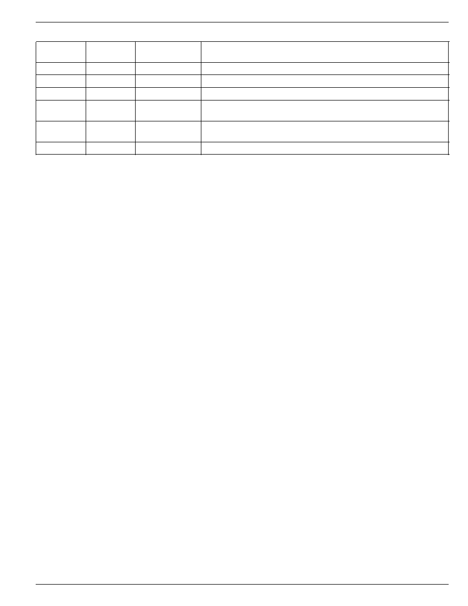
The MIC5219 is available in adjustable or fixed output volt-
ages in space-saving SOT-23-5 and MM8TM 8-lead power
MSOP packages. For higher power requirements see the
MIC5209 or MIC5237.
Features
∑ 500mA Output current capability
∑ SOT-23-5 package - 500mA peak
∑ MSOP-8 package - 500mA continuous
∑ Low 500mV maximum dropout voltage at full load
∑ Extremely tight load and line regulation
∑ Tiny SOT-23-5 and MM8TM power MSOP-8 package
∑ Ultra-low-noise output
∑ Low temperature coefficient
∑ Current and thermal limiting
∑ Reversed-battery protection
∑ CMOS/TTL-compatible enable/shutdown control
∑ Near-zero shutdown current
Applications
∑ Laptop, notebook, and palmtop computers
∑ Cellular telephones and battery-powered equipment
∑ Consumer and personal electronics
∑ PC Card V
CC
and V
PP
regulation and switching
∑ SMPS post-regulator/dc-to-dc modules
∑ High-efficiency linear power supplies
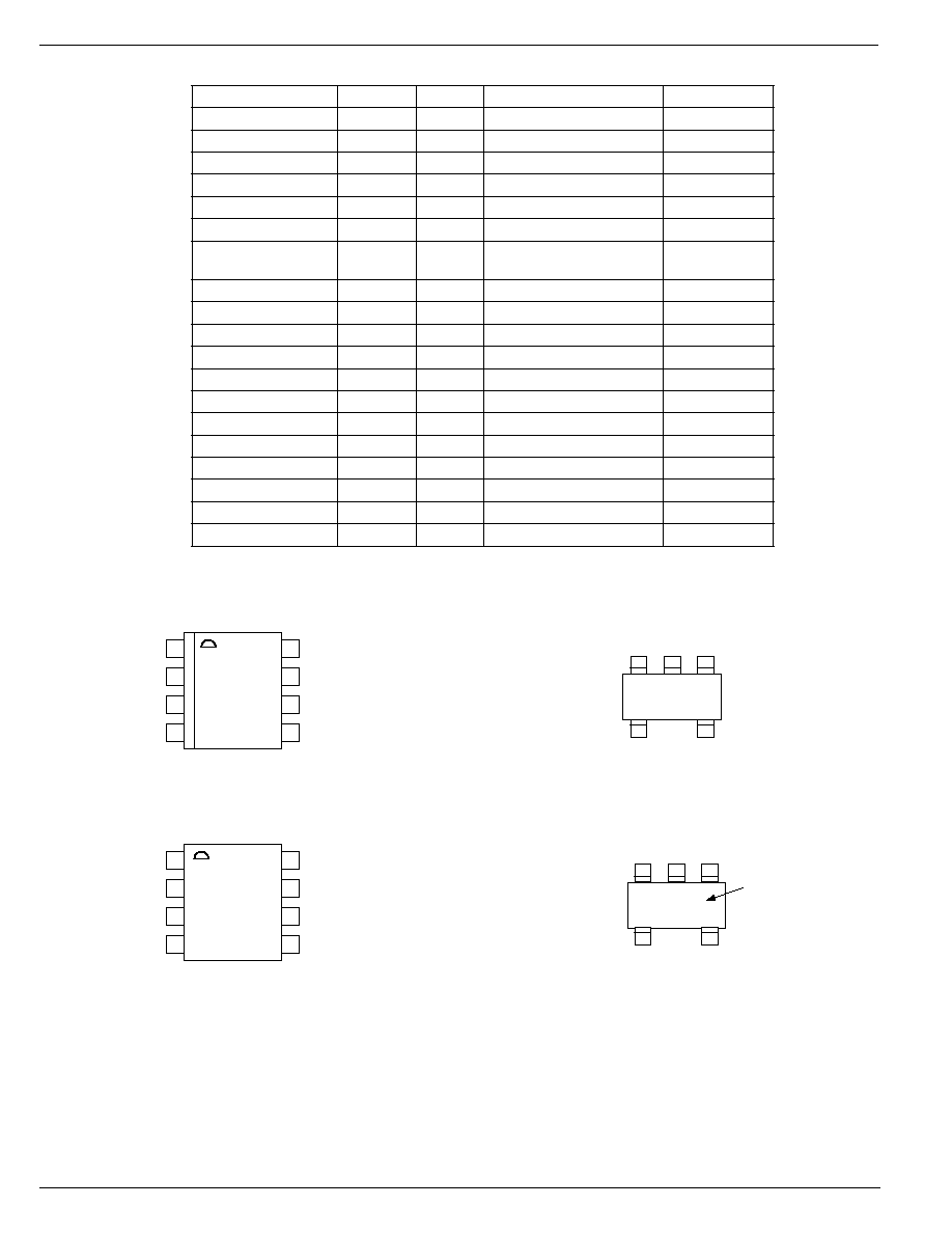
1
2
3
4
8
7
6
5
MIC5219-5.0BMM
2.2µF
tantalum
V
OUT
5V
V
IN
6V
ENABLE
SHUTDOWN
470pF
5V Ultra-Low-Noise Regulator
1
5
2
3
4
2.2µF
tantalum
470pF
V
OUT
3.3V
MIC5219-3.3BM5
V
IN
4V
ENABLE
SHUTDOWN
3.3V Ultra-Low-Noise Regulator
Micrel, Inc. ∑ 1849 Fortune Drive ∑ San Jose, CA 95131 ∑ USA ∑ tel + 1 (408) 944-0800 ∑ fax + 1 (408) 944-0970 ∑ http://www.micrel.com
MM8 is a trademark of Micrel, Inc.
MIC5219
Micrel
MIC5219
2
November 2002
Ordering Information
Part Number
Marking
Volts
Junction Temp. Range
Package
MIC5219-2.85BMM
--
2.85V
≠40
∞
C to +125
∞
C
MSOP-8
MIC5219-3.0BMM
--
3.0V
≠40
∞
C to +125
∞
C
MSOP-8
MIC5219-3.3BMM
--
3.3V
≠40
∞
C to +125
∞
C
MSOP-8
MIC5219-3.6BMM
--
3.6V
≠40
∞
C to +125
∞
C
MSOP-8
MIC5219-5.0BMM
--
5.0V
≠40
∞
C to +125
∞
C
MSOP-8
MIC5219BMM
--
Adj.
≠40
∞
C to +125
∞
C
MSOP-8
MIC5219YMM
--
Adj.
≠40
∞
C to +125
∞
C
MSOP-8
Lead-Free
MIC5219-2.5BM5
LG25
2.5V
≠40
∞
C to +125
∞
C
SOT-23-5
MIC5219-2.6BM5
LG26
2.6V
≠40
∞
C to +125
∞
C
SOT-23-5
MIC5219-2.7BM5
LG27
2.7V
≠40
∞
C to +125
∞
C
SOT-23-5
MIC5219-2.8BM5
LG28
2.8V
≠40
∞
C to +125
∞
C
SOT-23-5
MIC5219-2.85BM5
LG2J
2.85V
≠40
∞
C to +125
∞
C
SOT-23-5
MIC5219-2.9BM5
LG29
2.9V
≠40
∞
C to +125
∞
C
SOT-23-5
MIC5219-3.1BM5
LG31
3.1V
≠40
∞
C to +125
∞
C
SOT-23-5
MIC5219-3.0BM5
LG30
3.0V
≠40
∞
C to +125
∞
C
SOT-23-5
MIC5219-3.3BM5
LG33
3.3V
≠40
∞
C to +125
∞
C
SOT-23-5
MIC5219-3.6BM5
LG36
3.6V
≠40
∞
C to +125
∞
C
SOT-23-5
MIC5219-5.0BM5
LG50
5.0V
≠40
∞
C to +125
∞
C
SOT-23-5
MIC5219BM5
LGAA
Adj.
≠40
∞
C to +125
∞
C
SOT-23-5
Other voltages available. Consult Micrel for details.
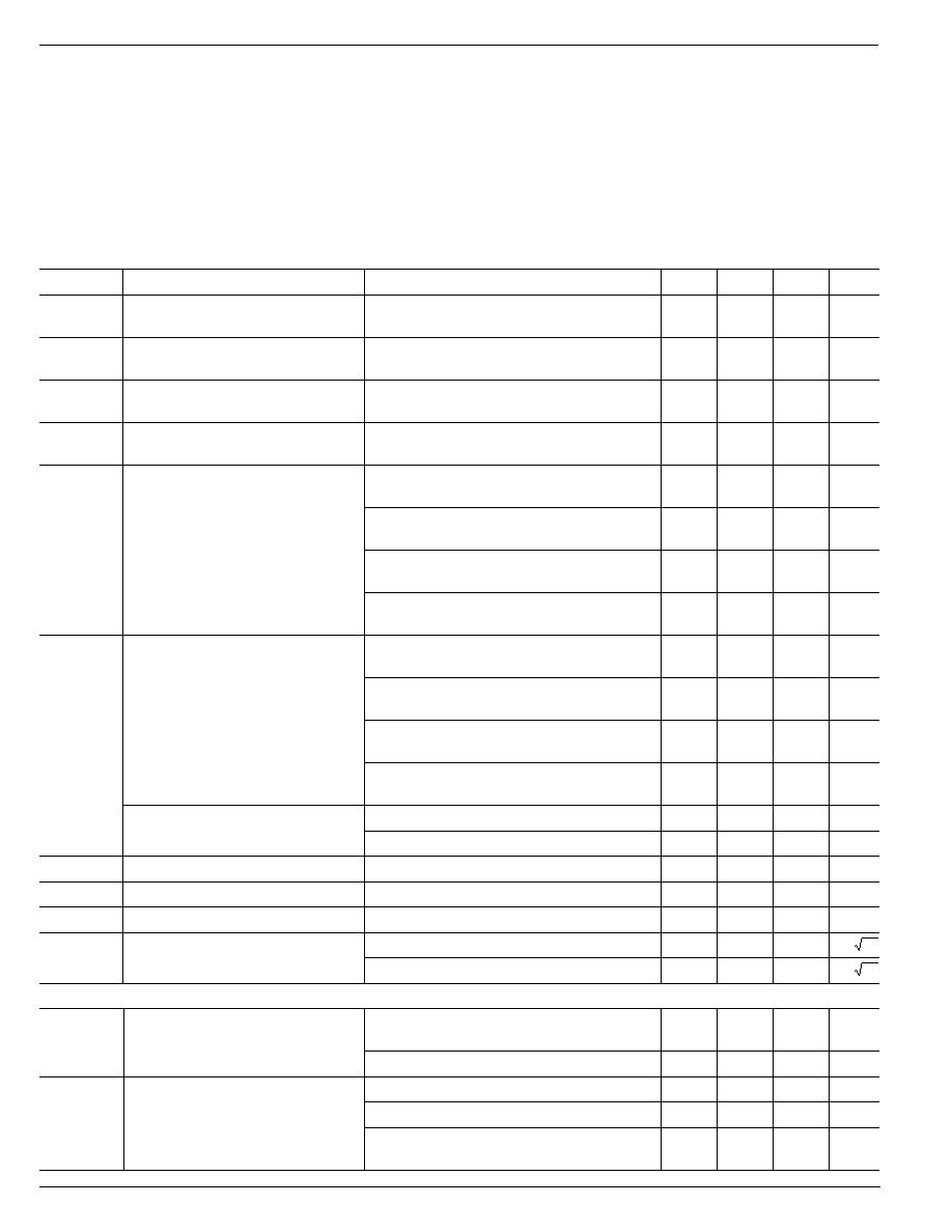
1
2
3
4
8
7
6
5
GND
GND
GND
GND
EN
IN
OUT
BYP
MIC5219-x.xBMM
MM8TM MSOP-8
Fixed Voltages
1
2
3
4
8
7
6
5
GND
GND
GND
GND
EN
IN
OUT
ADJ
MIC5219YMM
MIC5219BMM
MM8TM MSOP-8
Adjustable Voltage
IN
OUT
BYP
EN
LGxx
1
3
4
5
2
GND
MIC5219-x.xBM5
SOT-23-5
Fixed Voltages
Part
Identification
IN
OUT
ADJ
EN
LGAA
1
3
4
5
2
GND
MIC5219BM5
SOT-23-5
Adjustable Voltage
Pin Configuration
November 2002
3
MIC5219
MIC5219
Micrel
Pin Description
Pin No.
Pin No.
Pin Name
Pin Function
MSOP-8
SOT-23-5
2
1
IN
Supply Input
5≠8
2
GND
Ground: MSOP-8 pins 5 through 8 are internally connected.
3
5
OUT
Regulator Output
1
3
EN
Enable (Input): CMOS compatible control input. Logic high = enable; logic
low or open = shutdown.
4 (fixed)
4 (fixed)
BYP
Reference Bypass: Connect external 470pF capacitor to GND to reduce
output noise. May be left open.
4 (adj.)
4 (adj.)
ADJ
Adjust (Input): Feedback input. Connect to resistive voltage-divider network.
MIC5219
Micrel
MIC5219
4
November 2002
Electrical Characteristics
V
IN
= V
OUT
+ 1.0V; C
OUT
= 4.7
µ
F, I
OUT
= 100
µ
A; T
J
= 25
∞
C, bold values indicate ≠40
∞
C
T
J
+125
∞
C; unless noted.
Symbol
Parameter
Conditions
Min
Typical
Max
Units
V
OUT
Output Voltage Accuracy
variation from nominal V
OUT
≠1
1
%
≠2
2
%
V
OUT
/
T
Output Voltage
Note 2
40
ppm/
∞
C
Temperature Coefficient
V
OUT
/V
OUT
Line Regulation
V
IN
= V
OUT
+ 1V to 12V
0.009
0.05
%/V
0.1
V
OUT
/V
OUT
Load Regulation
I
OUT
= 100
µ
A to 500mA Note 3
0.05
0.5
%
0.7
V
IN
≠ V
OUT
Dropout Voltage, Note 4
I
OUT
= 100
µ
A
10
60
mV
80
I
OUT
= 50mA
115
175
mV
250
I
OUT
= 150mA
175
300
mV
400
I
OUT
= 500mA
350
500
mV
600
I
GND
Ground Pin Current, Notes 5, 6
V
EN
3.0V, I
OUT
= 100
µ
A
80
130
µ
A
170
V
EN
3.0V, I
OUT
= 50mA
350
650
µ
A
900
V
EN
3.0V, I
OUT
= 150mA
1.8
2.5
mA
3.0
V
EN
3.0V, I
OUT
= 500mA
12
20
mA
25
Ground Pin Quiescent Current,
V
EN
0.4V
0.05
3
µ
A
Note 6
V
EN
0.18V
0.10
8
µ
A
PSRR
Ripple Rejection
f = 120Hz
75
dB
I
LIMIT
Current Limit
V
OUT
= 0V
700
1000
mA
V
OUT
/
P
D
Thermal Regulation
Note 7
0.05
%/W
e
no
Output Noise
I
OUT
= 50mA, C
OUT
= 2.2
µ
F, C
BYP
= 0
500
nV/ Hz
I
OUT
= 50mA, C
OUT
= 2.2
µ
F, C
BYP
= 470pF
300
nV/ Hz
ENABLE Input
V
ENL
Enable Input Logic-Low Voltage
V
EN
= logic low (regulator shutdown)
0.4
V
0.18
V
EN
= logic high (regulator enabled)
2.0
V
I
ENL
Enable Input Current
V
ENL
0.4V
0.01
≠1
µ
A
V
ENL
0.18V
0.01
≠2
µ
A
I
ENH
V
ENH
2.0V
2
5
20
µ
A
25
Absolute Maximum Ratings
Supply Input Voltage (V
IN
) ............................ ≠20V to +20V
Power Dissipation (P
D
) ............................ Internally Limited
Junction Temperature (T
J
) ....................... ≠40
∞
C to +125
∞
C
Storage Temperature (T
S
) ....................... ≠65
∞
C to +150
∞
C
Lead Temperature (Soldering, 5 sec.) ...................... 260
∞
C
Operating Ratings
Supply Input Voltage (V
IN
) ........................... +2.5V to +12V
Enable Input Voltage (V
EN
) .................................. 0V to V
IN
Junction Temperature (T
J
) ....................... ≠40
∞
C to +125
∞
C
Package Thermal Resistance ......................... see Table 1

November 2002
5
MIC5219
MIC5219
Micrel
Note 1:
Absolute maximum ratings indicate limits beyond which damage to the component may occur. Electrical specifications do not apply when
operating the device outside of its operating ratings. The maximum allowable power dissipation is a function of the maximum junction
temperature, T
J(max)
, the junction-to-ambient thermal resistance,
JA
, and the ambient temperature, T
A
. The maximum allowable power
dissipation at any ambient temperature is calculated using: P
D(max)
= (T
J(max)
≠ T
A
)
˜
JA
. Exceeding the maximum allowable power dissipa-
tion will result in excessive die temperature, and the regulator will go into thermal shutdown. See Table 1 and the "Thermal Considerations"
section for details.
Note 2:
Output voltage temperature coefficient is defined as the worst case voltage change divided by the total temperature range.
Note 3:
Regulation is measured at constant junction temperature using low duty cycle pulse testing. Parts are tested for load regulation in the load
range from 100
µ
A to 500mA. Changes in output voltage due to heating effects are covered by the thermal regulation specification.
Note 4:
Dropout voltage is defined as the input to output differential at which the output voltage drops 2% below its nominal value measured at 1V
differential.
Note 5:
Ground pin current is the regulator quiescent current plus pass transistor base current. The total current drawn from the supply is the sum of
the load current plus the ground pin current.
Note 6:
V
EN
is the voltage externally applied to devices with the EN (enable) input pin.
Note 7:
Thermal regulation is defined as the change in output voltage at a time "t" after a change in power dissipation is applied, excluding load or line
regulation effects. Specifications are for a 500mA load pulse at V
IN
= 12V for t = 10ms.
Note 8:
C
BYP
is an optional, external bypass capacitor connected to devices with a BYP (bypass) or ADJ (adjust) pin.