
November 2000
1
MIC5236
MIC5236
Micrel
MIC5236
Low Quiescent Current
µ
Cap LDO Regulator
Final Information
General Description
The MIC5236 is a low quiescent current,
µ
Cap low-dropout
regulator. With a maximum operating input voltage of 30V
and a quiescent current of 20
µ
A, it is ideal for supplying keep-
alive power in systems with high-voltage batteries.
Capable of 150mA output, the MIC5236 has a dropout
voltage of only 300mV. It can also survive an input transient
of ≠20V to +60V.
As a
µ
Cap LDO, the MIC5236 is stable with either a ceramic
or a tantalum output capacitor. It only requires a 1.0
µ
F output
capacitor for stability.
The MIC5236 includes a logic compatible enable input and an
undervoltage error flag indicator. Other features of the
MIC5236 include thermal shutdown, current-limit, overvolt-
age shutdown, load-dump protection, reverse leakage pro-
tections, and reverse battery protection.
Available in the thermally enhanced SOP-8 and MSOP-8, the
MIC5236 comes in fixed 2.5V, 3.0V, 3.3V, 5.0V, and adjust-
able voltages. For other output voltages, contact Micrel.
Typical Application
I
GND
= 20
µ
A
V
OUT
3.0V/100
µ
A
V
IN
30V
IN
MIC5236
EN
OUT
GND
ERR
Regulator with Low I
O
and Low I
Q
Features
∑ Ultra-low quiescent current (I
Q
= 20
µ
A @I
O
= 100
µ
A)
∑ Wide input range: 2.3V to 30V
∑ Low dropout:
230mV @50mA;
300mV @150mA
∑ Fixed 2.5V, 3.0V, 3.3V, 5.0V, and Adjustable outputs
∑
±
1.0% initial output accuracy
∑ Stable with ceramic or tantalum output capacitor
∑ Load dump protection: ≠20V to +60V input transient
survivability
∑ Logic compatible enable input
∑ Low output flag indicator
∑ Overcurrent protection
∑ Thermal shutdown
∑ Reverse-leakage protection
∑ Reverse-battery protection
∑ High-power SOP-8 and MSOP-8
Applications
∑ Keep-alive supply in notebook and
portable personal computers
∑ Logic supply from high-voltage batteries
∑ Automotive electronics
∑ Battery-powered systems
Micrel, Inc. ∑ 1849 Fortune Drive ∑ San Jose, CA 95131 ∑ USA ∑ tel + 1 (408) 944-0800 ∑ fax + 1 (408) 944-0970 ∑ http://www.micrel.com
C
OUT
V
OUT
3.0V/150mA
V
IN
5V
V
ERR
IN
MIC5236
EN
47k
OUT
GND
ERR
Regulator with Error Output
V
OUT
3.0V/150mA
V
IN
5V
IN
R1
R2
MIC5236
EN
OUT
GND
ADJ
Regulator with Adjustable Output

MIC5236
Micrel
MIC5236
2
November 2000
Pin Description
Pin Number
Pin Number
Pin Name
Pin Function
1
/ERR
Error (Output): Open-collector output is active low when the output is out of
regulation due to insufficient input voltage or excessive load. An external
pull-up resistor is required.
1
ADJ
Adjustable Feedback Input. Connect to voltage divider network.
2
2
IN
Power supply input.
3
3
OUT
Regulated Output
4
4
EN
Enable (Input): Logic low = shutdown; logic high = enabled.
5≠8
5≠8
GND
Ground: Pins 5, 6, 7, and 8 are internally connected in common via the
leadframe.
Pin Configuration
1
IN
OUT
EN
8
GND
GND
GND
GND
7
6
5
2
3
4
ERR
8-Pin SOIC (M)
8-Pin MSOP (MM)
Ordering Information
Part Number *
Voltage
Junction Temp. Range
Package
MIC5236-5.0BM
5.0V
≠40
∞
C to +125
∞
C
8-lead SOIC
MIC5236-5.0BMM
5.0V
≠40
∞
C to +125
∞
C
8-lead MSOP
MIC5236-3.3BM
3.3V
≠40
∞
C to +125
∞
C
8-lead SOIC
MIC5236-3.3BMM
3.3V
≠40
∞
C to +125
∞
C
8-lead MSOP
MIC5236-3.0BM
3.0V
≠40
∞
C to +125
∞
C
8-lead SOIC
MIC5236-3.0BMM
3.0V
≠40
∞
C to +125
∞
C
8-lead MSOP
MIC5236-2.5BM
2.5V
≠40
∞
C to +125
∞
C
8-lead SOIC
MIC5236-2.5BMM
2.5V
≠40
∞
C to +125
∞
C
8-lead MSOP
MIC5236BM
ADJ
≠40
∞
C to +125
∞
C
8-lead SOIC
MIC5236BMM
ADJ
≠40
∞
C to +125
∞
C
8-lead MSOP
*Contact factory regarding availablity for voltages not listed
1
IN
OUT
EN
8
GND
GND
GND
GND
7
6
5
2
3
4
ADJ
8-Pin SOIC (M)
8-Pin MSOP (MM)
November 2000
3
MIC5236
MIC5236
Micrel
Absolute Maximum Ratings
(Note 1)
Supply Voltage (V
IN
), Note 3 ........................ ≠20V to +60V
Power Dissipation (P
D
), Note 4 ............... Internally Limited
Junction Temperature (T
J
) ...................................... +150
∞
C
Storage Temperature (T
S
) ....................... ≠65
∞
C to +150
∞
C
Lead Temperature (soldering, 5 sec.) ....................... 260
∞
C
ESD Rating, Note 5
Operating Ratings
(Note 2)
Supply Voltage (V
IN
) ................................... + 2.3V to +30V
Junction Temperature (T
J
) ....................... ≠40
∞
C to +125
∞
C
Package Thermal Resistance
MSOP
(
JA
) ......................................................... 80
∞
C/W
SOIC
(
JA
) ........................................................... 63
∞
C/W
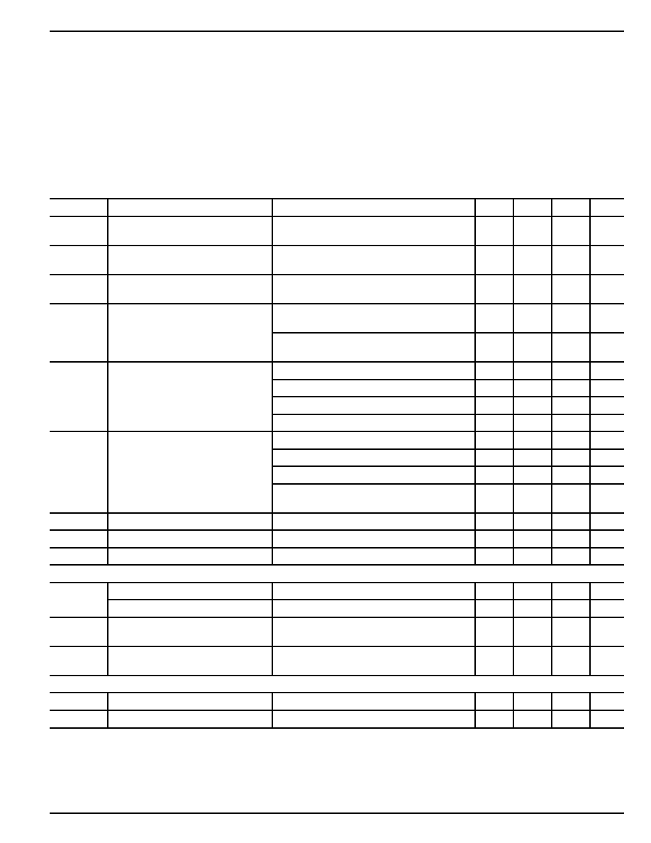
Electrical Characteristics
V
IN
= 6.0V; V
EN
= 2.0V; C
OUT
= 4.7
µ
F, I
OUT
= 100
µ
A; T
J
= 25
∞
C, bold values indicate ≠40
∞
C
T
J
+125
∞
C; unless noted.
Symbol
Parameter
Conditions
Min
Typ
Max
Units
V
OUT
Output Voltage Accuracy
variation from nominal V
OUT
≠1
1
%
≠2
+2
%
V
OUT
/
T
Output Voltage
Note 6
50
ppm/
∞
C
Temperature Coefficient
V
OUT
/V
OUT
Line Regulation
V
IN
= V
OUT
+ 1V to 30V
0.2
0.5
%
1.0
%
V
OUT
/V
OUT
Load Regulation
I
OUT
= 100
µ
A to 50mA, Note 7
0.15
0.3
%
0.5
%
I
OUT
= 100
µ
A to 150mA, Note 7
0.3
0.6
%
1.0
%
V
Dropout Voltage, Note 8
I
OUT
= 100
µ
A
50
100
mV
I
OUT
= 50mA
230
400
mV
I
OUT
= 100mA
270
mV
I
OUT
= 150mA
300
500
mV
I
GND
Ground Pin Current
V
EN
2.0V, I
OUT
= 100
µ
A
20
30
µ
A
V
EN
2.0V, I
OUT
= 50mA
0.5
0.8
mA
V
EN
2.0V, I
OUT
= 100mA
1.5
mA
V
EN
2.0V, I
OUT
= 150mA
2.8
4.0
mA
5.0
mA
I
GND(SHDN)
Ground Pin in Shutdown
V
EN
0.6V, V
IN
= 30V
0.1
1
µ
A
I
SC
Short Circuit Current
V
OUT
= 0V
260
350
mA
e
n
Output Noise
10Hz to 100kHz, V
OUT
= 3.0V, C
L
= 1.0
µ
F
160
µ
Vrms
/ERR Output
V
/ERR
Low Threshold
% of V
OUT
90
94
%
High Threshold
% of V
OUT
95
98
%
V
OL
/ERR Output Low Voltage
V
IN
= V
OUT(nom)
≠ 0.12V
OUT
, I
OL
= 200
µ
A
150
250
mV
400
mV
I
LEAK
/ERR Output Leakage
V
OH
= 30V
0.1
1
µ
A
2
µ
A
Enable Input
V
IL
Input Low Voltage
regulator off
0.6
V
V
IH
Input High Voltage
regulator on
2.0
V

MIC5236
Micrel
MIC5236
4
November 2000
Symbol
Parameter
Conditions
Min
Typ
Max
Units
I
IN
Enable Input Current
V
EN
= 0.6V, regulator off
0.01
1.0
µ
A
2.0
µ
A
V
EN
= 2.0V, regulator on
0.15
1.0
µ
A
2.0
µ
A
V
EN
= 30V, regulator on
0.5
2.5
µ
A
5.0
µ
A
Note 1.
Exceeding the absolute maximum rating may damage the device.
Note 2.
The device is not guaranteed to function outside its operating rating.
Note 3:
The absolute maximum positive supply voltage (60V) must be of limited duration (
100ms) and duty cycle (
1%). The maximum continuous
supply voltage is 30V.
Note 4:
The maximum allowable power dissipation of any T
A
(ambient temperature) is P
D(max)
= (T
J(max)
≠ T
A
)
˜
JA
. Exceeding the maximum
allowable power dissipation will result in excessive die termperature, and the regulator will go into thermal shutdown. The
JA
of the
MIC5236-x.xBM (all versions) is 63
∞
C/W, and the MIC5236-x.xBMM (all versions) is 80
∞
C/W, mounted on a PC board (see "Thermal Charac-
teristics" for further details).
Note 5.
Devices are ESD sensitive. Handling precautions recommended. Human body model, 1.5k in series with 100pF.
Note 6:
Output voltage temperature coefficient is defined as the worst-case voltage change divided by the total temperature range.
Note 7:
Regulation is measured at constant junction temperature using pulse testing with a low duty-cycle. Changes in output voltage due to heating
effects are covered by the specification for thermal regulation.
Note 8:
Dropout voltage is defined as the input to output differential at which the output voltage drops 2% below its nominal value measured at 1.0V
differential.
November 2000
5
MIC5236
MIC5236
Micrel
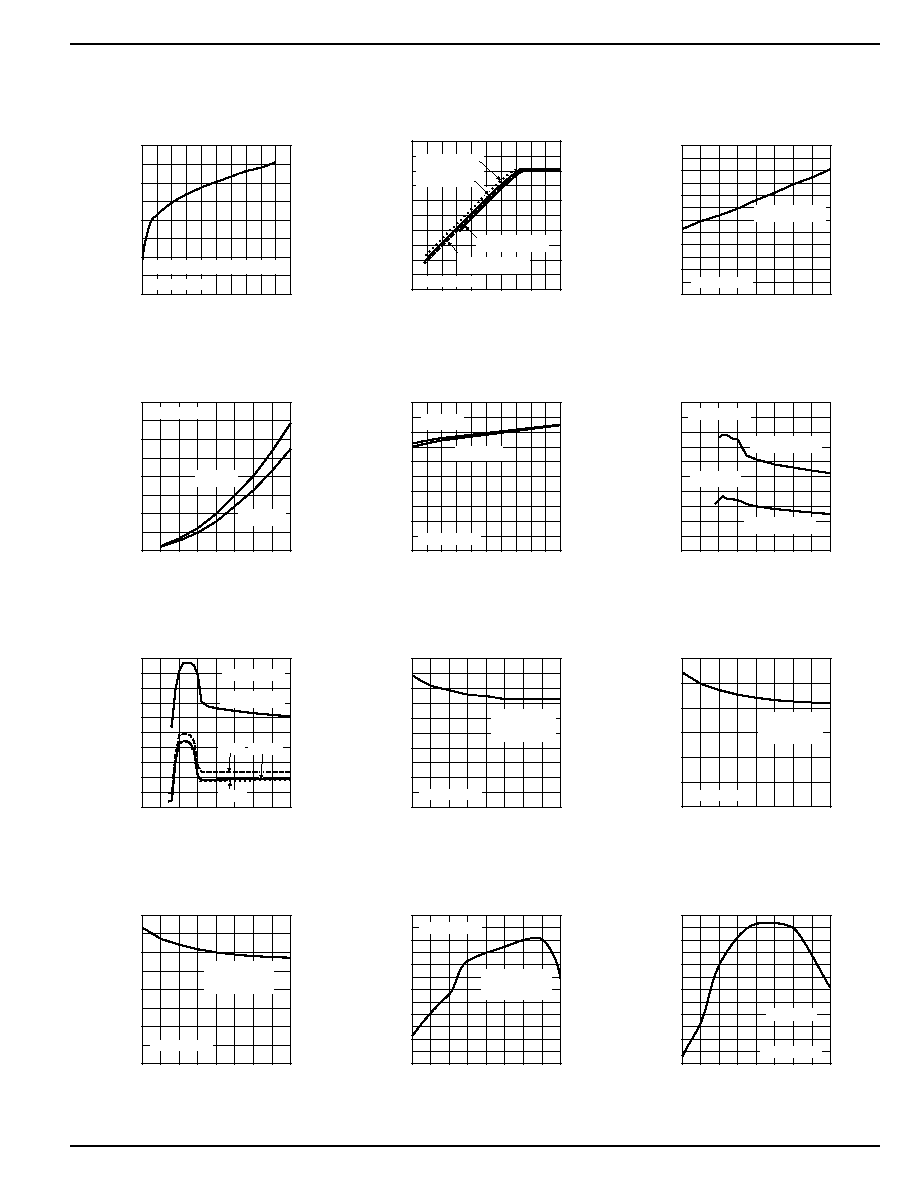
Typical Characteristics
0
100
200
300
400
0
40
80
120
160
200
DROPOUT VOLTAGE (mV)
OUTPUT CURRENT (mA)
Dropout Voltage
vs. Output Current
MIC5236-3.0
V
OUT
= 98% of Nominal V
OUT
1.0
1.5
2.0
2.5
3.0
3.5
1.5
2.0
2.5
3.0
3.5
4.0
OUTPUT VOLTAGE (V)
SUPPLY VOLTAGE (V)
Dropout Characteristics
I
LOAD
= 10mA
I
LOAD
= 50mA
I
LOAD
= 100mA
I
LOAD
= 150mA
MIC5236-3.0
0
100
200
300
400
500
600
-40 -20 0
20 40 60 80 100 120
DROPOUT VOLTAGE (mV)
TEMPERATURE (
∞
C)
Dropout Voltage
vs. Temperature
I
LOAD
= 150mA
MIC5236-3.0
0
1
2
3
4
0
20 40 60 80 100 120 140 160
GROUND PIN CURRENT (mA)
OUTPUT CURRENT (mA)
Ground Current
vs. Output Current
V
IN
= 4V
V
IN
= 10V
MIC5236-3.0
0
5
10
15
20
25
0
100
200
300
400
500
GROUND PIN CURRENT (
µ
A)
OUTPUT CURRENT (
µ
A)
Ground Pin Current
vs. Output Current
V
IN
= 10V
V
IN
= 4V
MIC5236-3.0
0
1
2
3
4
5
0
1
2
3
4
5
6
7
8
GROUND CURRENT (mA)
SUPPLY VOLTAGE (V)
Ground Current
vs. Supply Voltage
I
LOAD
= 100
µ
A
V
OUT
= 3V
MIC5236-3.0
I
LOAD
= 150mA
0
10
20
30
40
50
60
70
80
90
100
0
1
2
3
4
5
6
7
8
GROUND PIN CURRENT (
µ
A)
SUPPLY VOLTAGE (V)
Ground Current
vs. Supply Voltage
I
LOAD
= 10mA
MIC5236-3.0
1mA
100
µ
A
10
µ
A
0
0.02
0.04
0.06
0.08
0.10
-40 -20 0
20 40 60 80 100 120
GROUND CURRENT (mA)
TEMPERATURE (
∞
C)
Ground Current
vs. Temperature
V
IN
= 4V
I
LOAD
= 10mA
MIC5236-3.0
0
0.2
0.4
0.6
0.8
1.0
1.2
-40 -20 0
20 40 60 80 100 120
GROUND CURRENT (mA)
TEMPERATURE (
∞
C)
Ground Current
vs. Temperature
V
IN
= 4V
I
LOAD
= 75mA
MIC5236-3.0
0
1
2
3
4
-40 -20 0
20 40 60 80 100 120
GROUND CURRENT (mA)
TEMPERATURE (
∞
C)
Ground Current
vs. Temperature
V
IN
= 4V
I
LOAD
= 150mA
MIC5236-3.0
2.985
2.990
2.995
3.000
3.005
3.010
3.015
-40 -20 0
20 40 60 80 100 120
VOLTAGE OUTPUT (V)
TEMPERATURE (
∞
C)
Output Voltage
vs. Temperature
V
IN
= 4V
I
LOAD
= 150mA
MIC5236-3.0
255
260
265
270
275
280
285
-40 -20 0
20 40 60 80 100 120
SHORT CIRCUIT CURRENT (mA)
TEMPERATURE (
∞
C)
Short Circuit Current
vs. Temperature
V
OUT
= 0V
MIC5236-3.0

MIC5236
Micrel
MIC5236
6
November 2000
3.002
3.004
3.006
3.008
3.010
3.012
3.014
3.016
3.018
0
5
10
15
20
25
30
35
VOLTAGE OUTPUT (V)
INPUT VOLTAGE (V)
Line Regulation
I
LOAD
= 10mA
MIC5236-3.0
36
37
38
39
40
41
-40 -20 0
20 40 60 80 100 120
INPUT VOLTAGE (V)
TEMPERATURE (
∞
C)
Overvoltage Threshold
vs. Temperature
MIC5236-3.0
0
0.5
1.0
1.5
2.0
2.5
3.0
3.5
0
100
200
300
400
OUTPUT VOLTAGE (V)
CURRENT LIMIT (mA)
Current Limit
vs. Output Voltage
MIC5236-3.0
0
20
40
60
80
100
120
-30
-20
-10
0
10
INPUT CURRENT (mA)
INPUT VOLTAGE (V)
Input Current
V
EN
= 5V
R
L
= 30
MIC5236-3.0
0
0.5
1.0
1.5
2.0
2.5
3.0
0
0.5
1.0
1.5
2.0
OUTPUT-LOW VOLTAGE (V)
SINK CURRENT (mA)
Dropout Induced
Error Flag
V
IN
= 2.7V
V
OUT
=2.62V
No Load
MIC5236-3.0
0
0.25
0.50
0.75
1.00
1.25
0
0.5
1.0
1.5
2.0
2.5
3.0
OUTPUT-LOW VOLTAGE (V)
SINK CURRENT (mA)
Current Limit Induced
Error Flag
V
IN
= 6V
V
OUT
= 2.03V
R
L
= 6
MIC5236-3.0
0
10
20
30
40
50
60
70
0
5
10
15
20
REVERSE CURRENT (
µ
A)
EXTERNAL VOLTAGE (V)
Reverse Current
(Grounded Input)
-40
∞
C
+25
∞
C
+85
∞
C
Note 11
0
10
20
30
40
50
60
0
5
10
15
20
REVERSE CURRENT (
µ
A)
EXTERNAL VOLTAGE (V)
Reverse Current
(Open Input)
-40
∞
C
+25
∞
C
+85
∞
C
Note 10
Note 10
Note 11
IN
MIC5236
OUT
GND
Reverse
Current
EN
IN
MIC5236
OUT
GND
Reverse
Current
EN
November 2000
7
MIC5236
MIC5236
Micrel
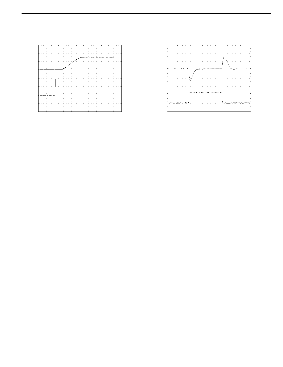
Functional Characteristics
Enable
Transient Response
TIME (250
µ
s/div.)
V
EN
(5V/div
.
)
V
OUT
(2V/div
.
)
V
IN
= 5V
I
L
= 10mA
Load
Transient Response
TIME (250
µ
s/div.)
I
OUT
(100mA/div
.
)
V
OUT
(100mV/div
.
)
V
IN
= 4V
V
OUT
= 3V
C
OUT
= 15
µ
F
ESR = 200m
MIC5236
Micrel
MIC5236
8
November 2000
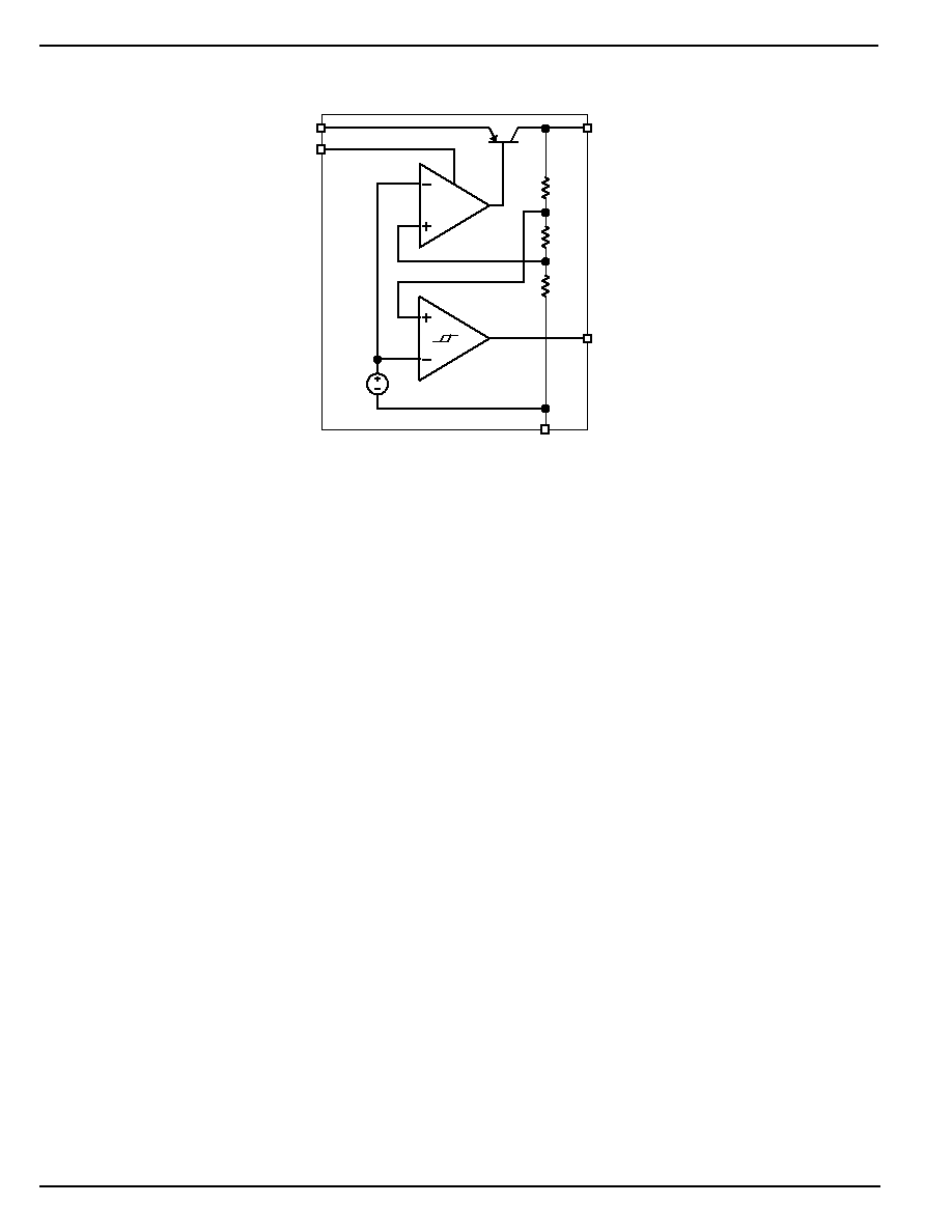
Functional Diagram
R
FB1
Error
Amplifier
Error
Comparator
V
REF
1.23V
R
FB2
R
FB3
OUT
ERR
GND
MIC5236-x.x
IN
EN

November 2000
9
MIC5236
MIC5236
Micrel
Application Information
The MIC5236 provides all of the advantages of the MIC2950:
wide input voltage range, load dump (positive transients up to
60V), and reversed-battery protection, with the added advan-
tages of reduced quiescent current and smaller package.
Additionally, when disabled, quiescent current is reduced to
0.1
µ
A.
Enable
A low on the enable pin disables the part, forcing the quies-
cent current to less than 0.1
µ
A. Thermal shutdown and the
error flag are not functional while the device is disabled. The
maximum enable bias current is 2
µ
A for a 2.0V input. An open
collector pull-up resistor tied to the input voltage should be set
low enough to maintain 2V on the enable input. Figure 1
shows an open collector output driving the enable pin through
a 200k pull-up resistor tied to the input voltage.
In order to avoid output oscillations, slow transitions from low
to high should be avoided.
C
OUT
V
OUT
V
IN
5V
V
ERR
IN
MIC5236
EN
200k
200k
OUT
GND
SHUTDOWN
ENABLE
ERR
Figure 1. Remote Enable
Input Capacitor
An input capacitor may be required when the device is not
near the source power supply or when supplied by a battery.
Small, surface mount, ceramic capacitors can be used for
bypassing. Larger values may be required if the source
supply has high ripple.
Output Capacitor
The MIC5236 has been designed to minimize the effect of the
output capacitor ESR on the closed loop stability. As a result,
ceramic or film capacitors can be used at the output. Figure 2
displays a range of ESR values for a 10
µ
F capacitor. Virtually
any 10
µ
F capacitor with an ESR less than 3.4
is sufficient
for stability over the entire input voltage range. Stability can
also be maintained throughout the specified load and line
conditions with 1
µ
F film or ceramic capacitors.
0
1
2
3
4
5
5
10
15
20
25
30
OUTPUT CAPACITOR ESR (
)
INPUT VOLTAGE (V)
Stable Region
T
J
= 25
∞
C
V
OUT
= 10
µ
F
Figure 2. Output Capacitor ESR
Error Detection Comparator Output
The ERR pin is an open collector output which goes low when
the output voltage drops 5% below it's internally programmed
level. It senses conditions such as excessive load (current
limit), low input voltage, and over temperature conditions.
Once the part is disabled via the enable input, the error flag
output is not valid. Overvoltage conditions are not reflected in
the error flag output. The error flag output is also not valid for
input voltages less than 2.3V.
The error output has a low voltage of 400mV at a current of
200
µ
A. In order to minimize the drain on the source used for
the pull-up, a value of 200k to 1M
is suggested for the error
flag pull-up. This will guarantee a maximum low voltage of
0.4V for a 30V pull-up potential. An unused error flag can be
left unconnected.
NOT
VALID
NOT
VALID
VALID ERROR
Error
Output
Input
Voltage
Output
Voltage
4.75V
0V
0V
5V
1.3V
Figure 3. Error Output Timing
Reverse Current Protection
The MIC5236 is designed to limit the reverse current flow
from output to input in the event that the MIC5236 output has
been tied to the output of another power supply. See the
graphs detailing the reverse current flow with the input
grounded and open.
Thermal Shutdown
The MIC5236 has integrated thermal protection. This feature
is only for protection purposes. The device should never be
intentionally operated near this temperature as this may have
detrimental effects on the life of the device. The thermal
shutdown may become inactive while the enable input is
transitioning a high to a low. When disabling the device via the
enable pin, transition from a high to low quickly. This will
insure that the output remains disabled in the event of a
thermal shutdown.
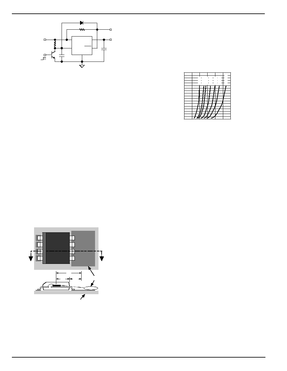
Current Limit
Figure 4 displays a method for reducing the steady state
short circuit current. The duration that the supply delivers
current is set by the time required for the error flag output to
discharge the 4.7
µ
F capacitor tied to the enable pin. The off
time is set by the 200K resistor as it recharges the 4.7
µ
F
capacitor, enabling the regulator. This circuit reduces the
short circuit current from 280mA to 15mA while allowing for
regulator restart once the short is removed.
MIC5236
Micrel
MIC5236
10
November 2000
C
OUT
V
OUT
V
IN
5V
V
ERR
IN
MIC5236
EN
200k
1N4148
200k
4.7
µ
F
OUT
GND
SHUTDOWN
ENABLE
ERR
Figure 4. Remote Enable with Short-Circuit
Current Foldback
Thermal Characteristics
The MIC5236 is a high input voltage device, intended to
provide 150mA of continuous output current in two very small
profile packages. The power SOP-8 and power MSOP-8
allow the device to dissipate about 50% more power than
their standard equivalents.
Power SOP-8 Thermal Characteristics
One of the secrets of the MIC5236's performance is its power
SO-8 package featuring half the thermal resistance of a
standard SO-8 package. Lower thermal resistance means
more output current or higher input voltage for a given
package size.
Lower thermal resistance is achieved by joining the four
ground leads with the die attach paddle to create a single-
piece electrical and thermal conductor. This concept has
been used by MOSFET manufacturers for years, proving
very reliable and cost effective for the user.
Thermal resistance consists of two main elements,
JC
(junction-to-case thermal resistance) and
CA
(case-to-ambi-
ent thermal resistance). See Figure 5.
JC
is the resistance
from the die to the leads of the package.
CA
is the resistance
from the leads to the ambient air and it includes
CS
(case-to-
sink thermal resistance) and
SA
(sink-to-ambient thermal
resistance).
JA
JC
CA
printed circuit board
ground plane
heat sink area
SOP-8
AMBIENT
Figure 5. Thermal Resistance
Using the power SOP-8 reduces the
JC
dramatically and
allows the user to reduce
CA
. The total thermal resistance,
JA
(junction-to-ambient thermal resistance) is the limiting-
factor in calculating the maximum power dissipation capabil-
ity of the device. Typically, the power SOP-8 has a
JC
of
20
∞
C/W, this is significantly lower than the standard SOP-8
which is typically 75
∞
C/W.
CA
is reduced because pins 5
through 8 can now be soldered directly to a ground plane
which significantly reduces the case-to-sink thermal resis-
tance and sink to ambient thermal resistance.
Low-dropout linear regulators from Micrel are rated to a
maximum junction temperature of 125
∞
C. It is important not
to exceed this maximum junction temperature during opera-
tion of the device. To prevent this maximum junction tempera-
ture from being exceeded, the appropriate ground plane heat
sink must be used.
0
100
200
300
400
500
600
700
800
900
0
0.25 0.50 0.75 1.00 1.25 1.50
COPPER AREA (mm
2
)
POWER DISSIPATION (W)
40
∞
C
50
∞
C
55
∞
C
65
∞
C
75
∞
C
85
∞
C
100
∞
C
Figure 6. Copper Area vs. Power-SOP
Power Dissipation
(
T
JA
)
Figure 6 shows copper area versus power dissipation with
each trace corresponding to a different temperature rise
above ambient.
From these curves, the minimum area of copper necessary
for the part to operate safely can be determined. The maxi-
mum allowable temperature rise must be calculated to deter-
mine operation along which curve.
T = T
J(max)
≠ T
A(max)
T
J(max)
= 125
∞
C
T
A(max)
= maximum ambient operating temperature
For example, the maximum ambient temperature is 50
∞
C, the
T is determined as follows:
T = 125
∞
C ≠ 50
∞
C
T = 75
∞
C
Using Figure 6, the minimum amount of required copper can
be determined based on the required power dissipation.
Power dissipation in a linear regulator is calculated as fol-
lows:
P
D
= (V
IN
≠ V
OUT
) I
OUT
+ V
IN
∑ I
GND
If we use a 3V output device and a 28V input at moderate
output current of 25mA, then our power dissipation is as
follows:
P
D
= (28V ≠ 3V)
◊
25mA + 28V
◊
250
µ
A
P
D
= 625mW + 7mW
P
D
= 632mW
From Figure 6, the minimum amount of copper required to
operate this application at a
T of 75
∞
C is 25mm
2
.
Quick Method
Determine the power dissipation requirements for the design
along with the maximum ambient temperature at which the
device will be operated. Refer to Figure 7, which shows safe
operating curves for three different ambient temperatures:
25
∞
C, 50
∞
C and 85
∞
C. From these curves, the minimum
November 2000
11
MIC5236
MIC5236
Micrel
amount of copper can be determined by knowing the maxi-
mum power dissipation required. If the maximum ambient
temperature is 50
∞
C and the power dissipation is as above,
632mW, the curve in Figure 7 shows that the required area of
copper is 25mm
2
.
The
JA
of this package is ideally 63
∞
C/W, but it will vary
depending upon the availability of copper ground plane to
which it is attached.
0
100
200
300
400
500
600
700
800
900
0
0.25 0.50 0.75 1.00 1.25 1.50
COPPER AREA (mm
2
)
POWER DISSIPATION (W)
85
∞
C
50
∞
C
25
∞
C
T
J
= 125
∞
C
Figure 7. Copper Area vs. Power-SOP
Power Dissipation (T
A
)
0
100
200
300
400
500
600
700
800
900
0
0.25 0.50 0.75 1.00 1.25 1.50
COPPER AREA (mm
2
)
POWER DISSIPATION (W)
40
∞
C
50
∞
C
55
∞
C
65
∞
C
75
∞
C
85
∞
C
100
∞
C
Figure 8. Copper Area vs. Power-MSOP
Power Dissipation
(
T
JA
)
The same method of determining the heat sink area used for
the power-SOP-8 can be applied directly to the power-
MSOP-8. The same two curves showing power dissipation
versus copper area are reproduced for the power-MSOP-8
and they can be applied identically, see Figures 8 and 9.
0
100
200
300
400
500
600
700
800
900
0
0.25 0.50 0.75 1.00 1.25 1.50
COPPER AREA (mm
2
)
POWER DISSIPATION (W)
85
∞
C
50
∞
C 25
∞
C
T
J
= 125
∞
C
Figure 9. Copper Area vs. Power-MSOP
Power Dissipation (T
A
)
Power MSOP-8 Thermal Characteristics
The power-MSOP-8 package follows the same idea as the
power-SO-8 package, using four ground leads with the die
attach paddle to create a single-piece electrical and thermal
conductor, reducing thermal resistance and increasing power
dissipation capability.
Quick Method
Determine the power dissipation requirements for the design
along with the maximum ambient temperature at which the
device will be operated. Refer to Figure 9, which shows safe
operating curves for three different ambient temperatures,
25
∞
C, 50
∞
C, and 85
∞
C. From these curves, the minimum
amount of copper can be determined by knowing the maxi-
mum power dissipation required. If the maximum ambient
temperature is 50
∞
C, and the power dissipation is 639mW,
the curve in Figure 9 shows that the required area of copper
is 110mm
2
,when using the power MSOP-8.
Adjustable Regulator Application
MIC5236BM/MM
EN
GND
OUT
IN
V
IN
2
4
1
3
5-8
V
R1
R2
1
µ
F
OUT
ADJ
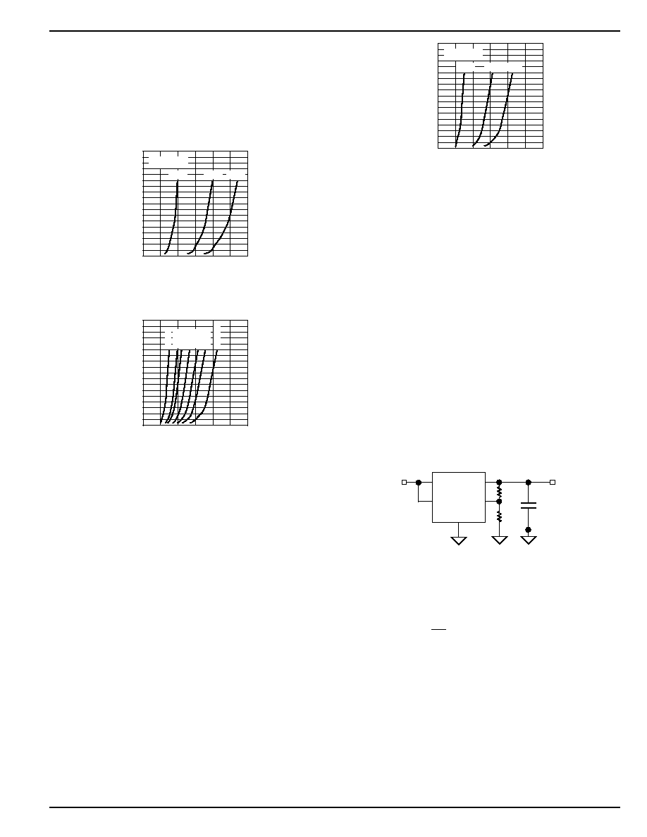
Figure 10. Adjustable Voltage Application
The MIC5236BM/MM can be adjusted from 1.24V to 20V by
using two external resistors (Figure 10). The resistors set the
output voltage based on the following equation:
V
OUT
= V
REF
(1 +
R
R
1
2
)
Where V
REF
= 1.23V.
MIC5236
Micrel
MIC5236
12
November 2000
MICREL INC.
1849 FORTUNE DRIVE
SAN JOSE, CA 95131
USA
TEL
+ 1 (408) 944-0800
FAX
+ 1 (408) 944-0970
WEB
http://www.micrel.com
This information is believed to be accurate and reliable, however no responsibility is assumed by Micrel for its use nor for any infringement of patents or
other rights of third parties resulting from its use. No license is granted by implication or otherwise under any patent or patent right of Micrel Inc.
© 2000 Micrel Incorporated
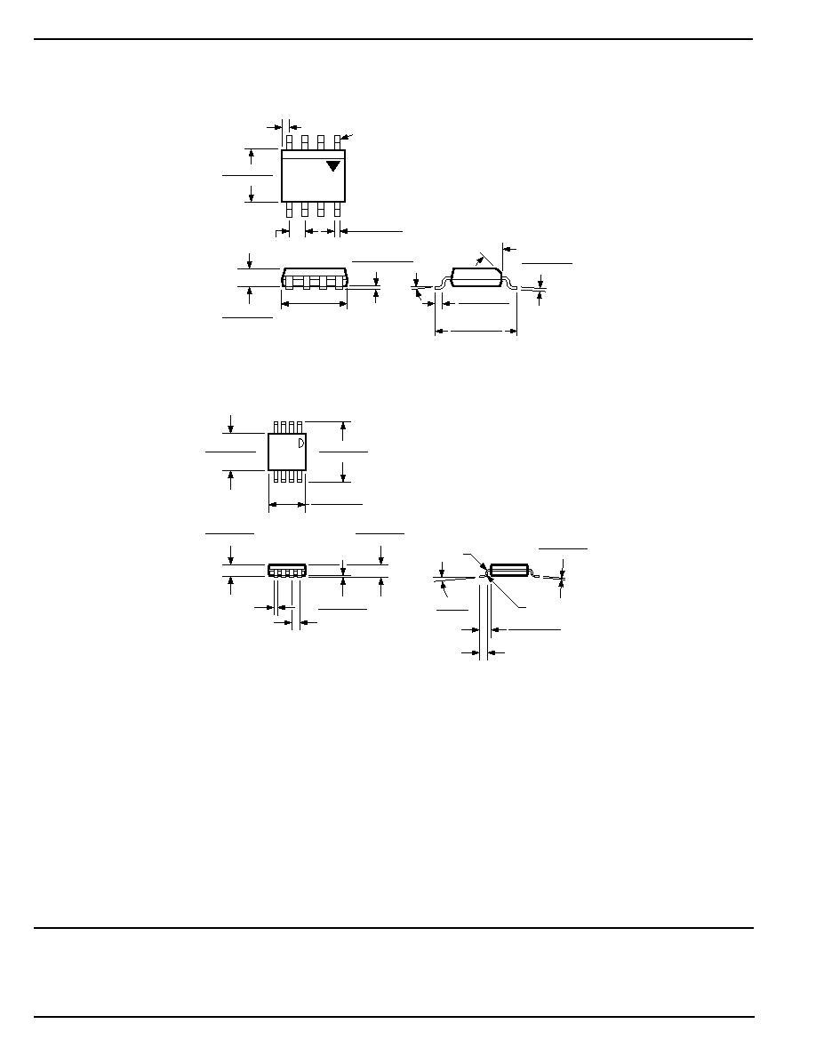
Package Information
45
∞
0
∞
≠8
∞
0.244 (6.20)
0.228 (5.79)
0.197 (5.0)
0.189 (4.8)
SEATING
PLANE
0.026 (0.65)
MAX
)
0.010 (0.25)
0.007 (0.18)
0.064 (1.63)
0.045 (1.14)
0.0098 (0.249)
0.0040 (0.102)
0.020 (0.51)
0.013 (0.33)
0.157 (3.99)
0.150 (3.81)
0.050 (1.27)
TYP
PIN 1
DIMENSIONS:
INCHES (MM)
0.050 (1.27)
0.016 (0.40)
8-Lead SOIC (M)
0.008 (0.20)
0.004 (0.10)
0.039 (0.99)
0.035 (0.89)
0.021 (0.53)
0.012 (0.03) R
0.0256 (0.65) TYP
0.012 (0.30) R
5
∞
MAX
0
∞
MIN
0.122 (3.10)
0.112 (2.84)
0.120 (3.05)
0.116 (2.95)
0.012 (0.03)
0.007 (0.18)
0.005 (0.13)
0.043 (1.09)
0.038 (0.97)
0.036 (0.90)
0.032 (0.81)
DIMENSIONS:
INCH (MM)
0.199 (5.05)
0.187 (4.74)
8-Lead MSOP (MM)