January 2000
1
MIC5237
MIC5237
Micrel
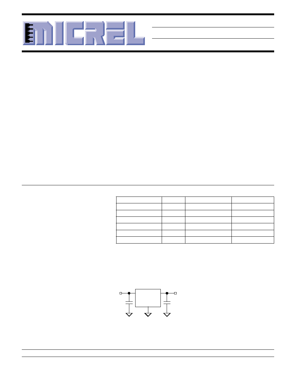
Typical Application
MIC5237
500mA Low-Dropout Regulator
Preliminary Information
General Description
The MIC5237 is a general-purpose low-dropout regulator
capable of 500mA output current with better than 3% output
voltage accuracy. Using Micrel's proprietary Super
þeta PNPTM process with a PNP pass element, these regu-
lators feature less than 300mV dropout voltage and typically
8mA ground current at full load.
Designed for applications that require moderate current over
a broad input voltage range, including hand-held and battery-
powered devices, the MIC5237 is intended for applications
that can tolerate moderate voltage drop at higher current.
Key features include low ground current to help prolong
battery life, reversed-battery protection, current limiting, over-
temperature shutdown, and thermally efficient packaging.
The MIC5237 is available in fixed output voltages only.
For space-critical applications and improved performance,
see the MIC5209 and MIC5219. For output current require-
ments up to 750mA, see the MIC2937.
Features
∑ Guaranteed 500mA output over the full operating
temperature range
∑ Low 300mV typical dropout voltage at full load
∑ Extremely tight load and line regulation
∑ Current and thermal limiting
∑ Reversed-battery protection
∑ TO-220 and TO-263 packages
∑ Low temperature coefficient
∑ No-load stability
∑ Low-noise output
Applications
∑ Portable and laptop computers
∑ Desktop computer
∑ Battery chargers
∑ SMPS post-regulator/dc-to-dc modules
∑ Consumer and personal electronics
Ordering Information
Part Number
Voltage
Junct. Temp. Range
Package
MIC5237-2.5BT
2.5V
≠40
∞
C to +125
∞
C
TO-220
MIC5237-2.5BU
2.5V
≠40
∞
C to +125
∞
C
TO-263
MIC5237-3.3BT
3.3V
≠40
∞
C to +125
∞
C
TO-220
MIC5237-3.3BU
3.3V
≠40
∞
C to +125
∞
C
TO-263
MIC5237-5.0BT
5.0V
≠40
∞
C to +125
∞
C
TO-220
MIC5237-5.0BU
5.0V
≠40
∞
C to +125
∞
C
TO-263
MIC5237-5.0
IN
OUT
GND
1.0µF
1.0µF
tantalum
V
IN
5.6V
V
OUT
5.0V
±
3%
Micrel, Inc. ∑ 1849 Fortune Drive ∑ San Jose, CA 95131 ∑ USA ∑ tel + 1 (408) 944-0800 ∑ fax + 1 (408) 944-0970 ∑ http://www.micrel.com
MIC5237
Micrel
MIC5237
2
January 2000
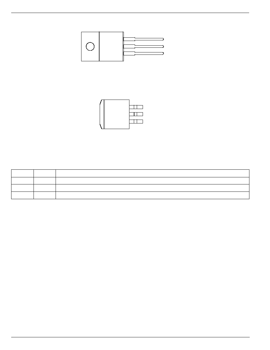
Pin Description
Pin No.
Pin Name
Pin Function
1
IN
Supply Input
2,
TAB
GND
Ground: TO-220 and TO-263 pin 2 and
TAB
are internally connected.
3
OUT
Regulator Output
Pin Configuration
TAB
3
OUT
2
GND
1
IN
MIC5237-x.xBT
(TO-220-3)
TAB
3
OUT
2
GND
1
IN
MIC5237-x.xBU
(TO-263-3)
Absolute Maximum Ratings
Input Voltage (V
IN
) ........................................ ≠20V to +20V
Power Dissipation (P
D
) ............................ Internally Limited
Junction Temperature (T
J
) ....................... ≠40
∞
C to +125
∞
C
Lead Temperature (soldering, 5 sec.) ....................... 260
∞
C
Operating Ratings
Input Voltage (V
IN
) ....................................... +2.5V to +16V
Junction Temperature (T
J
) ....................... ≠40
∞
C to +125
∞
C
Package Thermal Resistance
TO-220 (
JA
) ....................................................... 55
∞
C/W
TO-220 (
JC
) ......................................................... 3
∞
C/W
TO-263 (
JC
) ......................................................... 3
∞
C/W
January 2000
3
MIC5237
MIC5237
Micrel
Electrical Characteristics
V
IN
= V
OUT
+ 1.0V; C
OUT
= 4.7
µ
F, I
OUT
= 100
µ
A; T
J
= 25
∞
C, bold values indicate ≠40
∞
C
T
J
+125
∞
C; unless noted.
Symbol
Parameter
Conditions
Min
Typical
Max
Units
V
OUT
Output Voltage Accuracy
variation from nominal V
OUT
≠3
3
%
≠5
5
%
V
OUT
/
T
Output Voltage
Note 2
40
ppm/
∞
C
Temperature Coefficient
V
OUT
/V
OUT
Line Regulation
V
IN
= V
OUT
+ 1V to 16V
0.05
%/V
0.015
0.1
%/V
V
OUT
/V
OUT
Load Regulation
I
OUT
= 100
µ
A to 500mA, Note 3
0.05
0.5
%
0.7
%
V
IN
≠ V
OUT
Dropout Voltage, Note 4
I
OUT
= 100
µ
A
10
70
mV
90
mV
I
OUT
= 50mA
115
190
mV
280
mV
I
OUT
= 150mA
165
350
mV
450
mV
I
OUT
= 500mA
300
600
mV
700
mV
I
GND
Ground Pin Current, Note 5
I
OUT
= 100
µ
A
80
130
µ
A
170
µ
A
I
OUT
= 50mA
350
650
µ
A
900
µ
A
I
OUT
= 150mA
1.8
2.5
mA
3.0
mA
I
OUT
= 500mA
8
15
mA
20
mA
PSRR
Ripple Rejection
f = 120Hz
75
dB
I
LIMIT
Current Limit
V
OUT
= 0V
700
900
mA
1000
V
OUT
/
P
D
Thermal Regulation
Note 6
0.05
%/W
e
no
Output Noise
V
OUT
= 5.0V, I
OUT
= 50mA,
500
nV/ Hz
C
OUT
= 2.2
µ
F
Note 1:
Absolute maximum ratings indicate limits beyond which damage to the component may occur. Electrical specifications do not apply when
operating the device outside of its operating ratings. The maximum allowable power dissipation is a function of the maximum junction
temperature, T
J(max)
, the junction-to-ambient thermal resistance,
JA
, and the ambient temperature, T
A
. The maximum allowable power
dissipation at any ambient temperature is calculated using: P
D(max)
= (T
J(max)
≠ T
A
)
˜
JA
. Exceeding the maximum allowable power dissipa-
tion will result in excessive die temperature, and the regulator will go into thermal shutdown. See the "Thermal Considerations" section for
details.
Note 2:
Output voltage temperature coefficient is defined as the worst case voltage change divided by the total temperature range.
Note 3:
Regulation is measured at constant junction temperature using low duty cycle pulse testing. Parts are tested for load regulation in the load
range from 100
µ
A to 500mA. Changes in output voltage due to heating effects are covered by the thermal regulation specification.
Note 4:
Dropout voltage is defined as the input to output differential at which the output voltage drops 2% below its nominal value measured at 1V
differential.
Note 5:
Ground pin current is the regulator quiescent current plus pass transistor base current. The total current drawn from the supply is the sum of
the load current plus the ground pin current.
Note 6:
Thermal regulation is defined as the change in output voltage at a time "t" after a change in power dissipation is applied, excluding load or line
regulation effects. Specifications are for a 500mA load pulse at V
IN
= 16V for t = 10ms.
MIC5237
Micrel
MIC5237
4
January 2000
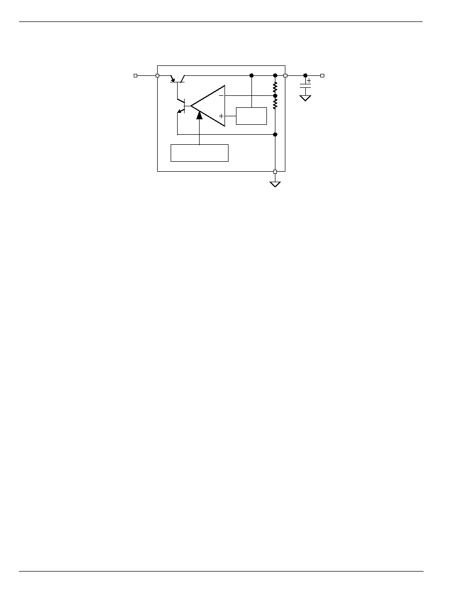
Block Diagram
Current Limit
Thermal Shutdown
IN
OUT
GND
Bandgap
Ref.
C
OUT
V
OUT
V
IN
MIC5237-x.x
Fixed Regulator
January 2000
5
MIC5237
MIC5237
Micrel
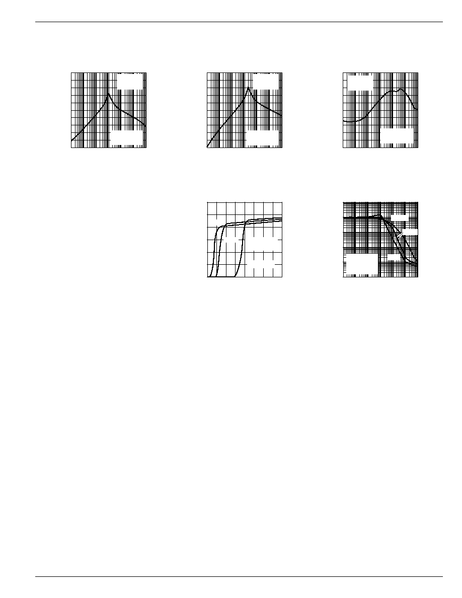
Typical Characteristics
-100
-80
-60
-40
-20
0
1E+1 1E+2 1E+3 1E+4 1E+5 1E+6 1E+7
PSRR (dB)
FREQUENCY (Hz)
Power Supply
Rejection Ratio
I
OUT
= 100
µ
A
C
OUT
= 1
µ
F
V
IN
= 6V
V
OUT
= 5V
10
100
1k
10k 100k 1M 10M
-100
-80
-60
-40
-20
0
1E+1 1E+2 1E+3 1E+4 1E+5 1E+6 1E+7
PSRR (dB)
FREQUENCY (Hz)
Power Supply
Rejection Ratio
I
OUT
= 1mA
C
OUT
= 1
µ
F
V
IN
= 6V
V
OUT
= 5V
10
100
1k
10k 100k 1M 10M
-100
-80
-60
-40
-20
0
1E+1 1E+2 1E+3 1E+4 1E+5 1E+6 1E+7
PSRR (dB)
FREQUENCY (Hz)
Power Supply
Rejection Ratio
I
OUT
= 100mA
C
OUT
= 1
µ
F
V
IN
= 6V
V
OUT
= 5V
10
100
1k
10k 100k 1M 10M
0
10
20
30
40
50
60
0
0.1
0.2
0.3
0.4
RIPPLE REJECTION (dB)
VOLTAGE DROP (V)
Power Supply Ripple Rejection
vs. Voltage Drop
I
OUT
= 100mA
10mA
1mA
C
OUT
= 1
µ
F
0.0001
0.001
0.01
0.1
1
10
1E+1 1E+2 1E+3 1E+4 1E+5 1E+6 1E+7
NOISE (
µ
V/
Hz)
FREQUENCY (Hz)
Noise Performance
10mA
1mA
100mA
10
100
1k
10k 100k 1M 10M
V
OUT
= 5V
C
OUT
= 10
µ
F
electrolytic