August 2003
1
MIC5238
MIC5238
Micrel
MIC5238
Ultra-Low Quiescent Current, 150mA
µ
Cap LDO Regulator
General Description
The MIC5238 is an ultra-low voltage output, 150mA LDO
regulator. Designed to operate in a single supply or dual
supply mode, the MIC5238 consumes only 23
µ
A of bias
current, improving efficiency. When operating in the dual
supply mode, the efficiency greatly improves as the higher
voltage supply is only required to supply the 23
µ
A bias
current while the output and base drive comes off of the much
lower input supply voltage.
As a
µ
Cap regulator, the MIC5238 operates with a 2.2
µ
F
ceramic capacitor on the output, offering a smaller overall
solution. It also incorporates a logic-level enable pin that
allows the MIC5238 to be put into a zero off-current mode
when disabled.
The MIC5238 is fully protected with current limit and thermal
shutdown. It is offered in the IttyBittyTM SOT-23-5 package
with an operating junction temperature range of
≠40
∞
C to +125
∞
C.
Micrel, Inc. ∑ 1849 Fortune Drive ∑ San Jose, CA 95131 ∑ USA ∑ tel + 1 (408) 944-0800 ∑ fax + 1 (408) 944-0970 ∑ http://www.micrel.com
IttyBitty is a trademark of Micrel, Inc.
Features
∑ Ultra-low input voltage range: 1.5V to 6V
∑ Ultra-low output voltage: 1.1V minimum output voltage
∑ Low dropout voltage: 310mV at 150mA
∑ High output accuracy:
±
2.0% over temperature
∑
µ
Cap: stable with ceramic or tantalum capacitors
∑ Excellent line and load regulation specifications
∑ Zero shutdown current
∑ Reverse leakage protection
∑ Thermal shutdown and current limit protection
∑ IttyBittyTM SOT-23-5 package
Applications
∑ PDAs and pocket PCs
∑ Cellular phones
∑ Battery powered systems
∑ Low power microprocessor power supplies
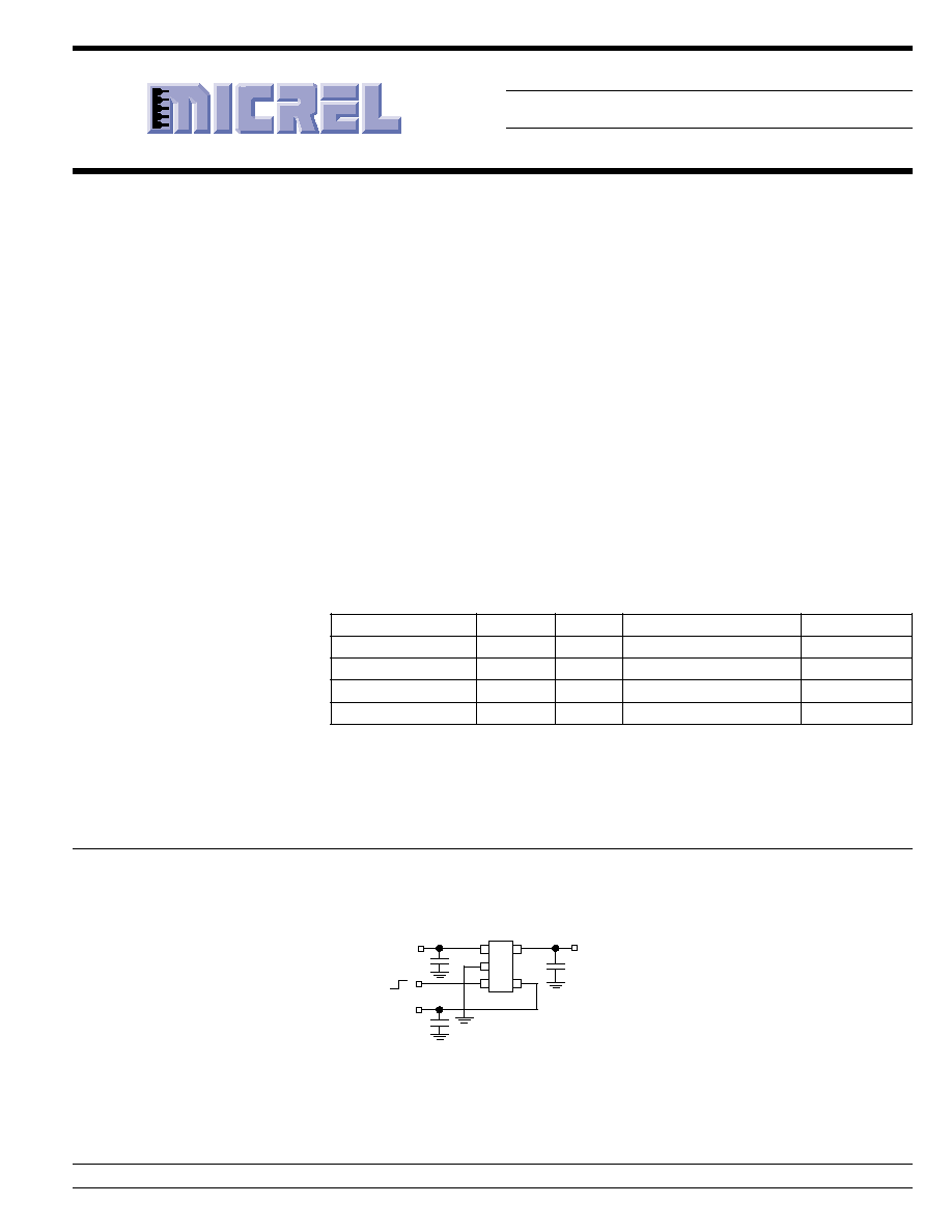
Typical Application
1
5
2
3
4
C
OUT
=2.2
µ
F
ceramic
C
IN
V
BIAS
=2.5V
EN
MIC5238-1.0BM5
V
IN
=1.5V
1.0V
C
BIAS
OFF ON
Ultra-Low Voltage Application
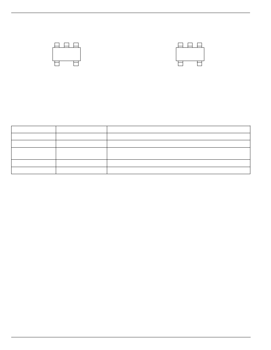
Ordering Information
Part Number
Marking
Voltage*
Junction Temp. Range
Package*
MIC5238-1.1BM5
L411
1.1V
≠40
∞
C to +125
∞
C
SOT-23-5
MIC5238-1.3BM5
L413
1.3V
≠40
∞
C to +125
∞
C
SOT-23-5
MIC5238-1.1BD5
N411
1.1V
≠40
∞
C to +125
∞
C
TSOT-23-5
MIC5238-1.3BD5
N413
1.3V
≠40
∞
C to +125
∞
C
TSOT-23-5
* For other voltages and package option contact the factory
August 2003
3
MIC5238
MIC5238
Micrel
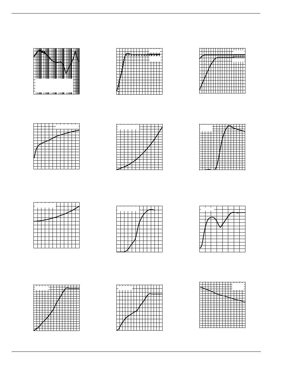
Electrical Characteristics
(Note 4)
T
A
= 25
∞
C with V
IN
= V
OUT
+ 1V; V
BIAS
= 3.3V; I
OUT
= 100
µ
A; V
EN
= 2V, Bold values indicate ≠40
∞
C < T
J
< +125
∞
C; unless otherwise specified.
Parameter
Condition
Min.
Typ.
Max.
Units
Output Voltage Accuracy
Variation from nominal V
OUT
≠1.5
+1.5
%
≠2
+2
%
Line Regulation
V
BIAS
= 2.3V to 6V, Note 5
0.25
0.5
%
Input Line Regulation
V
IN
= (V
OUT
+ 1V) to 6V
0.04
%
Load Regulation
Load = 100
µ
A to 150mA
0.7
1
%
Dropout Voltage
I
OUT
= 100
µ
A
50
mV
I
OUT
= 50mA
230
300
mV
400
mV
I
OUT
= 100mA
270
mV
mV
I
OUT
= 150mA
310
450
mV
500
mV
BIAS Current, Note 6
I
OUT
= 100
µ
A
23
µ
A
Input Current, Pin 1
I
OUT
= 100
µ
A
7
20
µ
A
I
OUT
= 50mA, Note 7
0.35
mA
I
OUT
= 100mA
1
mA
I
OUT
= 150mA
2
2.5
mA
Ground Current in Shutdown
V
EN
0.2V; V
IN
= 6V; V
BIAS
= 6V
1.5
5
µ
A
V
EN
= 0V; V
IN
= 6V; V
BIAS
= 6V
0.5
µ
A
Short Circuit Current
V
OUT
= 0V
350
500
mA
Reverse Leakage
V
IN
= 0V; V
EN
= 0V; V
OUT
= nom V
OUT
5
µ
A
Enable Input
Input Low Voltage
Regulator OFF
0.2
V
Input High Voltage
Regulator ON
2.0
V
Enable Input Current
V
EN
= 0.2V; Regulator OFF
≠1.0
0.01
1.0
µ
A
V
EN
= 2.0V; Regulator ON
0.1
1.0
µ
A
Note 1.
Exceeding the absolute maximum rating may damage the device.
Note 2.
The device is not guaranteed to function outside its operating rating.
Note 3.
Devices are ESD sensitive. Handling precautions recommended. Human body model, 1.5k in series with 100pF.
Note 4.
Specification for packaged product only.
Note 5.
Line regulation measures a change in output voltage due to a change in the bias voltage.
Note 6.
Current measured from bias input to ground.
Note 7.
Current differential between output current and main input current at rated load current.
Absolute Maximum Ratings
(Note 1)
Input Supply Voltage ........................................ ≠0.3V to 7V
BIAS Supply Voltage ........................................ ≠0.3V to 7V
Enable Input Voltage ........................................ ≠0.3V to 7V
Power Dissipation .................................... Internally Limited
Junction Temperature .............................. ≠40
∞
C to +125
∞
C
Storage Temperature ............................... ≠65
∞
C to +150
∞
C
ESD Rating, >1.5
µ
A HBM, Note 3
Operating Ratings
(Note 2)
Input Supply Voltage .......................................... 1.5V to 6V
BIAS Supply Voltage .......................................... 2.3V to 6V
Enable Input Voltage ............................................. 0V to 6V
Junction Temperature (T
J
) ....................... ≠40
∞
C to +125
∞
C
Package Thermal Resistance
SOT-23-5
(
JA
) .................................................. 235
∞
C/W