MIC5247
Micrel
June 2003
1
MIC5247
Ordering Information
Part Number
Marking
Voltage
Junction Temp. Range
Package
MIC5247-1.5BM5
LU15
1.5V
≠40
∞
C to +125
∞
C
SOT-23-5
MIC5247-1.6BM5
LU16
1.6V
≠40
∞
C to +125
∞
C
SOT-23-5
MIC5247-1.8BM5
LU18
1.8V
≠40
∞
C to +125
∞
C
SOT-23-5
MIC5247-1.85BM5
LU1J
1.85V
≠40
∞
C to +125
∞
C
SOT-23-5
MIC5247-2.0BM5
LU20
2.0V
≠40
∞
C to +125
∞
C
SOT-23-5
MIC5247-2.0BD5
NU20
2.0V
≠40
∞
C to +125
∞
C
Thin SOT-23-5
MIC5247-2.4BM5
LU24
2.4V
≠40
∞
C to +125
∞
C
SOT-23-5
Other voltages available. Contact Micrel for details.
General Description
The MIC5247 is an efficient, precise low voltage CMOS
voltage regulator optimized for ultra-low-noise applications.
The MIC5247 offers better than 1% initial accuracy, and 85
µ
A
constant ground current over load (typically 85
µ
A). The
MIC5247 provides a very low noise output, ideal for RF
applications where quiet voltage sources are required. A
noise bypass pin is also available for further reduction of
output noise.
Designed specifically for hand held and battery-powered
devices, the MIC5247 provides a logic compatible enable pin.
When disabled, power consumption drops nearly to zero.
The MIC5247 also works with low-ESR ceramic capacitors,
reducing the amount of board space necessary for power
applications, critical in hand held wireless devices.
Key features include current limit, thermal shutdown, a push-
pull output for faster transient response, and an active clamp
to speed up device turnoff. Available in the IttyBittyTM SOT-23-5
package, the MIC5247 also offers a range of fixed output
voltages.
Data sheets and support documentation can be found on
Micrel's web site at www.micrel.com.
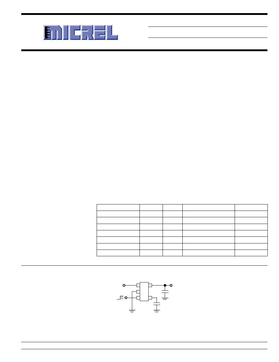
Typical Application
1
5
2
3
4
C
OUT
C
BYP
Enable
Shutdown
EN
V
OUT
(optional)
MIC5247-x.xBM5
EN (pin 3) may be
connected directly
to IN (pin 1).
V
IN
Ultra-Low-Noise Regulator Application
MIC5247
150mA Low-Voltage
µ
Cap Linear Regulator
Features
∑ Ultra-low-noise
∑ Low voltage outputs
∑ Load independent, ultra-low ground current: 85
µ
A
∑ 150mA output current
∑ Current limiting
∑ Thermal Shutdown
∑ Tight load and line regulation
∑ "Zero" off-mode current
∑ Stability with low-ESR capacitors
∑ Fast transient response
∑ Logic-controlled enable input
Applications
∑ Cellular phones and pagers
∑ Cellular accessories
∑ Battery-powered equipment
∑ Laptop, notebook, and palmtop computers
∑ PCMCIA V
CC
and V
PP
regulation/switching
∑ Consumer/personal electronics
∑ SMPS post-regulator/DC-to-DC modules
∑ High-efficiency linear power supplies
Micrel, Inc. ∑ 1849 Fortune Drive ∑ San Jose, CA 95131 ∑ USA ∑ tel + 1 (408) 944-0800 ∑ fax + 1 (408) 944-0970 ∑ http://www.micrel.com
IttyBitty is a trademark of Micrel, Inc.
MIC5247
Micrel
MIC5247
2
June 2003
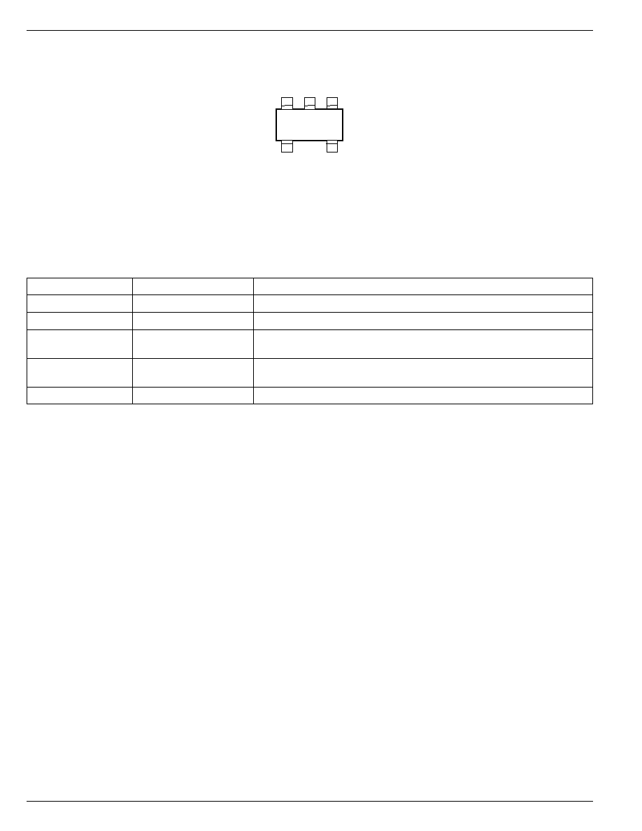
Pin Configuration
IN
OUT
BYP
EN
LUxx/
NUxx
1
3
4
5
2
GND
MIC5247-x.xBM5
MIC5247-x.xBD5
Pin Description
Pin Number
Pin Name
Pin Function
1
IN
Supply Input
2
GND
Ground
3
EN
Enable/Shutdown (Input): CMOS compatible input. Logic high = enable;
logic low = shutdown. Do not leave open.
4
BYP
Reference Bypass: Connect external 0.01pF capacitor to GND to reduce
output noise. May be left open.
5
OUT
Regulator Output
MIC5247
Micrel
June 2003
3
MIC5247
Electrical Characteristics
(Note 4)
V
IN
= V
OUT
+ 1.0V; V
IN
= V
EN
; I
OUT
= 100
µ
A; T
J
= 25
∞
C, bold values indicate ≠40
∞
C
T
J
+125
∞
C; unless noted.
Symbol
Parameter
Conditions
Min
Typical
Max
Units
V
O
Output Voltage Accuracy
I
OUT
= 0mA
≠1
1
%
≠2
2
%
V
LNR
Line Regulation
V
IN
= 2.7V to 6V
≠0.3
+0.3
%/V
V
LDR
Load Regulation
I
OUT
= 0.1mA to 150mA, Note 5
2
3
%
Load Regulation for 1.5V only
I
OUT
= 0.1mA to 150mA, V
OUT
= 1.5V
3
4
%
V
IN
≠ V
OUT
Dropout Voltage
I
OUT
= 150mA, Note 6
150
mV
I
Q
Quiescent Current
V
EN
0.4V (shutdown)
0.2
1
µ
A
I
GND
Ground Pin Current, Note 7
I
OUT
= 0mA
85
150
µ
A
I
OUT
= 150mA
85
150
µ
A
PSRR
Power Supply Rejection
f
1kHz
50
dB
I
LIM
Current Limit
V
OUT
= 0V
160
300
mA
e
n
Output Voltage Noise
C
OUT
= 10
µ
F, C
BYP
= 0.01
µ
F,
30
µ
Vrms
f = 10Hz to 100kHz
Enable Input
V
IL
Enable Input Logic-Low Voltage
V
IN
= 2.7V to 5.5V, regulator shutdown
0.8
0.4
V
V
IH
Enable Input Logic-High Voltage
V
IN
= 2.7V to 5.5V, regulator enabled
1.6
1
V
I
EN
Enable Input Current
V
IL
0.4V
0.01
µ
A
V
IH
1.6V
0.01
µ
A
Shutdown Resistance Discharge
500
Thermal Protection
Thermal Shutdown Temperature
150
∞
C
Thermal Shutdown Hysteresis
10
∞
C
Note 1.
Exceeding the absolute maximum rating may damage the device.
Note 2.
The device is not guaranteed to function outside its operating rating.
Note 3.
Devices are ESD sensitive. Handling precautions recommended.
Note 4.
Specification for packaged product only.
Note 5.
Regulation is measured at constant junction temperature using low duty cycle pulse testing. Parts are tested for load regulation in the load
range from 0.1mA to 150mA. Changes in output voltage due to heating effects are covered by the thermal regulation specification.
Note 6.
Dropout voltage is defined as the input to output differential at which the output voltage drops 2% below its nominal value measured a1V
differential. For outputs below 2.7V, dropout voltage is the input-to-output voltage differential with the minimum input voltage 2.7V. Minimum
input operating voltage is 2.7V.
Note 7.
Ground pin current is the regulator quiescent current plus pass transistor base current. The total current drawn from the supply is the sum of
the load current plus the ground pin current.
Absolute Maximum Ratings
(Note 1)
Supply Input Voltage (V
IN
) .................................. 0V to +7V
Enable Input Voltage (V
EN
) .................................. 0V to V
IN
Junction Temperature (T
J
) ...................................... +150
∞
C
Storage Temperature ............................... ≠65
∞
C to +150
∞
C
Lead Temperature (soldering, 5 sec.) ....................... 260
∞
C
ESD, Note 3
Operating Ratings
(Note 2)
Input Voltage (V
IN
) ......................................... +2.7V to +6V
Enable Input Voltage (V
EN
) .................................. 0V to V
IN
Junction Temperature (T
J
) ....................... ≠40
∞
C to +125
∞
C
Thermal Resistance (
JA
) ...................................... 235
∞
C/W
MIC5247
Micrel
MIC5247
4
June 2003
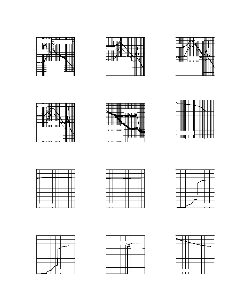
0
10
20
30
40
50
60
70
80
90
1x10
1
1x10
2
1x10
3
1x10
4
1x10
5
1x10
6
PSRR (dB)
FREQUENCY (Hz)
Power Supply Rejection Ratio
C
BYP
= 0
C
BYP
= 0.01
µ
F
C
BYP
= 1
µ
F
I
L
= 100
µ
A
V
IN
= 3.4V
V
OUT
= 2.4V
C
OUT
= 10
µ
F Ceramic
0
10
20
30
40
50
60
70
1x10
1
1x10
2
1x10
3
1x10
4
1x10
5
1x10
6
PSRR (dB)
FREQUENCY (Hz)
Power Supply Rejection Ratio
C
BYP
= 0
0.01
µ
F
1
µ
F
I
L
= 50mA
V
IN
= 3.4V
V
OUT
= 2.4V
C
OUT
=10
µ
F Ceramic
0
10
20
30
40
50
60
1x10
1
1x10
2
1x10
3
1x10
4
1x10
5
1x10
6
PSRR (dB)
FREQUENCY (Hz)
Power Supply Rejection Ratio
C
BYP
= 0
0.01
µ
F
1
µ
F
I
L
= 100mA
V
IN
= 3.4V
V
OUT
= 2.4V
C
OUT
= 10
µ
F Ceramic
0
20
40
60
80
100
-40
-10
20
50
80
110 140
GROUND CURRENT (
µ
A)
TEMPERATURE (
∞
C)
Ground Pin Current
I
LOAD
= 100
µ
A
0
20
40
60
80
100
0
1
2
3
4
GROUND CURRENT (
µ
A)
INPUT VOLTAGE (V)
Ground Pin Current
I
LOAD
= 100
µ
A
0
20
40
60
80
100
0
1
2
3
4
GROUND CURRENT (
µ
A)
INPUT VOLTAGE (V)
Ground Pin Current
I
LOAD
= 150mA
0
1
2
3
0
1
2
3
4
VOLTAGE OUT (V)
INPUT VOLTAGE (V)
Dropout Characteristics
I
LOAD
= 100
µ
A
I
LOAD
=
150mA
0
100
200
300
400
500
-40
-10
20
50
80
110 140
SHORT CIRCUIT CURRENT (mA)
TEMPERATURE (
∞
C)
Short Circuit Current
vs. Temperature
VOUT = 0
0
10
20
30
40
50
60
1x10
1
1x10
2
1x10
3
1x10
4
1x10
5
1x10
6
PSRR (dB)
FREQUENCY (Hz)
Power Supply Rejection Ratio
C
BYP
= 0
0.01
µ
F
1
µ
F
I
L
= 150mA
V
IN
= 3.4V
V
OUT
= 2.4V
C
OUT
= 10
µ
F Ceramic
0
20
40
60
80
100
-40
-10
20
50
80
110 140
GROUND CURRENT (
µ
A)
TEMPERATURE (
∞
C)
Ground Pin Current
I
LOAD
= 150mA
Typical Characteristics
1x10
-8
1x10
-7
1x10
-6
1x10
-5
1x10
1
1x10
2
1x10
3
1x10
4
1x10
5
1x10
6
OUTPUT SPECTRAL NOISE DENSITY (
µ
V/rt Hz)
FREQUENCY (Hz)
Noise Performance
C
BYP
= 0
C
BYP
= 0.01
µ
F
V
IN
= 2.8V
V
OUT
= 1.8V
C
OUT
= 4.7
µ
F
I
LOAD
= 50mA
70
71
72
73
74
75
1x10
-1
1x10
0
1x10
1
1x10
2
1x10
3
GROUND CURRENT (
µ
A)
OUTPUT CURRENT (mA)
Ground Current
vs. Output Current
V
IN
= V
OUT
+ 1

MIC5247
Micrel
June 2003
5
MIC5247
2.3
2.4
2.5
-40
-10
20
50
80
110 140
OUTPUT VOLTAGE (V)
TEMPERATURE (
∞
C)
Output Voltage
vs. Temperature
I
LOAD
= 100
µ
A
0
50
100
150
200
1x10
-5
1x10
-4
1x10
-3
1x10
-2
1x10
-1
1x10
0
1x10
1
TIME (
µ
s)
BYPASS CAPACITOR (
µ
F)
Turn-On Time
vs. Bypass Capacitance
Rise Time
Prop Delay
C
OUT
= 10
µ
F
I
LOAD
= 100mA