January 2002
1
MIC5249
MIC5249
Micrel
MIC5249
300mA
µ
Cap LDO with Programmable Power-On Reset Delay
Advance Information
General Description
The MIC5249 is an efficient, precise 300mA CMOS voltage
regulator with power-on reset delay which can be imple-
mented via an external capacitor. It offers 1% initial accuracy,
extremely-low-dropout voltage (typically 400mV @ 300mA),
and low ground current (typically 85
µ
A) over load.
Designed specifically for noise-critical applications in hand-
held or battery-powered devices, the MIC5249 comes
equipped with a noise reduction feature to filter the output
noise via an external capacitor. Other features of the MIC5249
include a logic compatible enable pin, current limit, thermal
shutdown, ultra-fast transient response, and an active clamp
to speed up device turnoff.
The MIC5249 also works with low-ESR ceramic capacitors,
reducing the amount of board space necessary for power
applications, critical in hand-held wireless devices.
The MIC5249 is available in the MSOP-8 package.
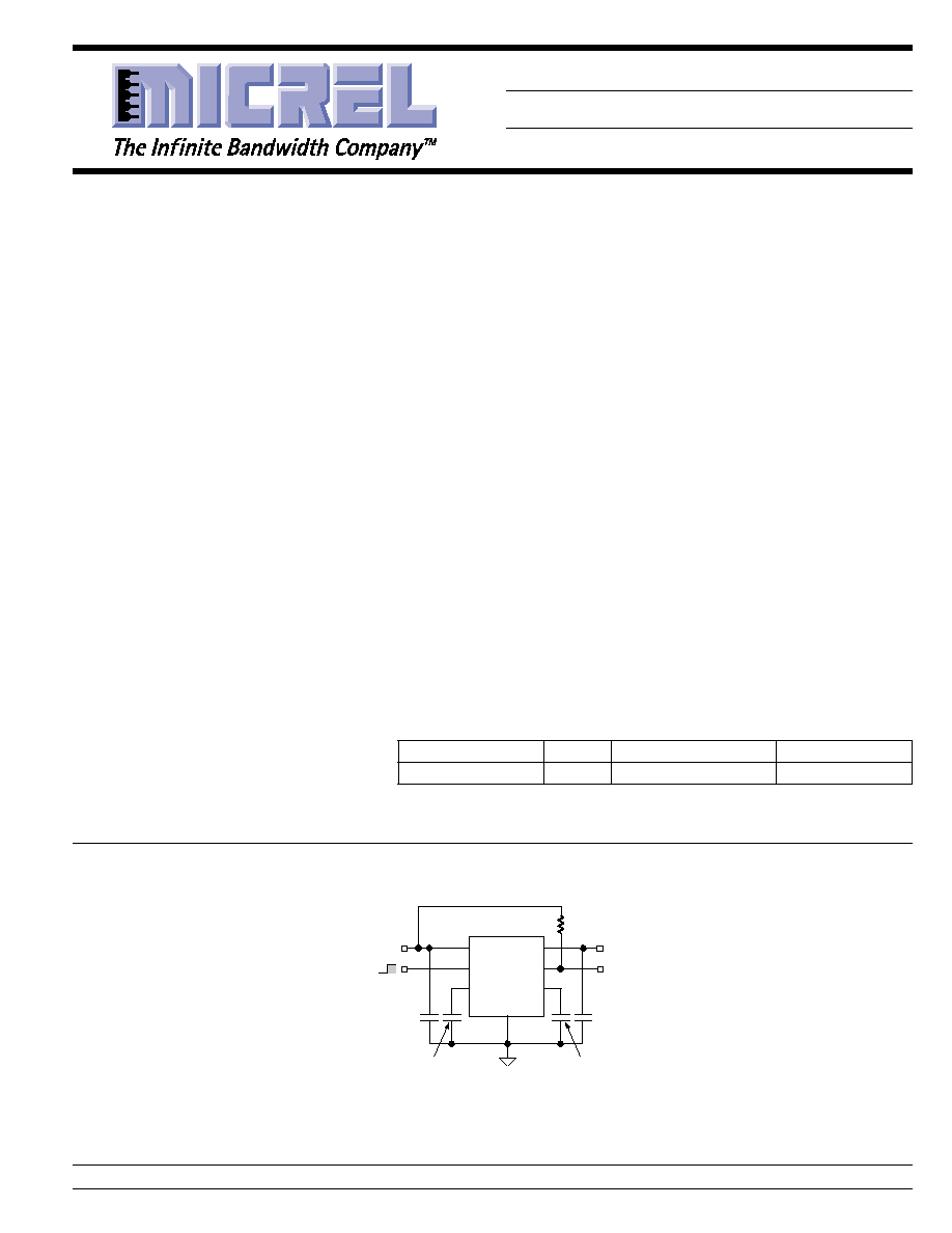
Typical Application
MIC5249-x.xBMM
IN
OUT
GND
V
IN
RESET
C
OUT
=2.2
µ
F
Ceramic
C
BYP
=0.01
µ
F
Sets the delay for
the RESET output
C
AD
=1.0
µ
F
Ceramic
V
OUT
EN
DELAY
RESET
CBYP
ENABLE
SHUTDOWN
Ultra-Low-Noise Application
Features
∑ 300mA output current
∑ High PSRR: 65dB@120Hz
∑ Stable with ceramic output capacitor
∑ Power-on RESET Output with adjustable delay time
∑ High output accuracy:
+1.0% initial accuracy
+2.0% over temperature
∑ Low dropout voltage of 400mV @ 300mA
∑ Low quiescent current: 85
µ
A
∑ Zero current shutdown mode
∑ Thermal shutdown protection
∑ Current-limit protection
∑ Tiny MSOP-8 package
Applications
∑ Cellular phones
∑ PDAs
∑ Fiber optic modules
Micrel, Inc. ∑ 1849 Fortune Drive ∑ San Jose, CA 95131 ∑ USA ∑ tel + 1 (408) 944-0800 ∑ fax + 1 (408) 944-0970 ∑ http://www.micrel.com
Ordering Information
Part Number
Voltage
Junction Temp. Range
Package
MIC5249-2.85BMM
2.85V
≠40
∞
C to 125
∞
C
MSOP-8
Other voltages available. Contact Micrel for details.
MIC5249
Micrel
MIC5249
2
January 2002
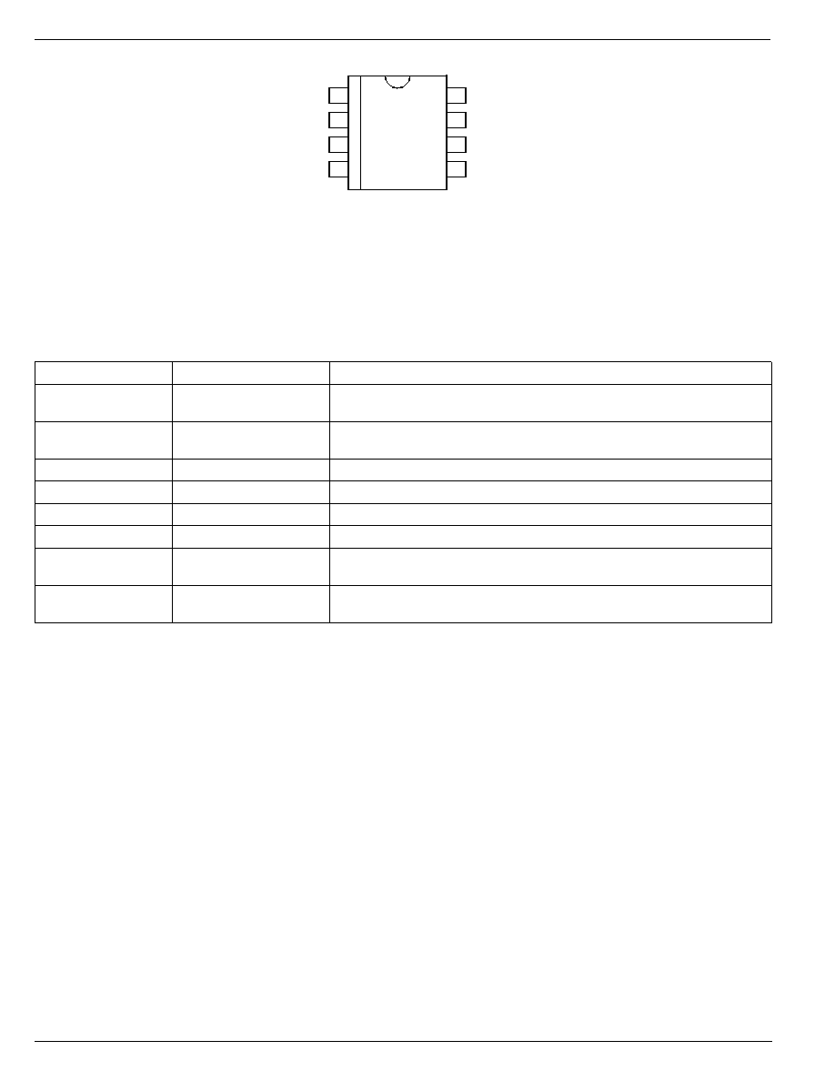
Pin Description
Pin No.
Pin Name
Pin Function
1
CBYP
Reference Bypass: Connect external 0.01
µ
F capacitor to GND to reduce
output noise. May be left open.
2
DELAY
Delay Set Input: Connect external capacitor to GND to set the delay of the
Error Flag.
3
GND
Ground
4
VIN
Supply Input
5
VOUT
Regulator Output
6
NC
No Connect.
7
RESET
RESET Output: Open-drain output. Active low indicates an output
undervoltage condition.
8
ENABLE
Enable Input: CMOS compatible input. Logic high = enable; Logic low =
shutdown. Do not leave open.
Pin Configuration
1
CBYP
DELAY
GND
VIN
8
ENABLE
RESET
NC
VOUT
7
6
5
2
3
4
8-pin MSOP (MM)
January 2002
3
MIC5249
MIC5249
Micrel
Electrical Characteristics
V
IN
= V
OUT
+1.0V; C
OUT
= 1.0
µ
F, I
OUT
= 100
µ
A; T
J
= 25
∞
C, bold values indicate ≠40
∞
C to + 125
∞
C; unless noted.
Parameter
Conditions
Min
Typ
Max
Units
Output Voltage Accuracy
Variation from nominal V
OUT
≠1.0
+1.0
%
≠2.0
+2.0
%
Line Regulation
V
IN
= V
OUT
+1V to 6V
≠0.3
0.02
+0.3
%/V
Load Regulation
I
OUT
= 0.1mA to 300mA
1.5
3.0
%
Dropout Voltage
I
OUT
= 100
µ
A
1
mV
I
OUT
= 150mA
175
225
mV
275
mV
I
OUT
= 300mA
400
500
mV
600
mV
Ground Pin Current
I
OUT
= 0mA
85
150
µ
A
I
OUT
= 300mA
100
175
µ
A
Ground Pin Current in Shutdown
V
EN
< 0.4V (Regulator OFF)
0.35
1
µ
A
Ripple Rejection
f = 120Hz, C
OUT
= 2.2
µ
F
65
dB
Current Limit
V
OUT
= 0V
330
550
mA
Enable Input
Enable Input Voltage
Logic Low (Regulator Shutdown)
0.4
V
Logic High (Regulator Enabled)
1.6
V
Enable Input Current
V
IL
< 0.4V (Regulator Shutdown)
0.01
µ
A
V
IH
> 1.6V (Regulator Enabled)
0.01
µ
A
Delay Input
Delay Pin Current Source
0.55
1
µ
A
Delay Pin Threshold Voltage
Threshold for RESET = Logic High
1.40
V
RESET Output
V
TH
Low Threshold, % of V
OUT
(Flag ON)
89
%
High Threshold, % of V
OUT
(Flag OFF)
93
%
V
OL
RESET Output Logic - Low Voltage; I
RESET
= 100
µ
A
0.020
0.1
V
output in fault condition
I
RESET
Flag Leakage Current, Flag OFF
0.01
µ
A
Note 1:
Exceeding maximum rating may damage the device.
Note 2:
The device is not guaranteed to work outside its operating rating.
Note 3:
The maximum allowable power dissipation of any T
A
(ambient temperature) is P
D(max)
= T
J(max)
- TA) /
JA
. Exceeding the maximum
allowable power dissipation will result in excessive die temperature, and the regulator will go into thermal shutdown.
Note 4.
Devices are ESD sensitive. Handling precautions recommended. Human body model, 1.5k in series with 100pF.
Absolute Maximum Ratings
(Note 1)
Supply Input Voltage (V
IN
) .................................... 0V to 7V
Power Dissipation (P
D
) ............... Internally Limited, Note 3
Junction Temperature .............................. ≠40
∞
C to +125
∞
C
Lead Temperature (soldering, 5 sec.) ....................... 260
∞
C
Storage Temperature (T
S
) ......................... ≠65
∞
C to 150
∞
C
ESD Rating, Note 4
Operating Ratings
(Note 2)
Supply Input Voltage (V
IN
) ................................. 2.7V to 6V
Enable Input Voltage (V
EN
) .................................. 0V to V
IN
Junction Temperataure (T
J
) ..................... ≠40
∞
C to +125
∞
C
Package Thermal Resistance
MSOP-8 (
JA
) .................................................... 200
∞
C/W
MIC5249
Micrel
MIC5249
4
January 2002
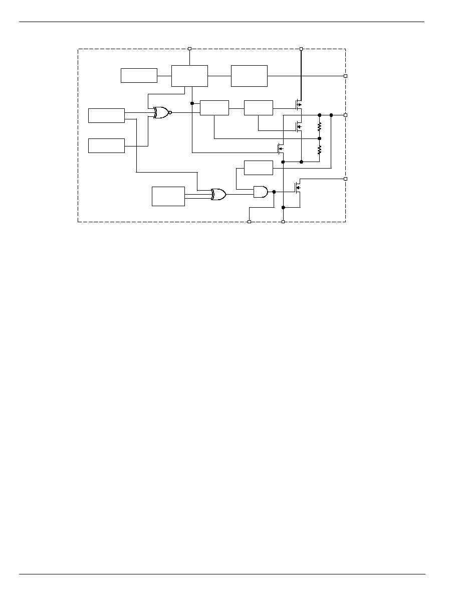
Functional Diagram
Out of
regulation
Current
Amplifier
Error
Amplifier
Thermal
Sensor
V
REF
Startup/
Shutdown
Control
EN
Quickstart/
Noise
Cancellation
IN
BYP
OUT
RESET
GND
Delay
Overcurrent
Dropout
Detection
Undervoltage
Lockout

January 2002
5
MIC5249
MIC5249
Micrel
Applications Information
Enable/Shutdown
The MIC5249 comes with an active-high enable pin that
allows the regulator to be disabled. Forcing the enable pin low
disables the regulator and sends it into a "zero" off-mode-
current state. In this state, current consumed by the regulator
goes nearly to zero. Forcing the enable pin high enables the
output voltage. This part is CMOS and the enable pin cannot
be left floating; a floating enable pin may cause an indetermi-
nate state on the output.
Input Capacitor
The MIC5249 is a high performance, high bandwidth device.
Therefore, it requires a well-bypassed input supply for opti-
mal performance. A 1.0
µ
F capacitor is required from the input
to ground to provide stability. Low-ESR ceramic capacitors
provide optimal performance at a minimum of space. Addi-
tional high-frequency capacitors such as small valued NPO
dielectric type capacitors help to filter out high frequency
noise and are good practice in any RF based circuit.
Output Capacitor
The MIC5249 requires an output capacitor for stability. The
design requires 2.2
µ
F or greater on the output to maintain
stability. The design is optimized for use with low-ESR
ceramic chip capacitors. High ESR capacitors may cause
high frequency oscillation. The maximum recommended
ESR is 300m
. The output capacitor can be increased, but
performance has been optimized for a 2.2
µ
F ceramic output
capacitor and does not improve significantly with larger
capacitance.
X7R/X5R dielectric-type ceramic capacitors are recom-
mended because of their temperature performance. X7R-
type capacitors change capacitance by 15% over their oper-
ating temperature range and are the most stable type of
ceramic capacitors. Z5U and Y5V dielectric capacitors change
value by as much as 50% and 60% respectively over their
operating temperature ranges. To use a ceramic chip capaci-
tor with Y5V dielectric, the value must be much higher than an
X7R ceramic capacitor to ensure the same minimum capaci-
tance over the equivalent operating temperature range.
Delay Pin Input
The power-on reset function can be implemented on the
MIC5249 by adding an external capacitor from the delay pin
to ground. This external capacitor sets the delay time (T
DELAY
)
of the RESET output. The capacitor value required can be
easily calculated using the formula:
C
T
I
V
DELAY
DELAY
DELAY
DELAY
=
◊
where I
DELAY
is 0.55
µ
A and the V
DELAY
is 1.4V. When no
capacitor is used, there will be no delay and the POR output
acts like a standard error FLAG output.
Reset Output
The RESET output of the MIC5249 provides the power-on
reset signal based on the capacitor from the DELAY pin to
ground when input power is applied to the regulator. The
reset signal stays low for a pre-set time period after power is
applied to the regulator, and then goes high (see Timing
Diagram).
The reset output is an active-low, open-drain output that
drives low when a fault condition AND an undervoltage
detection occurs. Internal circuitry intelligently monitors
overcurrent, overtemperature and dropout conditions and
Ors these outputs together to indicate some fault condition.
The output of that OR gate is ANDed with an output voltage
monitor that detects an undervotlage condition. The output
drives an open-drain transistor to indicate a fault. This pre-
vents chattering or inadvertent triggering of the reset. The
reset must be pulled up using a resistor form the RESET pin
to either the input or the output.
Bypass Pin Input
A bypass capacitor is required from the noise bypass pin to
ground to reduce output voltage noise. The capacitor by-
passes the internal reference. A 0.01
µ
F capacitor is recom-
mended for applications that require low-noise outputs. The
bypass capacitor can be increased, further reducing noise
and improving PSRR. Turn-on time increases slightly with
respect to bypass capacitance. A unique quick-start circuit
allows the MIC5249 to drive a large capacitor on the bypass
pin without significantly slowing the turn-on time. Refer to the
"Typical Characteristics" section for performance with differ-
ent bypass capacitors.
Active Shutdown
The MIC5249 also features an active shutdown clamp, which
is an N-channel MOSFET that turns on when the device is
disabled. This allows the output capacitor and load to dis-
charge, de-energizing the load.
No-Load Stability
The MIC5249 will remain stable and in regulation with no load
unlike many other voltage regulators. This is especially
important in CMOS RAM keep-alive application.