MIC5250
Micrel
March 2000
1
MIC5250
General Description
The MIC5250 is an efficient, precise dual CMOS voltage
regulator optimized for ultra-low-noise applications. The
MIC5250 offers better than 1% initial accuracy, extremely low
dropout voltage (typically 150mV at 150mA) and constant
ground current over load (typically 100
µ
A). The MIC5250
provides a very-low-noise output, ideal for RF applications
where quiet voltage sources are required. A noise bypass pin
is also available for further reduction of output noise.
Designed specifically for hand-held and battery-powered
devices, the MIC5250 provides TTL logic compatible enable
pins. When disabled, power consumption drops nearly to
zero.
The MIC5250 also works with low-ESR ceramic capacitors,
reducing the amount of board space necessary for power
applications, critical in hand-held wireless devices.
Key features include current limit, thermal shutdown, push-
pull outputs for faster transient response, and active clamps
to speed up device turnoff. Available in the 10-lead MSOP
(micro-shrink-outline package), the MIC5250 also offers a
range of fixed output voltages.
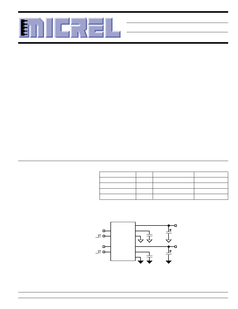
Typical Application
C
BYPB
(optional)
C
OUTB
INA
OUTA
BYPA
GNDA
OUTB
BYPB
GNDB
ENA
INB
ENB
3.3V
V
INA
V
INB
3.3V
MIC5250-3.3BMM
C
BYPA
(optional)
C
OUTA
ENABLE
SHUTDOWN
ENABLE
SHUTDOWN
ENA may be connected directly to INA.
ENB may be connected directly to INB.
GNDA and GND B may be connected to
isolated grounds or the same ground.
10
1
3
8
4
6
2
9
7
5
Dual Ultra-Low-Noise Regulator Circuit
MIC5250
Dual 150mA
µ
Cap CMOS LDO Regulator
Preliminary Information
Features
∑ Ultralow dropout--100mV @ 100mA
∑ Ultralow noise--30
µ
V(rms)
∑ Stability with ceramic, tantalum, or aluminum electrolytic
capacitors
∑ Load independent, ultralow ground current
∑ 150mA output current
∑ Current limiting
∑ Thermal Shutdown
∑ Tight load and line regulation
∑ "Zero" off-mode current
∑ Fast transient response
∑ TTL-Logic-controlled enable input
Applications
∑ Cellular phones and pagers
∑ Cellular accessories
∑ Battery-powered equipment
∑ Laptop, notebook, and palmtop computers
∑ PCMCIA V
CC
and V
PP
regulation/switching
∑ Consumer/personal electronics
∑ SMPS post-regulator/dc-to-dc modules
∑ High-efficiency linear power supplies
Micrel, Inc. ∑ 1849 Fortune Drive ∑ San Jose, CA 95131 ∑ USA ∑ tel + 1 (408) 944-0800 ∑ fax + 1 (408) 944-0970 ∑ http://www.micrel.com
Ordering Information
Part Number
Voltage
Junction Temp. Range
Package
MIC5250-2.7BMM
2.7V
≠40
∞
C to +125
∞
C
10-lead MSOP
MIC5250-2.8BMM
2.8V
≠40
∞
C to +125
∞
C
10-lead MSOP
MIC5250-3.0BMM
3.0V
≠40
∞
C to +125
∞
C
10-lead MSOP
MIC5250-3.3BMM
3.3V
≠40
∞
C to +125
∞
C
10-lead MSOP
Other voltages available. Contact Micrel for details.

MIC5250
Micrel
MIC5250
2
March 2000
Pin Configuration
1
BYPA
ENA
GNDA
BYPB
ENB
10 OUTA
INA
OUTB
INB
GNDB
9
8
7
6
2
3
4
5
MIC5250-x.xBMM
Absolute Maximum Ratings
(Note 1)
Supply Input Voltage (V
IN
) .................................. 0V to +7V
Enable Input Voltage (V
EN
) ................................. 0V to +7V
Junction Temperature (T
J
) ...................................... +150
∞
C
Storage Temperature ............................... ≠65
∞
C to +150
∞
C
Lead Temperature (soldering, 5 sec.) ....................... 260
∞
C
ESD, Note 3
Operating Ratings
(Note 2)
Input Voltage (V
IN
) ......................................... +2.7V to +6V
Enable Input Voltage (V
EN
) .................................. 0V to V
IN
Junction Temperature (T
J
) ....................... ≠40
∞
C to +125
∞
C
Thermal Resistance
(
JA
) ...................................... 200
∞
C/W
Pin Description
Pin Number
Pin Name
Pin Function
9 / 7
INA / B
Supply Input*
3 / 6
GNDA / B
Ground*
2 / 4
ENA / B
Enable/Shutdown (Input): CMOS compatible input. Logic high = enable;
logic low = shutdown. Do not leave open.
1 / 4
BYPA / B
Reference Bypass: Connect external 0.01
µ
F capacitor to GND to reduce
output noise. May be left open.
10 / 8
OUTA / B
Regulator Output
* Supply inputs and grounds are fully isolated.

MIC5250
Micrel
March 2000
3
MIC5250
Electrical Characteristics
Each regulator: V
IN
= V
OUT
+ 1V, V
EN
= V
IN;
I
OUT
= 100
µ
A; T
J
= 25
∞
C, bold values indicate ≠40
∞
C
T
J
+125
∞
C; unless noted.
Symbol
Parameter
Conditions
Min
Typical
Max
Units
V
O
Output Voltage Accuracy
I
OUT
= 0mA
≠1
1
%
≠2
2
%
V
LNR
Line Regulation
V
IN
= V
OUT
+ 0.1V to 6V
≠0.3
0
0.3
%/V
V
LDR
Load Regulation
I
OUT
= 0.1mA to 150mA, Note 4
2.0
3.0
%
V
IN
≠ V
OUT
Dropout Voltage, Note 5
I
OUT
= 100
µ
A
1.5
5
mV
I
OUT
= 50mA
50
85
mV
I
OUT
= 100mA
100
150
mV
I
OUT
= 150mA
150
200
mV
250
mV
I
Q
Quiescent Current
V
EN
0.4V (shutdown)
0.2
1
µ
A
I
GND
Ground Pin Current, Note 6
I
OUT
= 0mA
100
150
µ
A
I
OUT
= 150mA
100
µ
A
PSRR
Power Supply Rejection
f = 120Hz, C
OUT
= 10
µ
F, C
BYP
= 0.01
µ
F
50
dB
I
LIM
Current Limit
V
OUT
= 0V
160
300
mA
e
n
Output Voltage Noise
C
OUT
= 10
µ
F, C
BYP
= 0.01
µ
F,
30
µ
V(rms)
f = 10Hz to 100kHz
Enable Input
V
IL
Enable Input Logic-Low Voltage
V
IN
= 2.7V to 5.5V, regulator shutdown
0.8
0.4
V
V
IH
Enable Input Logic-High Voltage
V
IN
= 2.7V to 5.5V, regulator enabled
2.0
1
V
I
EN
Enable Input Current
V
IL
0.4V
0.17
µ
A
V
IH
2.0V
1.5
µ
A
Shutdown Resistance Discharge
500
Thermal Protection
Thermal Shutdown Temperature
150
∞
C
Thermal Shutdown Hysteresis
10
∞
C
Note 1.
Exceeding the absolute maximum rating may damage the device.
Note 2.
The device is not guaranteed to function outside its operating rating.
Note 3.
Devices are ESD sensitive. Handling precautions recommended.
Note 4.
Regulation is measured at constant junction temperature using low duty cycle pulse testing. Parts are tested for load regulation in the load
range from 0.1mA to 150mA. Changes in output voltage due to heating effects are covered by the thermal regulation specification.
Note 5.
Dropout Voltage is defined as the input to output differential at which the output voltage drops 2% below its nominal value measured at 1V
differential.
Note 6.
Ground pin current is the regulator quiescent current. The total current drawn from the supply is the sum of the load current plus the ground
pin current.
MIC5250
Micrel
MIC5250
4
March 2000
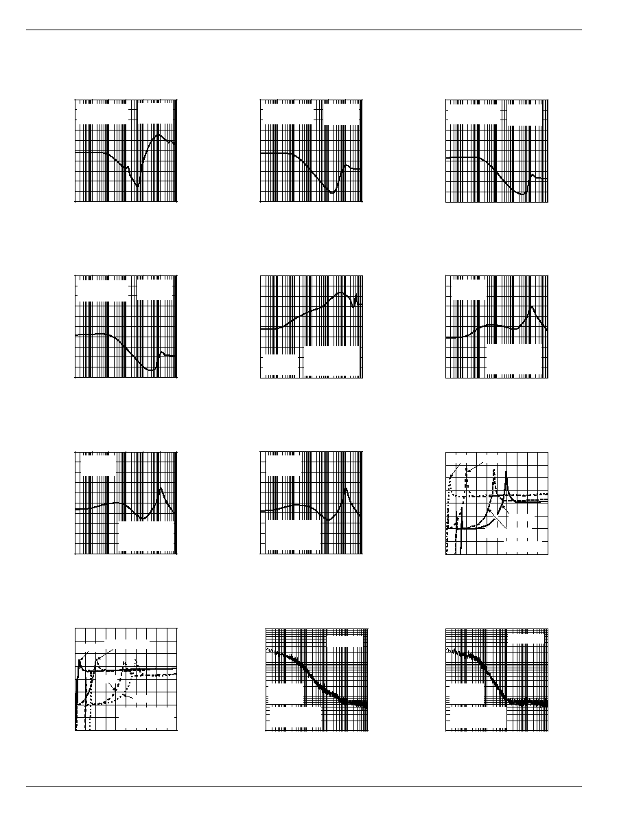
0
20
40
60
80
100
1E+1 1E+2 1E+3 1E+4 1E+5 1E+6 1E+7
PSRR (dB)
FREQUENCY (Hz)
Power Supply
Rejection Ratio
I
OUT
= 100
µ
A
C
OUT
= 1
µ
F tant
V
IN
= 4V
V
OUT
= 3V
10
100
1k
10k 100k 1M 10M
0
20
40
60
80
100
1E+1 1E+2 1E+3 1E+4 1E+5 1E+6 1E+7
PSRR (dB)
FREQUENCY (Hz)
Power Supply
Rejection Ratio
I
OUT
= 10mA
C
OUT
= 1
µ
F tant
V
IN
= 4V
V
OUT
= 3V
10
100
1k
10k 100k 1M 10M
0
20
40
60
80
100
1E+1 1E+2 1E+3 1E+4 1E+5 1E+6 1E+7
PSRR (dB)
FREQUENCY (Hz)
Power Supply
Rejection Ratio
I
OUT
= 100mA
C
OUT
= 1
µ
F tant
V
IN
= 4V
V
OUT
= 3V
10
100
1k
10k 100k 1M 10M
0
20
40
60
80
100
1E+1 1E+2 1E+3 1E+4 1E+5 1E+6 1E+7
PSRR (dB)
FREQUENCY (Hz)
Power Supply
Rejection Ratio
I
OUT
= 150mA
C
OUT
= 1
µ
F tant
V
IN
= 4V
V
OUT
= 3V
10
100
1k
10k 100k 1M 10M
0
20
40
60
80
100
1E+1 1E+2 1E+3 1E+4 1E+5 1E+6 1E+7
PSRR (dB)
FREQUENCY (Hz)
Power Supply
Rejection Ratio
I
OUT
= 100
µ
A
C
OUT
= 10
µ
F cer.
C
BYP
= 0.01
µ
F
V
IN
= 4V
V
OUT
= 3V
10
100
1k
10k 100k 1M 10M
0
20
40
60
80
100
1E+1 1E+2 1E+3 1E+4 1E+5 1E+6 1E+7
PSRR (dB)
FREQUENCY (Hz)
Power Supply
Rejection Ratio
I
OUT
= 10mA
C
OUT
= 10
µ
F cer.
C
BYP
= 0.01
µ
F
V
IN
= 4V
V
OUT
= 3V
10
100
1k
10k 100k 1M 10M
0
20
40
60
80
100
1E+1 1E+2 1E+3 1E+4 1E+5 1E+6 1E+7
PSRR (dB)
FREQUENCY (Hz)
10
Power Supply
Rejection Ratio
I
OUT
= 100mA
C
OUT
= 10
µ
F cer.
C
BYP
= 0.01
µ
F
V
IN
= 4V
V
OUT
= 3V
100
1k
10k 100k 1M 10M
0
20
40
60
80
100
1E+1 1E+2 1E+3 1E+4 1E+5 1E+6 1E+7
PSRR (dB)
FREQUENCY (Hz)
Power Supply
Rejection Ratio
I
OUT
= 150mA
C
OUT
= 10
µ
F cer.
C
BYP
= 0.01
V
IN
= 4V
V
OUT
= 3V
10
100
1k
10k 100k 1M 10M
0
10
20
30
40
50
60
70
80
0
200
400
600
800
1000
RIPPLE REJECTION (dB)
VOLTAGE DROP (mV)
Power Supply Ripple Rejection
vs. Voltage Drop
I
OUT
= 100mA
10mA
100
µ
A
C
OUT
= 1
µ
F
150mA
0
10
20
30
40
50
60
70
80
0
200
400
600
800
1000
RIPPLE REJECTION (dB)
VOLTAGE DROP (mV)
Power Supply Ripple Rejection
vs. Voltage Drop
I
OUT
= 100mA
10mA
100
µ
A
C
OUT
= 10
µ
F cer.
C
BYP
= 0.01
µ
F
100mA
0.01
0.1
1
10
1E+1 1E+2 1E+3 1E+4 1E+5 1E+6
NOISE (
µ
V/
Hz)
FREQUENCY (Hz)
Noise Performance
10
100
1k
10k
100k
1M
I
L
= 100
µ
A
V
IN
= 4V
V
OUT
= 3V
C
OUT
= 1
µ
F cer.
C
BYP
= 0.01
µ
F
0.01
0.1
1
10
1E+1 1E+2 1E+3 1E+4 1E+5 1E+6
NOISE (
µ
V/
Hz)
FREQUENCY (Hz)
Noise Performance
10
100
1k
10k
100k
1M
I
L
= 100
µ
A
V
IN
= 4V
V
OUT
= 3V
C
OUT
= 10
µ
F cer.
C
BYP
= 0.01
µ
F
Typical Characteristics
MIC5250
Micrel
March 2000
5
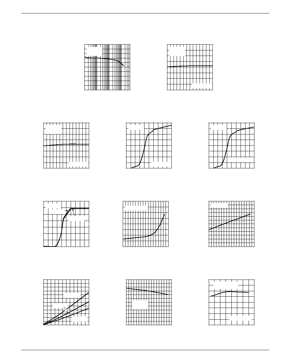
MIC5250
85
90
95
0.1
1
10
100
500
QUIESCENT CURRENT (
µ
A)
LOAD CURRENT (mA)
Ground Pin Current
V
IN
= 4V
V
OUT
= 3V
0
50
100
150
200
-40 -20
0
20
40
60
80 100
QUIESCENT CURRENT (
µ
A)
TEMPERATURE (
∞
C)
Ground Pin Current
V
IN
= 4V
V
OUT
= 3V
I
OUT
= 100
µ
A
50
75
100
125
150
-40 -20
0
20
40
60
80 100
QUIESCENT CURRENT (
µ
A)
TEMPERATURE (
∞
C)
Ground Pin Current
V
IN
= 4V
V
OUT
= 3V
I
OUT
= 150mA
0
25
50
75
100
0
1
2
3
4
5
QUIESCENT CURRENT (
µ
A)
INPUT VOLTAGE (V)
Ground Pin Current
V
OUT
= 3V
I
OUT
= 100
µ
A
0
25
50
75
100
0
1
2
3
4
5
QUIESCENT CURRENT (
µ
A)
INPUT VOLTAGE (V)
Ground Pin Current
V
OUT
= 3V
I
OUT
= 150mA
0
0.5
1.0
1.5
2.0
2.5
3.0
3.5
0
1
2
3
4
5
OUTPUT VOLTAGE (V)
INPUT VOLTAGE (V)
Dropout Characteristics
V
OUT
= 3V
R
L
= 30
R
L
= 30k
0
2
4
6
8
-40 -20 0 20 40 60 80 100120140
DROPOUT VOLTAGE (mV)
TEMPERATURE (
∞
C)
Dropout Voltage
I
LOAD
= 100
µ
A
0
50
100
150
200
250
300
-40 -20 0 20 40 60 80 100120140
DROPOUT VOLTAGE (mV)
TEMPERATURE (
∞
C)
Dropout Voltage
I
L
= 150mA
0
50
100
150
200
250
300
0
25
50
75
100 125 150
DROPOUT VOLTAGE (mV)
OUTPUT CURRENT (mA)
Dropout Voltage
T
A
= 25
∞
C
T
A
= -40
∞
C
T
A
= 125
∞
C
0
100
200
300
400
500
600
-40 -20 0 20 40 60 80 100120140
OUTPUT CURRENT (mA)
TEMPERATURE (
∞
C)
Short Circuit Current
V
IN
= 3.5V
V
EN
= 3V
2.85
2.90
2.95
3.00
3.05
-50
0
50
100
150
OUTPUT VOLTAGE (V)
TEMPERATURE (
∞
C)
Output Voltage
vs. Temperature
V
IN
= 4V
TYPICAL 3V DEVICE
I
LOAD
= 100
µ
A