MIC5252
Micrel
June 2003
1
MIC5252
General Description
The MIC5252 is an efficient, precise CMOS voltage regulator
optimized for ultra-low-noise applications. It offers 1% initial
accuracy, extremely low dropout voltage (135mV at 150mA)
and low ground current (typically 90
µ
A). The MIC5252 pro-
vides a very low noise output, ideal for RF applications where
a clean voltage source is required. The MIC5252 has a high
PSRR even at low supply voltages, critical for battery oper-
ated electronics. A noise bypass pin is also available for
further reduction of output noise.
Designed specifically for handheld and battery-powered de-
vices, the MIC5252 provides a TTL-logic-compatible enable
pin. When disabled, power consumption drops nearly to zero.
The MIC5252 also works with low-ESR ceramic capacitors,
reducing the amount of board space necessary for power
applications, critical in hand-held wireless devices.
Key features include current limit, thermal shutdown, faster
transient response, and an active clamp to speed up device
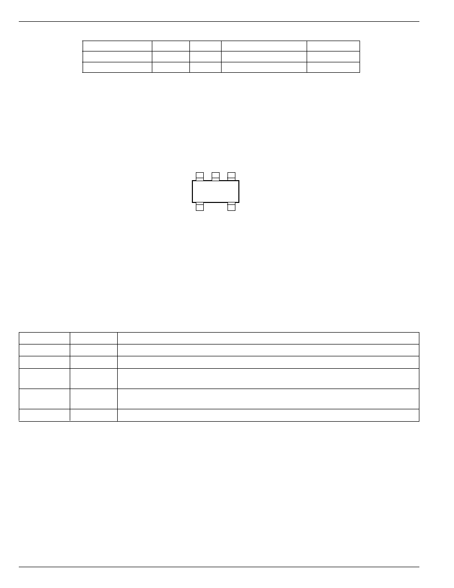
turn-off. The MIC5252 is available in the IttyBittyTM SOT-23-5
package in a wide range of output voltages.
Typical Application
C
OUT
= 1.0
µ
F
C
IN
= 1.0
µ
F
Ceramic
Ceramic
1
5
2
3
4
C
BYP
= 0.01
µ
F
Enable
Shutdown
EN
V
OUT
MIC5252-x.xBM5
EN (pin 3) may be
connected directly
to IN (pin 1).
V
IN
Ultra-Low-Noise Regulator Application
MIC5252
150mA High PSRR, Low Noise
µ
Cap CMOS LDO
Final Information
Features
∑ Input voltage range: 2.7V to 6.0V
∑ PSRR = 50dB @ V
O
+ 0.3V
∑ Ultralow output noise: 30
µ
V(rms)
∑ Stability with ceramic output capacitors
∑ Ultralow dropout: 135mV @ 150mA
∑ High output accuracy:
1.0% initial accuracy
2.0% over temperature
∑ Low quiescent current: 90
µ
A
∑ Tight load and line regulation
∑ TTL-Logic-controlled enable input
∑ "Zero" off-mode current
∑ Thermal shutdown and current limit protection
Applications
∑ Cellular phones and pagers
∑ Cellular accessories
∑ Battery-powered equipment
∑ Laptop, notebook, and palmtop computers
∑ Consumer/personal electronics
Micrel, Inc. ∑ 1849 Fortune Drive ∑ San Jose, CA 95131 ∑ USA ∑ tel + 1 (408) 944-0800 ∑ fax + 1 (408) 944-0970 ∑ http://www.micrel.com

MIC5252
Micrel
June 2003
3
MIC5252
Electrical Characteristics
V
IN
= V
OUT
+ 1V, V
EN
= V
IN;
I
OUT
= 100
µ
A; T
J
= 25
∞
C, bold values indicate ≠40
∞
C
T
J
+125
∞
C; unless noted.
Symbol
Parameter
Conditions
Min
Typical
Max
Units
V
O
Output Voltage Accuracy
I
OUT
= 100
µ
A
≠1
1
%
≠3
3
%
V
LNR
Line Regulation
V
IN
= V
OUT
+ 1V to 6V
0.02
0.05
%/V
V
LDR
Load Regulation
I
OUT
= 0.1mA to 150mA, Note 5
0.6
1.5
%
V
IN
≠ V
OUT
Dropout Voltage, Note 6
I
OUT
= 100
µ
A
0.1
5
mV
I
OUT
= 100mA
90
150
mV
I
OUT
= 150mA
135
200
mV
250
mV
I
Q
Quiescent Current
V
EN
0.4V (shutdown)
0.2
1
µ
A
I
GND
Ground Pin Current, Note 7
I
OUT
= 0mA
90
150
µ
A
I
OUT
= 150mA
117
200
µ
A
PSRR
Ripple Rejection; I
OUT
= 150mA
f = 10Hz, C
OUT
= 1.0
µ
F, C
BYP
= 0.01
µ
F
63
dB
f = 10Hz, V
IN
= V
OUT
+ 0.3V
48
dB
f = 10kHz, V
IN
= V
OUT
+ 0.3V
48
dB
I
LIM
Current Limit
V
OUT
= 0V
250
425
mA
e
n
Output Voltage Noise
C
OUT
= 1.0
µ
F, C
BYP
= 0.01
µ
F,
30
µ
V(rms)
f = 10Hz to 100kHz
Enable Input
V
IL
Enable Input Logic-Low Voltage
V
IN
= 2.7V to 5.5V, regulator shutdown
0.4
V
V
IH
Enable Input Logic-High Voltage
V
IN
= 2.7V to 5.5V, regulator enabled
1.6
V
I
EN
Enable Input Current
V
IL
0.4V, regulator shutdown
0.01
1
µ
A
V
IH
1.6V, regulator enabled
0.01
1
µ
A
Shutdown Resistance Discharge
500
Thermal Protection
Thermal Shutdown Temperature
150
∞
C
Thermal Shutdown Hysteresis
10
∞
C
Note 1.
Exceeding the absolute maximum rating may damage the device.
Note 2.
The device is not guaranteed to function outside its operating rating.
Note 3.
The maximum allowable power dissipation of any T
A
(ambient temperature) is P
D(max)
= T
J(max)
≠T
A
/
JA
. Exceeding the maximum allowable
power dissipation will result in excessive die temperature, and the regulator will go into thermal shutdown. The
JA
of the MIC5252-x.xBM5 (all
versions) is 235
∞
C/W on a PC board (see "Thermal Considerations" section for further details).
Note 4.
Devices are ESD sensitive. Handling precautions recommended.
Note 5.
Regulation is measured at constant junction temperature using low duty cycle pulse testing. Parts are tested for load regulation in the load
range from 0.1mA to 150mA. Changes in output voltage due to heating effects are covered by the thermal regulation specification.
Note 6.
Dropout Voltage is defined as the input to output differential at which the output voltage drops 2% below its nominal value measured at 1V
differential. For outputs below 2.7V, dropout voltage is the input-to-output voltage differential with the minimum input voltage 2.7V. Minimum
input operating voltage is 2.7V.
Note 7.
Ground pin current is the regulator quiescent current. The total current drawn from the supply is the sum of the load current plus the ground
pin current.
Absolute Maximum Ratings
(Note 1)
Supply Input Voltage (V
IN
) .................................. 0V to +7V
Enable Input Voltage (V
EN
) ................................. 0V to +7V
Power Dissipation (P
D
) ............... Internally Limited, Note 3
Junction Temperature (T
J
) ....................... ≠40
∞
C to +125
∞
C
Storage Temperature ............................... ≠65
∞
C to +150
∞
C
Lead Temperature (soldering, 5 sec.) ....................... 260
∞
C
ESD, Note 4 .................................................................. 2kV
Operating Ratings
(Note 2)
Input Voltage (V
IN
) ......................................... +2.7V to +6V
Enable Input Voltage (V
EN
) .................................. 0V to V
IN
Junction Temperature (T
J
) ....................... ≠40
∞
C to +125
∞
C
Thermal Resistance
SOT-23
(
JA
) ..................................................... 235
∞
C/W