August 2004
1
M9999-081804
MIC5253
Micrel
MIC5253
100mA Low Noise
µ
Cap TeenyTM LDO
General Description
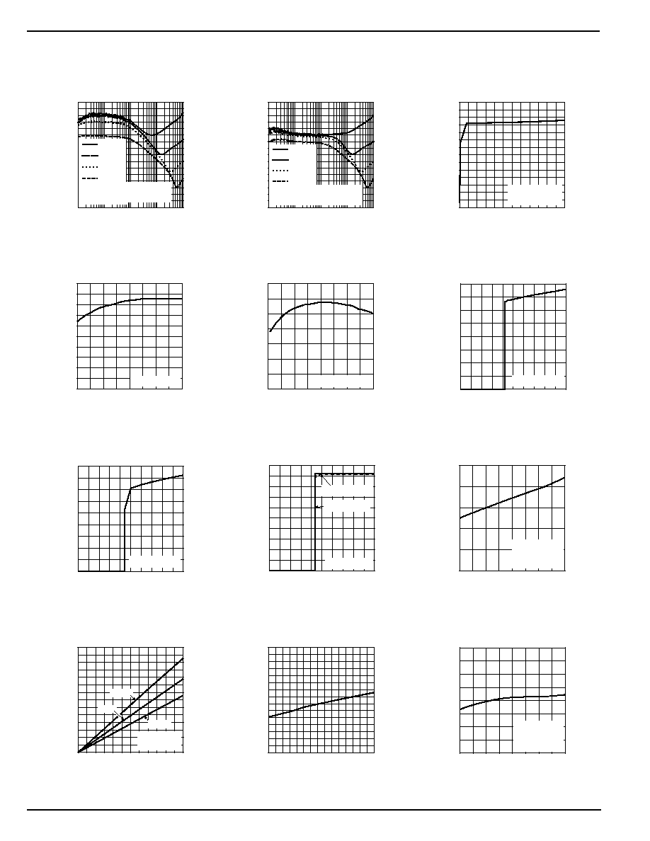
The MIC5253 is an efficient, CMOS voltage regulator opti-
mized for ultra-low-noise applications. It offers 1.5% initial
accuracy, extremely low dropout voltage (165mV at 100mA),
and low ground current (typically 95
µ
A at full load). The
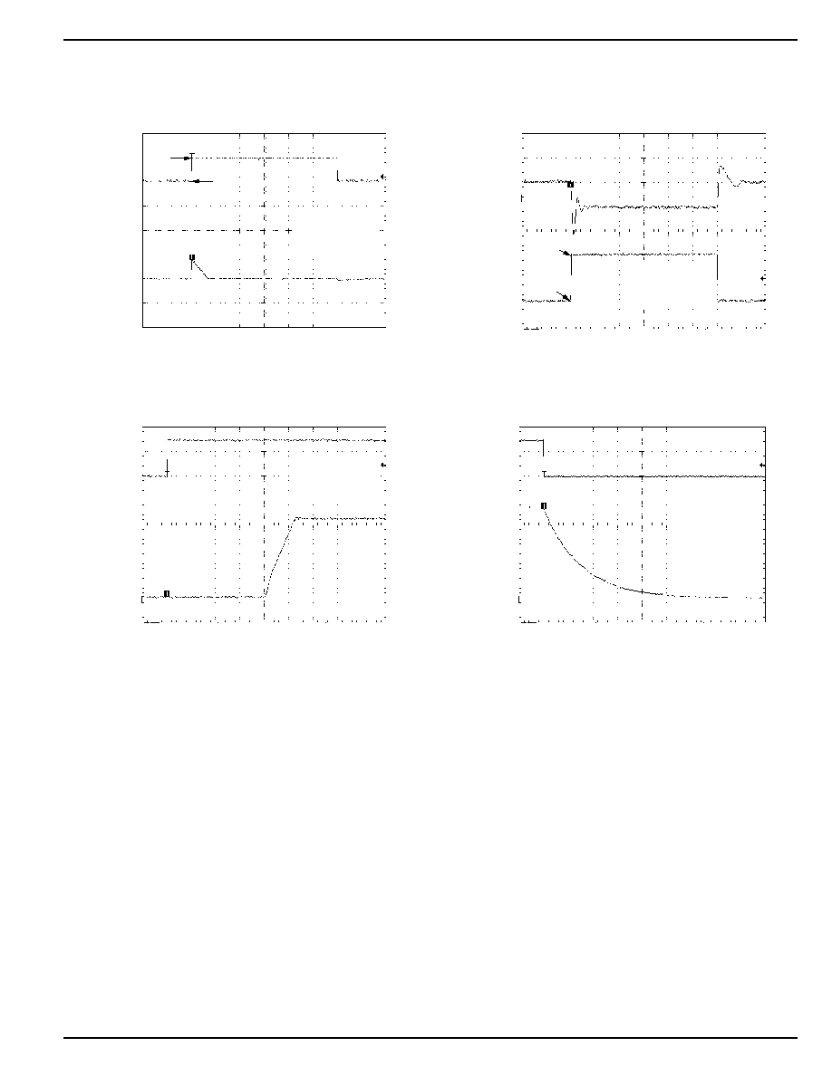
MIC5253 provides a very low noise output, ideal for RF
applications where a clean voltage source is required. A
noise bypass pin is also available for further reduction of
output noise.
Designed specifically for handheld and battery-powered de-
vices, the MIC5253 provides a TTL-logic-compatible enable
pin. When disabled, power consumption drops nearly to zero.
The MIC5253 also works with low-ESR ceramic capacitors,
reducing the amount of board space necessary for power
applications, critical in handheld wireless devices.
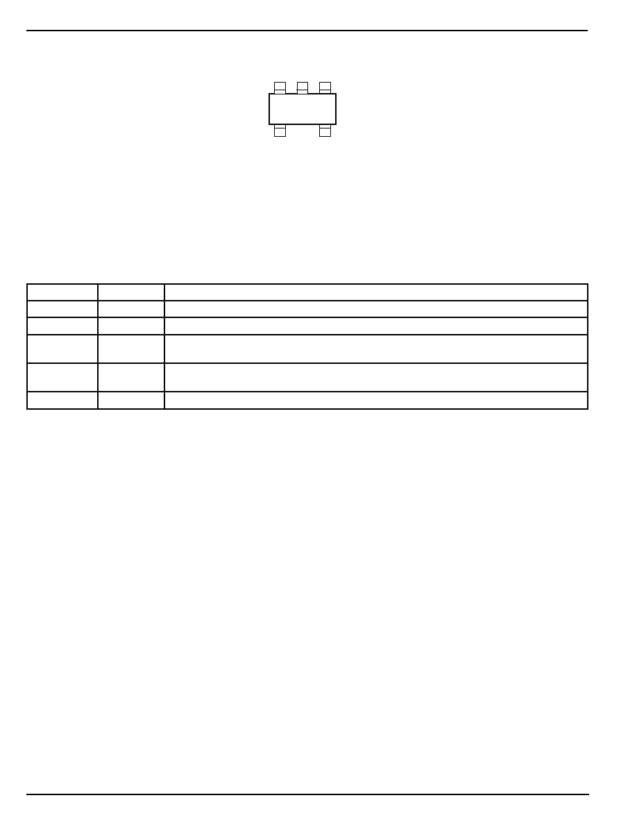
Available in the TeenyTM SC-70-5 package, the MIC5253
offers a wide range of output voltages. Key features include
current limit, thermal shutdown, faster transient response,
and an active clamp to speed up device turn-off.
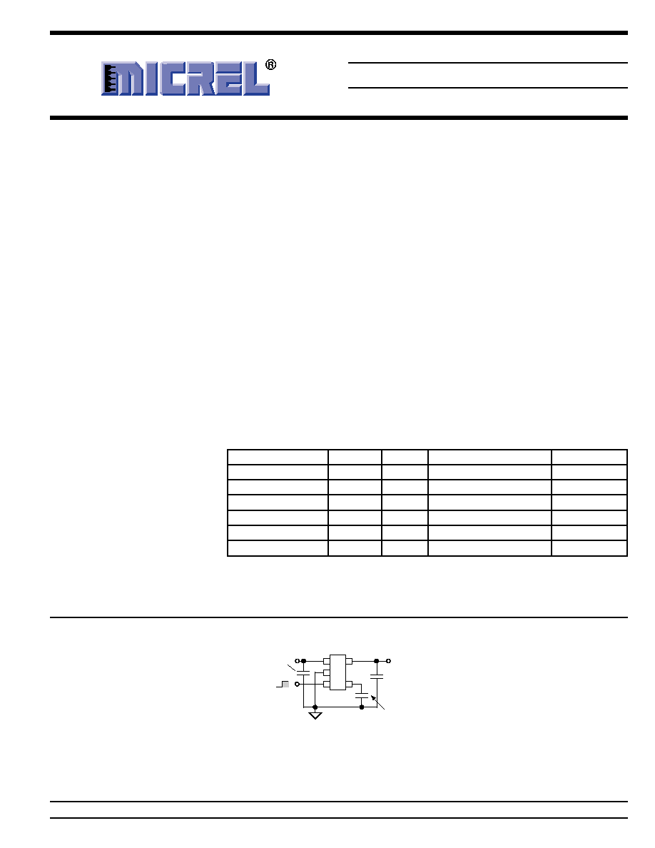
Typical Application
C
OUT
= 1.0
µ
F
C
IN
= 1.0
µ
F
Ceramic
Ceramic
1
5
2
3
4
C
BYP
= 0.01
µ
F
Enable
Shutdown
EN
V
OUT
MIC5253-x.xBC5
EN (pin 3) may be
connected directly
to IN (pin 1).
V
IN
Ultra-Low-Noise Regulator Application
Features
∑ Input voltage range: 2.7V to 5.5V
∑ TeenyTM SC-70-5 package
∑ Ultra-low output noise: 30
µ
V(rms)
∑ 100mA continuous output current, 150mA peak current
∑ Stability with ceramic output capacitors
∑ Ultralow dropout: 165mV @ 100mA
∑ High output accuracy:
1.5% initial accuracy
3.0% over temperature
∑ Low ground current: 95
µ
A
∑ TTL-Logic-controlled enable input
∑ "Zero" off-mode current
∑ Thermal shutdown and current limit protection
Applications
∑ Cellular phones and pagers
∑ Cellular accessories
∑ Battery-powered equipment
∑ Laptop, notebook, and palmtop computers
∑ Consumer/personal electronics
Micrel, Inc. ∑ 1849 Fortune Drive ∑ San Jose, CA 95131 ∑ USA ∑ tel + 1 (408) 944-0800 ∑ fax + 1 (408) 474-1000 ∑ http://www.micrel.com
Ordering Information
Part Number
Marking
Voltage
Junction Temp. Range*
Package
MIC5253-1.8BC5
LCN
1.8V
≠40
∞
C to +125
∞
C
SC-70-5
MIC5253-1.85BC5
L71J
1.85V
≠40
∞
C to +125
∞
C
SC-70-5
MIC5253-2.6BC5
LCP
2.6V
≠40
∞
C to +125
∞
C
SC-70-5
MIC5253-2.9BC5
L729
2.9V
≠40
∞
C to +125
∞
C
SC-70-5
MIC5253-3.0BC5
LCG
3.0V
≠40
∞
C to +125
∞
C
SC-70-5
MIC5253-3.3BC5
L733
3.3V
≠40
∞
C to +125
∞
C
SC-70-5
Other voltages available. Contact Micrel for details.
Teeny is a trademark of Micrel, Inc.
August 2004
3
M9999-081804
MIC5253
Micrel
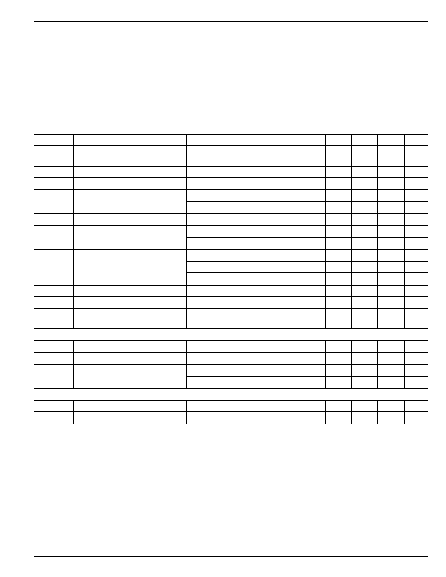
Electrical Characteristics
(5)
V
IN
= V
OUT
+ 1V, V
EN
= V
IN;
I
OUT
= 100
µ
A; T
J
= 25
∞
C, bold values indicate ≠40
∞
C
T
J
+125
∞
C; unless otherwise noted.
Symbol
Parameter
Conditions
Min
Typical
Max
Units
V
O
Output Voltage Accuracy
I
OUT
= 100
µ
A
≠1.5
1.5
%
≠3
3
%
V
LNR
Line Regulation
V
IN
= V
OUT
+ 1V to 6V
0.035
0.05
%/V
V
LDR
Load Regulation
I
OUT
= 0.1mA to 100mA, Note 6
1.5
2.5
%
V
IN
≠ V
OUT
Dropout Voltage
(7)
I
OUT
= 50mA
80
150
mV
I
OUT
= 100mA
165
300
mV
I
Q
Quiescent Current
V
EN
0.4V (shutdown)
0.2
1
µ
A
I
GND
Ground Pin Current
(8)
I
OUT
= 0mA
75
100
µ
A
I
OUT
= 100mA
90
150
µ
A
PSRR
Ripple Rejection
f = 100Hz, C
OUT
= 1.0
µ
F, C
BYP
= 0.1
µ
F
66
dB
f = 1kHz, V
IN
= V
OUT
+1, C
BYP
= 0.1
µ
F
70
dB
f = 10kHz, V
IN
= V
OUT
+1, C
BYP
= 0.1
µ
F
65
dB
t
ON
Turn-On Time
30
150
µ
s
I
LIM
Current Limit
V
OUT
= 0V
150
250
450
mA
e
n
Output Voltage Noise
C
OUT
= 1.0
µ
F, C
BYP
= 0.01
µ
F,
30
µ
V(rms)
f = 10Hz to 100kHz
Enable Input
V
IL
Enable Input Logic-Low Voltage
V
IN
= 2.7V to 5.5V, regulator shutdown
0.4
V
V
IH
Enable Input Logic-High Voltage
V
IN
= 2.7V to 5.5V, regulator enabled
1.6
V
I
EN
Enable Input Current
V
IL
0.4V, regulator shutdown
0.01
µ
A
V
IH
1.6V, regulator enabled
0.01
µ
A
Thermal Protection
Thermal Shutdown Temperature
150
∞
C
Thermal Shutdown Hysteresis
10
∞
C
Notes:
1.
Exceeding the absolute maximum ratings may damage the device.
2.
The device is not guaranteed to function outside its operating ratings.
3.
The maximum allowable power dissipation of any T
A
(ambient temperature) is P
D(max)
= (T
J(max)
≠T
A
)/
JA
. Exceeding the maximum allowable power
dissipation will result in excessive die temperature, and the regulator will go into thermal shutdown. The
JA
of the MIC5253-x.xBC5 (all versions) is
400
∞
C/W on a PC board (see "Thermal Considerations" section for further details).
4.
Devices are ESD sensitive. Handling precautions recommended.
5.
Specification for packaged product only.
6.
Regulation is measured at constant junction temperature using low duty cycle pulse testing. Parts are tested for load regulation in the load range from
0.1mA to 100mA. Changes in output voltage due to heating effects are covered by the thermal regulation specification.
7.
Dropout Voltage is defined as the input to output differential at which the output voltage drops 2% below its nominal value measured at 1V differential.
For outputs below 2.7V, dropout voltage is the input-to-output voltage differential with the minimum input voltage 2.7V. Minimum input operating voltage
is 2.7V.
8.
Ground pin current is the regulator quiescent current. The total current drawn from the supply is the sum of the load current plus the ground pin current.
Absolute Maximum Ratings
(1)
Supply Input Voltage (V
IN
) .................................. 0V to +7V
Enable Input Voltage (V
EN
) ................................. 0V to +7V
Power Dissipation (P
D
) ........................ Internally Limited
(3)
Junction Temperature (T
J
) ....................... ≠40
∞
C to +125
∞
C
Storage Temperature ............................... ≠65
∞
C to +150
∞
C
Lead Temperature (soldering, 5 sec.) ....................... 260
∞
C
ESD Rating
(4) ................................................................................
2kV
Operating Ratings
(2)
Input Voltage (V
IN
) ...................................... +2.7V to +5.5V
Enable Input Voltage (V
EN
) .................................. 0V to V
IN
Junction Temperature (T
J
) ....................... ≠40
∞
C to +125
∞
C
Thermal Resistance
SC-70-5
(
JA
) .................................................... 400
∞
C/W