
MIC5255
Micrel
June 2003
1
MIC5255
General Description
The MIC5255 is an efficient, precise CMOS voltage regulator
optimized for ultra-low-noise applications. It offers 1% initial
accuracy, extremely low dropout voltage (135mV at 150mA)
and low ground current (typically 90
µ
A). The MIC5255 pro-
vides a very low noise output, ideal for RF applications where
a clean voltage source is required. A noise bypass pin is also
available for further reduction of output noise.
Designed specifically for handheld and battery-powered de-
vices, the MIC5255 provides a TTL-logic-compatible enable
pin. When disabled, power consumption drops nearly to zero.
The MIC5255 also works with low-ESR ceramic capacitors,
reducing the amount of board space necessary for power
applications, critical in hand-held wireless devices.
Key features include current limit, thermal shutdown, faster
transient response, and an active clamp to speed up device
turn-off. Available in the IttyBittyTM SOT-23-5 package and
the new Thin SOT-23-5, which offers the same footprint as
the standard IttyBittyTM SOT-23-5, but only 1mm tall. The
MIC5255 offers a range of output voltages.
Typical Application
C
OUT
= 1.0
µ
F
C
IN
= 1.0
µ
F
Ceramic
Ceramic
1
5
2
3
4
C
BYP
= 0.01
µ
F
Enable
Shutdown
EN
V
OUT
MIC5255-x.xBM5
EN (pin 3) may be
connected directly
to IN (pin 1).
V
IN
Ultra-Low-Noise Regulator Application
MIC5255
150mA Low Noise
µ
Cap CMOS LDO
Final Information
Features
∑ Input voltage range: 2.7V to 6.0V
∑ Thin SOT package: 1mm height SOT-23-5
∑ Ultralow output noise: 30
µ
V(rms)
∑ Stability with ceramic output capacitors
∑ Ultralow dropout: 135mV @ 150mA
∑ High output accuracy:
1.0% initial accuracy
2.0% over temperature
∑ Low quiescent current: 90
µ
A
∑ Tight load and line regulation
∑ TTL-Logic-controlled enable input
∑ "Zero" off-mode current
∑ Thermal shutdown and current limit protection
Applications
∑ Cellular phones and pagers
∑ Cellular accessories
∑ Battery-powered equipment
∑ Laptop, notebook, and palmtop computers
∑ Consumer/personal electronics
Micrel, Inc. ∑ 1849 Fortune Drive ∑ San Jose, CA 95131 ∑ USA ∑ tel + 1 (408) 944-0800 ∑ fax + 1 (408) 944-0970 ∑ http://www.micrel.com
MIC5255
Micrel
MIC5255
2
June 2003
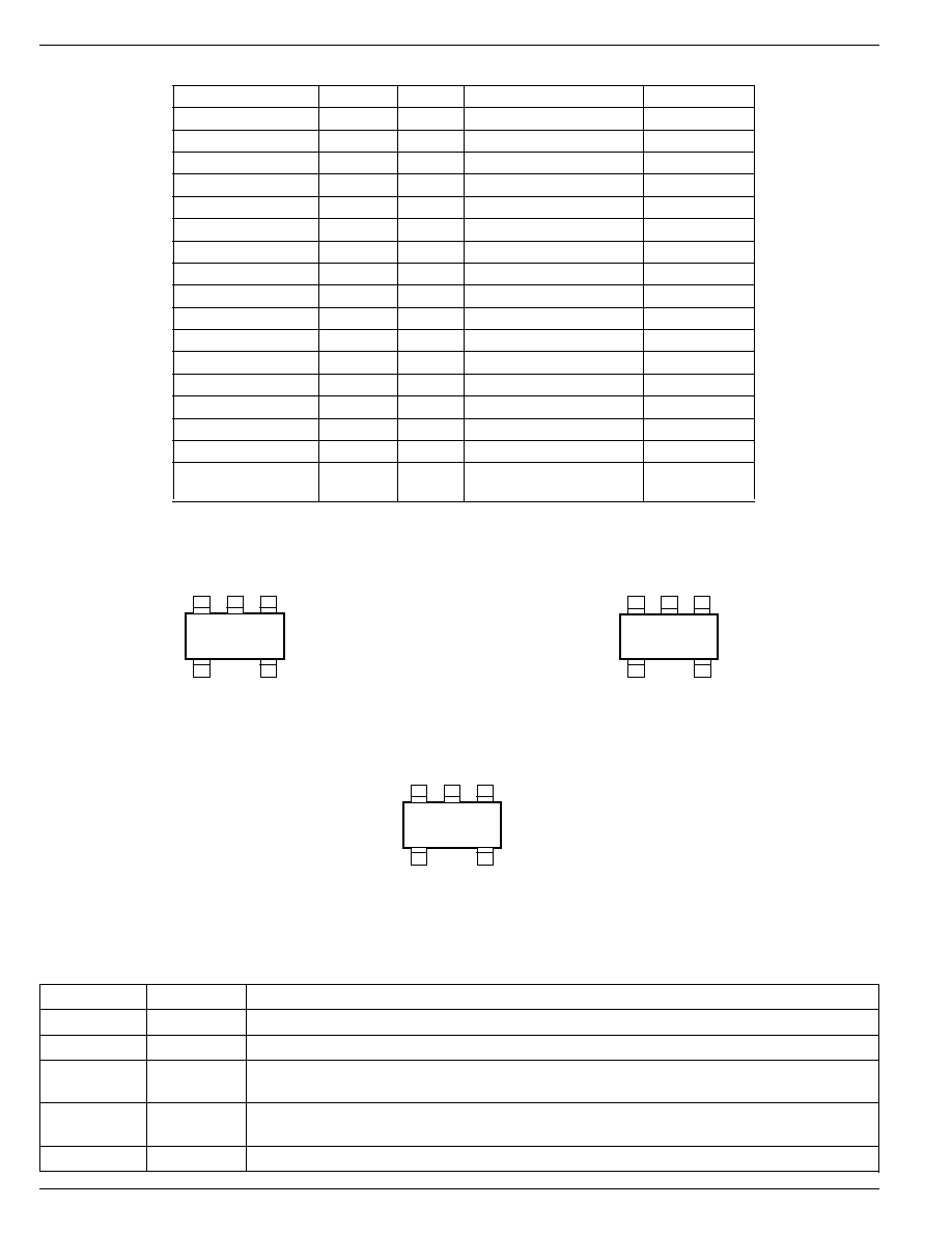
Pin Configuration
IN
OUT
BYP
EN
LWxx
1
3
4
5
2
GND
MIC5255-x.xBM5
(SOT-23-5)
Pin Description
Pin Number
Pin Name
Pin Function
1
IN
Supply Input.
2
GND
Ground.
3
EN
Enable/Shutdown (Input): CMOS compatible input. Logic high = enable; logic low = shutdown.
Do not leave open.
4
BYP
Reference Bypass: Connect external 0.01
µ
F
C
BYP
1.0
µ
F capacitor to GND to reduce output
noise. May be left open.
5
OUT
Regulator Output
Ordering Information
Part Number
Marking
Voltage
Junction Temp. Range
Package
MIC5255-2.5BM5
LW25
2.5V
≠40
∞
C to +125
∞
C
SOT-23-5
MIC5255-2.6BM5
LW26
2.6V
≠40
∞
C to +125
∞
C
SOT-23-5
MIC5255-2.7BM5
LW27
2.7V
≠40
∞
C to +125
∞
C
SOT-23-5
MIC5255-2.8BM5
LW28
2.8V
≠40
∞
C to +125
∞
C
SOT-23-5
MIC5255-2.85BM5
LW2J
2.85V
≠40
∞
C to +125
∞
C
SOT-23-5
MIC5255-2.9BM5
LW29
2.9V
≠40
∞
C to +125
∞
C
SOT-23-5
MIC5255-3.0BM5
LW30
3.0V
≠40
∞
C to +125
∞
C
SOT-23-5
MIC5255-3.1BM5
LW31
3.1V
≠40
∞
C to +125
∞
C
SOT-23-5
MIC5255-3.2BM5
LW32
3.2V
≠40
∞
C to +125
∞
C
SOT-23-5
MIC5255-3.3BM5
LW33
3.3V
≠40
∞
C to +125
∞
C
SOT-23-5
MIC5255-2.6BD5
NW26
2.6V
≠40
∞
C to +125
∞
C
TSOT-23-5
MIC5255-2.8BD5
NW28
2.8V
≠40
∞
C to +125
∞
C
TSOT-23-5
MIC5255-2.85BD5
NW2J
2.85V
≠40
∞
C to +125
∞
C
TSOT-23-5
MIC5255-2.9BD5
NW29
2.9V
≠40
∞
C to +125
∞
C
TSOT-23-5
MIC5255-3.0BD5
NW30
3.0V
≠40
∞
C to +125
∞
C
TSOT-23-5
MIC5255-3.3BD5
NW33
3.3V
≠40
∞
C to +125
∞
C
TSOT-23-5
MIC5255-2.5YM5
KW25
2.5V
≠40
∞
C to +125
∞
C,
TSOT-23-5
Lead free
Other voltages available. Contact Micrel for details.
IN
OUT
BYP
EN
NWxx
1
3
4
5
2
GND
MIC5255-x.xBD5
(TSOT-23-5)
IN
OUT
BYP
EN
KWxx
1
3
4
5
2
GND
MIC5255-x.xYM5
(SOT-23-5)

MIC5255
Micrel
June 2003
3
MIC5255
Electrical Characteristics
V
IN
= V
OUT
+ 1V, V
EN
= V
IN;
I
OUT
= 100
µ
A; T
J
= 25
∞
C, bold values indicate ≠40
∞
C
T
J
+125
∞
C; unless noted.
Symbol
Parameter
Conditions
Min
Typical
Max
Units
V
O
Output Voltage Accuracy
I
OUT
= 100
µ
A
≠1
1
%
≠2
2
%
V
LNR
Line Regulation
V
IN
= V
OUT
+ 1V to 6V
0.02
0.05
%/V
V
LDR
Load Regulation
I
OUT
= 0.1mA to 150mA, Note 5
1.5
2.5
%
V
IN
≠ V
OUT
Dropout Voltage, Note 6
I
OUT
= 100
µ
A
0.1
5
mV
I
OUT
= 100mA
90
150
mV
I
OUT
= 150mA
135
200
mV
250
mV
I
Q
Quiescent Current
V
EN
0.4V (shutdown)
0.2
1
µ
A
I
GND
Ground Pin Current, Note 7
I
OUT
= 0mA
90
150
µ
A
I
OUT
= 150mA
117
µ
A
PSRR
Ripple Rejection
f = 10Hz, C
OUT
= 1.0
µ
F, C
BYP
= 0.01
µ
F
60
dB
f = 100Hz, V
IN
= V
OUT
+1
60
dB
f = 10kHz, V
IN
= V
OUT
+1
50
dB
I
LIM
Current Limit
V
OUT
= 0V
160
425
mA
e
n
Output Voltage Noise
C
OUT
= 1.0
µ
F, C
BYP
= 0.01
µ
F,
30
µ
V(rms)
f = 10Hz to 100kHz
Enable Input
V
IL
Enable Input Logic-Low Voltage
V
IN
= 2.7V to 5.5V, regulator shutdown
0.4
V
V
IH
Enable Input Logic-High Voltage
V
IN
= 2.7V to 5.5V, regulator enabled
1.6
V
I
EN
Enable Input Current
V
IL
0.4V, regulator shutdown
0.01
µ
A
V
IH
1.6V, regulator enabled
0.01
µ
A
Shutdown Resistance Discharge
500
Thermal Protection
Thermal Shutdown Temperature
150
∞
C
Thermal Shutdown Hysteresis
10
∞
C
Note 1.
Exceeding the absolute maximum rating may damage the device.
Note 2.
The device is not guaranteed to function outside its operating rating.
Note 3.
The maximum allowable power dissipation of any T
A
(ambient temperature) is P
D(max)
= T
J(max)
≠T
A
/
JA
. Exceeding the maximum allowable
power dissipation will result in excessive die temperature, and the regulator will go into thermal shutdown. The
JA
of the MIC5255-x.xBM5 (all
versions) is 235
∞
C/W on a PC board (see "Thermal Considerations" section for further details).
Note 4.
Devices are ESD sensitive. Handling precautions recommended.
Note 5.
Regulation is measured at constant junction temperature using low duty cycle pulse testing. Parts are tested for load regulation in the load
range from 0.1mA to 150mA. Changes in output voltage due to heating effects are covered by the thermal regulation specification.
Note 6.
Dropout Voltage is defined as the input to output differential at which the output voltage drops 2% below its nominal value measured at 1V
differential. For outputs below 2.7V, dropout voltage is the input-to-output voltage differential with the minimum input voltage 2.7V. Minimum
input operating voltage is 2.7V.
Note 7.
Ground pin current is the regulator quiescent current. The total current drawn from the supply is the sum of the load current plus the ground
pin current.
Absolute Maximum Ratings
(Note 1)
Supply Input Voltage (V
IN
) .................................. 0V to +7V
Enable Input Voltage (V
EN
) ................................. 0V to +7V
Power Dissipation (P
D
) ............... Internally Limited, Note 3
Junction Temperature (T
J
) ....................... ≠40
∞
C to +125
∞
C
Storage Temperature ............................... ≠65
∞
C to +150
∞
C
Lead Temperature (soldering, 5 sec.) ....................... 260
∞
C
ESD, Note 4 .................................................................. 2kV
Operating Ratings
(Note 2)
Input Voltage (V
IN
) ......................................... +2.7V to +6V
Enable Input Voltage (V
EN
) .................................. 0V to V
IN
Junction Temperature (T
J
) ....................... ≠40
∞
C to +125
∞
C
Thermal Resistance
SOT-23
(
JA
) ..................................................... 235
∞
C/W

MIC5255
Micrel
MIC5255
4
June 2003
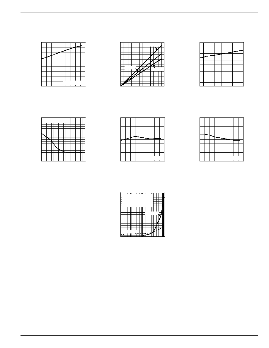
Typical Characteristics
0
10
20
30
40
50
60
70
10
100
1000
10000
100000
1000000
PSRR (dB)
FRQUENCY (Hz)
100
µ
A*
50mA*
100mA*
150mA*
Power Supply Rejection Ratio
*I
LOAD
C
OUT
= 1
µ
F Ceramic
0
10
20
30
40
50
60
70
10
100
1000
10000
100000
1000000
PSRR (dB)
FRQUENCY (Hz)
100
µ
A*
50mA*
100mA*
150mA*
Power Supply Rejection Ratio
* I
LOAD
C
OUT
= 4.7
µ
F Ceramic
0
10
20
30
40
50
60
70
10
100
1000
10000
100000
1000000
PSRR (dB)
FRQUENCY (Hz)
0
µ
F*
0.01
µ
F*
0.1
µ
F*
1.0
µ
F*
Power Supply Rejection Ratio
* C
BYP
I
LOAD
= 50mA
V
IN
= V
OUT
+ 0.5V
C
OUT
= 1
µ
F Ceramic
0
10
20
30
40
50
60
70
80
0
200
400
600
800
1000
PSRR (dB)
VOLTAGE DROP (mV)
PSRR vs. Voltage Drop
I
LOAD
= 100
µ
A
I
LOAD
= 150mA
C
OUT
= 1
µ
F
C
BYP
= 0.01
µ
F
100
105
110
115
120
125
130
0.1
1
10
100
1000
GROUND CURRENT (
µ
A)
OUTPUT CURRENT (mA)
Ground Pin Current
V
IN
= V
OUT
+ 1V
95
97
99
101
103
105
107
109
111
113
115
-40 -20 0 20 40 60 80 100120140
GROUND CURRENT (
µ
A)
TEMPERATURE (
∞
C)
Ground Pin Current
I
LOAD
= 100
µ
A
95
100
105
110
115
120
125
-40 -20 0 20 40 60 80 100120140
GROUND CURRENT (
µ
A)
TEMPERATURE (
∞
C)
Ground Pin Current
I
LOAD
= 150mA
0
20
40
60
80
100
120
140
0 0.5 1 1.5 2 2.5 3 3.5 4 4.5 5
GROUND CURRENT (
µ
A)
INPUT VOLTAGE (V)
Ground Pin Current
I
LOAD
= 100
µ
A
0
20
40
60
80
100
120
140
0 0.5 1 1.5 2 2.5 3 3.5 4 4.5 5
GROUND CURRENT (
µ
A)
INPUT VOLTAGE (V)
Ground Pin Current
I
LOAD
= 150mA
0
0.5
1
1.5
2
2.5
3
3.5
0 0.5 1 1.5 2 2.5 3 3.5 4 4.5 5
OUTPUT VOLTAGE (V)
INPUT VOLTAGE (V)
Dropout Characteristics
I
LOAD
= 150mA
I
LOAD
= 100
µ
A
0
0.02
0.04
0.06
0.08
0.1
0.12
0.14
-40 -20 0 20 40 60 80 100120140
DROPOUT VOLTAGE (mV)
TEMPERATURE (
∞
C)
Dropout Voltage
I
LOAD
= 100
µ
A
0
10
20
30
40
50
60
70
0
200
400
600
800
1000
PSRR (dB)
VOLTAGE DROP (mV)
PSRR vs. Voltage Drop
I
LOAD
= 100
µ
A
I
LOAD
= 150mA
C
OUT
= 1
µ
F
C
BYP
= 0
MIC5255
Micrel
June 2003
5
MIC5255
0
20
40
60
80
100
120
140
160
180
0
20 40 60 80 100 120 140 160
DROPOUT VOLTAGE (mV)
OUTPUT CURRENT (mA)
Dropout Voltage
T = ≠40C
T = 25C
T = 125C
0
100
200
300
400
500
600
3
3.5
4
4.5
5
5.5
6
SHORT CIRCUIT CURRENT (mA)
INPUT VOLTAGE (V)
Short Circuit Current
400
410
420
430
440
450
460
470
480
490
500
-40 -20 0 20 40 60 80 100120140
SHORT CIRCUIT CURRENT (mA)
TEMPERATURE (
∞
C)
Short Circuit Current
V
IN
= V
OUT
+ 1V
2.95
2.96
2.97
2.98
2.99
3.00
3.01
3.02
3.03
3.04
3.05
-40 -20 0 20 40 60 80 100120140
OUTPUT VOLTAGE (V)
TEMPERATURE (
∞
C)
Output Voltage vs.
Temperature
I
LOAD
= 100
µ
A
0.8
0.85
0.9
0.95
1
1.05
1.1
1.15
1.2
1.25
1.3
-40 -20 0 20 40 60 80 100120140
ENABLE THRESHOLD VOLTAGE (V)
TEMPERATURE (
∞
C)
Enable Threshold
vs. Temperature
I
LOAD
= 100
µ
A
0
50
100
150
200
250
300
350
400
450
500
100
1000
10000 100000 1000000
TIME (
µ
s)
BYPASS CAPACITANCE (pF)
Turn-On Time vs.
Bypass Capacitance
Prop Delay
Rise Time
C
IN
= 1
µ
F Ceramic
C
OUT
= 1
µ
F Ceramic
I
LOAD
= 100
µ
A
0
20
40
60
80
100
120
140
160
180
-40 -20 0 20 40 60 80 100120140
DROPOUT VOLTAGE (mV)
TEMPERATURE (
∞
C)
Dropout Voltage
I
LOAD
= 150mA